

SGS Thomson Microelectronics GS-R415-2, GS-R412-2, GS-R405-2, GS-R424-2, GS-R400V-2 Datasheet
SWITCHING REGULATOR FAMILY
FEATURES
MTBF in excess of 500,000 hours
4A max output current
40V max input voltage
4V max dro p-o ut vo ltage
Soft start
Non-latching short circuit protection
Crow-bar outpu t over volta ge prote ct ion
DESCRIPTION
The GS-R400/2 series is a family of small sized
high current, high voltage step-down switching
regulators.
The integral heatsink allows a large power handling
capability and it provides also an effective shielding
to minimize EMI.
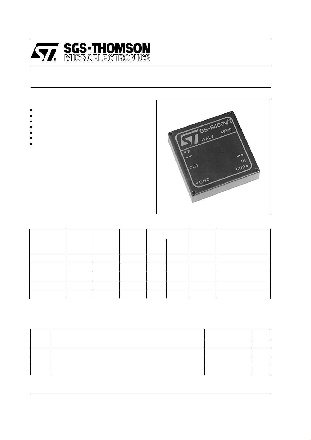
GS-R400/2 Family
SMALL SIZE STEP-DOWN
SELECTION CHART
Type
Ordering
Number
GS-R405/2
GS-R412/2
GS-R415/2
GS-R424/2
GS-R400V/2
Note : Line regulation is measured at I
Load regulation is measured at Vin=Vo+8V and I
Case temperature must be kept below 85° C
Output
Voltage
(V)
5.1 ± 2%
12.0 ± 4%
15.0 ± 4%
24.0 ± 4%
5.1 to 24
9 to 40
16 to 40
19 to 40
28 to 40
V o+4 to 40
Input
Voltage
(V)
=1A.
out
Output
Ripple
(mVpp)
25 2 20 80
50 5 40 85 "
65 6 60 87 "
100 6 80 90 "
25 to 100 2 to 6 20 to 80 80 to 90
=0.5 to 1.5A.
out
Regulation
Line
(mV/V)
Load
(mV/A)
Efficiency
Notes
(%)
Fixed output voltage
Progr. output voltage
ABSOLUTE MAXIMUM RATINGS
Symbol Parameter Value Unit
DC Input Voltage
V
i
Output Current
I
o
T
T
cop
Storage Temperature Range
stg
Operating Case Temperature Range
42 V
4A
– 40 to +105 °C
– 20 to +85 °C
June 1994 1/3

GS- R4 0 0/2 F A M I LY
CONNECTION DIAGRAM AND MECHANICAL DATA
Dimensions in mm Bottom view
Pin 5 GS-R400V/2 only
PIN DESCRIPTION
Pin Function Description
+ Input DC input voltage. Recommended maximum voltage is 40V.
1
Input GND Return for input voltage source.
2
Output GND Return for output c urrent path. Internally connected to pin 2.
3
+ Output Regulated DC output voltage.
4
Program A resistor (<10kΩ) connected between this pin and pin 4 sets the + output voltage of the
5
GS-R400V/2.
ELECTRICAL CHARACTERISTICS (TA = 25°C unless otherwise specified)
Symbol Parameter Test Conditions Min Typ Max Unit
∆Vo/∆T
I
I
S
t
t
V
R
Temperature Stability Vi = Vo+8V Io = 1A
Output Current Vi = Vo+8V
I
o
Current Limit Vi = Vo+8V
oL
Average Input Current Vi = 40V Output Shorted
isc
Switching Frequency Io = 1A
f
s
Supply Voltage Rejection fo = 100Hz Io = 1A
VR
Ripple Voltage Io = 1A
V
r
Soft Start Time
ss
Crowbar Delay Time
cb
Crowbar Intervention Threshold
cth
Thermal Resistance Case to ambient
th
0.2/0.6 mV/°C
0.1 4 A
58A
0.1 0.2 A
100 kHz
4/12 mV/V
25/100 mVpp
10/35 ms
5 µs
Vo•1.25 V
8 °C/W
2/3
 Loading...