


GS-R1012
120W STEP-DOWN SWITCHING REGULATOR
Type V
GS-R1012 18 to 36 V 12 V 10 A
i
V
o
I
o
FEATURES
Wide inputvoltage range (18 to 36V)
High efficiency(90%min.)
Paralleloperation with current sharing
Synchronization
Remote inhibit/enable
Remote load voltage sense
Output short-circuitprotection
Soft-start
PCB or chassismountable
DESCRIPTION
The GS-R1012 is a step-down switching voltage
regulator suitable to provide 12V/10A output voltage from a wide input voltage range (18 to 36V).
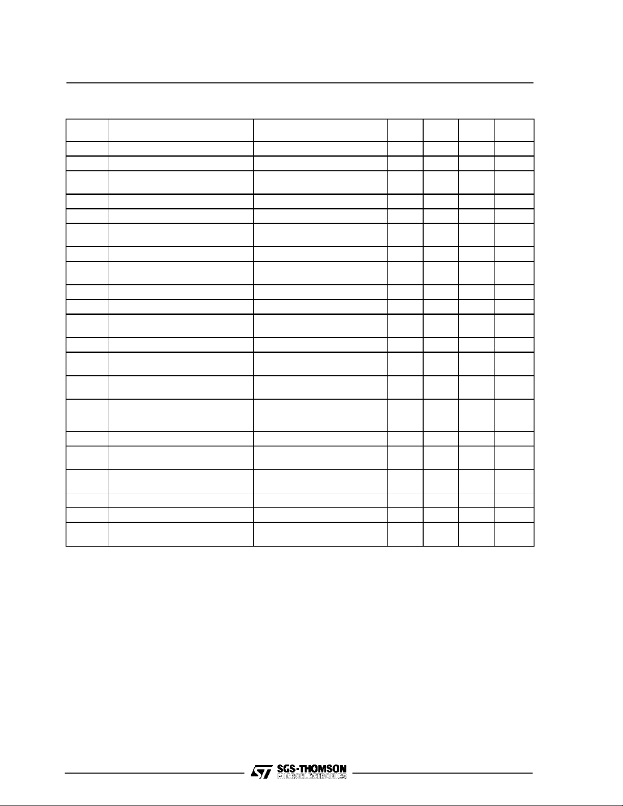
ABSOLUTE MAXIMUM RATINGS
Symbol Parameter Value Unit
DC Input Voltage
High Inhibit voltage
Storage Temperature Range
Operating Case Temperature Range
40 V
28 V
– 20 to +105 °C
0 to +75 °C
V
T
T
V
iinh
stg
cop
i
June 1994 1/7
GS-R1012
ELECTRICALCHARACTERISTICS (T
Symbol
Input Voltage Vo= 12V Io= 1.5 to 10A
V
i
Input Current Vi= 24V Io= 10A
l
i
Reflected Input Current Vi= 24V Io= 10A
l
ir
V
V
l
iinh
V
V
δV
δV
∆V
I
I
osc
δI
t
tr1
tr2
R
* Note: when output current isless than1.5A, output ripple voltage increases due to discontinuous operation.
Enable Input Voltage Vi= 18 to 36V Io= 1.5 to 10A
ien
Inhibit Input Voltage Vi= 18 to 36V Io= 1.5 to 10A
iinh
Inhibit Input Current Vi= 18 to 36V Io=1.5 to 10A
Output Voltage Vi= 18 to 36V Io= 1.5 to 10A
o
Output Ripple
or
Voltage
Line Regulation Vi= 18 to 36V Io= 10A
OL
Load Regulation Vi= 24V Io= 1.5 to 10A
OO
Remote Sense
o
Compensation
Output Current* Vi= 18 to 36V Vo= 12V
I
o
Output Current
ol
Limiting
Short-circuit Output
Current
Current Sharing
o
Deviation
Soft-start Time Vi= 24V Io= 10A
ss
Line Transient
Recovery Time
Load Transient
Recovery Time
Switching Frequency Vi= 24V Io= 1.5 to 10A
f
s
η Efficiency Vi
Thermal Resistance
thc
Case-to-ambient
Parameter Test Conditions Min Typ Max Unit
=25°C unless otherwise specified)
amb
with external filter (C = 1000µF)
V
=5V
iinh
Vi= 24V
Io= 10A
Vi= 24V
Io= 10A
Vi= 18 to 36V
Vi= 24V
Vi= 24V
Io= 2 to 10A two modules in
parallel
Vi= 15 to 36V
Io=5A
Vi= 24V Io= 1.5 to 10A
= 18 to 36V Io= 10A
18 24 36 V
0 1.2 V
224V
11.4 12 12.6 V
010A
10.5 11.5 A
90 92 %
5,6 A
400 500 mApp
0.3 0.5 mA
150 mVpp
0.5 %
1%
0.5 V
16 A
10 %
15 ms
60 µs
100 µs
100 kHz
7.5 °C/W
2/7
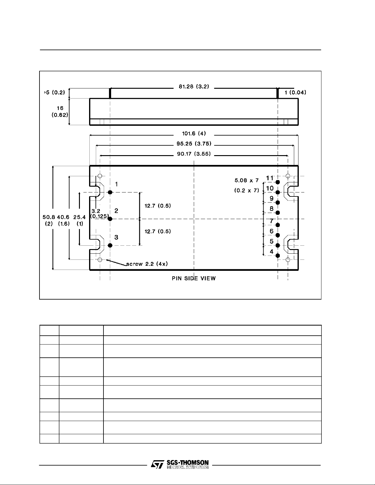
CONNECTION DIAGRAM AND MECHANICAL DATA
GS-R1012
Dimensionsin mm (inches).
PIN DESCRIPTION
Pin Function Description
1 GND Input
2 Inhibit
3 + Vin
4,5 + Vout
6 + Sense
7 Sync
8 Parallel
9 -Sense
10,11 GND Output
Return for input voltage source. Internally connected topin 10,11.
The converter is ON (Enable) when this pin is unconnected or the voltageapplied is lower
than 1.2V.The converter is OFF (Inhibit) for a control voltage in the range of 2 to24V.
DC Input voltage; recommended maximum voltage is 36V.
External capacitor between pin 3and pin 1 is mandatory; recommended value is
1000µF/50V for switching application.
+12V output voltage.
Senses the remote load high side. To be connectedto pin4,5 when remote sense is not
used.
Synchronization output. See figures 1,2,3,4. Take care to leave the pin open when is not
used.
Parallel output. See figures 1,2,3,4. Takecare to leave the pin open when is not used.
Senses the remote load return. To be connected to pin 10,11 when remote sense is not
used.In parallel configuration, take care to connect all -S pins together (see figures 1,2,3,4).
Return for output current path. Internally connected to pin 1.
3/7

GS-R1012
USER NOTES
Input Voltage
The recommended operating maximum DC input
voltage is 36V inclusive of the ripplevoltage. The
use of an external low ESR, high ripple current
capacitor located as close the module as possible
is mandatory;recommendedvalue is 1000µF/50V.
Softstart
To avoid heavy inrush current the output voltage
rise time is typically15ms in anyconditionof load.
Remote Sensing
The remote voltage sense compensationrange is
for a totaldrop of 500mV equally shared between
the load connectingwires. It is a good practice to
shield the sensing wires to avoidoscillations. See
the connection diagramon figures 1, 2, 3, 4.
Figure1. Figure 2.
ParallelOperation
To increase available output regulated power, the
module features the parallelconnectionpossibility
with equal currentsharingand maximum deviation
of 10% (two modulesin parallel). See the connection diagram on figures 1, 2, 3, 4.
Module Protection
The module is protected against occasional and
permanent shortcircuits of the output pins to
ground,as well as against output current overload.
It usesa currentlimitingprotectioncircuitry, avoiding latch-up problems with certain types of loads.
4/7

Figure 3. Figure 4.
GS-R1012
Thermal characteristics: how to choose the
heat-sink
Sometimes the GS-R1012 requires an external
heat-sink depending both operating temperature
conditionsand power.
Beforeentering into calculationsdetails, some basic concepts will be explainedto better understand
the problem.
The thermal resistance between two points is representedby theirtemperature differencein front of
a specifieddissipatedpower, and it is expressedin
Degree Centigrade per Watt (°C/W).
For GS-R1012 thethermal resistancecase to ambientis7.5°C/W. This means that an internalpower
dissipationof 1Wwill bring thecasetemperatureat
7.5°C abovethe ambient temperature.
The maximumcasetemperaturetowhich themod-
ule provides 10Ais 75°C (see fig. 6).
Let’ssuppose to have a GS-R1012that delivers a
load current of 10Aat an ambient temperature of
40°C.
Thedissipated powerin thisoperating condition is
about10.4W (at typicalefficiencyof 92%), and the
casetemperatureof the modulewill be:
T
= T
Case
Amb
+ Pd× R
=40 + 10.4 × 7.5 = 118°C
th
Thisvalueexceedsthemaximumallowedtemperature and an external heat-sink must be added. To
this purpose four holes (see mechanical drawing)
areprovided on themetal surface of the module.
To calculatethisheat-sink,let’sfirstdeterminewhat
the totalthermal resistanceshould be.
T
CaseMAX
=
R
th
− T
P
d
amb
75
− 40
=
= 3.37°C/W
10.4
This value is the resulting value of the additional
heatsinkthermal resistance.
5/7

GS-R1012
Figure5. - Efficiency vs. Output Current.
Typ. eff. (%)
98
97
96
95
94
93
92
91
90
89
88
012345678910
Vi= 18V
Vi= 24V
Vi= 36V
Figure6. - Output Currentvs. T case.
6/7

GS-R1012
The following list may help the designer to select
the propercommerciallyavailableheat-sink.
Sometimes it can be more convenient to use a
Manufacturers Type Height (mm) Rth (°C/W)
ALUTRONIC PR139 20 3
PR140 19 2
PR159 20 2.5
ASSMAN V5440 19 3
V5805 15 2
V5280 19 2
AAVID 60885 14 4.5
60660 25.5 1.5
62355 33.5 3
AUSTERLITZ KS50 12 3
KS100.3 15 2.5
FISCHER SK16 25.5 1.5
SK52 19 2
SGE BOSARI L30 21 3
LZ50 24 3
THERMALLOY 6155 14 4.5
6601 14 5
6176 24 4.5
6320 30 1.5
custom made heat-sink that can be experimently
designed and tested.
Information furnished is believed to be accurate and reliable. However, SGS-THOMSON Microelectronics assumes no responsibility for the
consequences of use of such informationnor for any infringement of patents or other rights of third parties which may result from its use. No
license is granted by implicationor otherwise under any patent or patent rights of SGS-THOMSON Microelectronics. Specification mentioned
in this publication are subject to change without notice. This publication supersedes and replaces all information previously supplied.
SGS-THOMSON Microelectronics productsare notauthorized for use ascritical components inlife supportdevices or systems without express
written approval of SGS-THOMSON Microelectronics.
1994 SGS-THOMSON Microelectronics – All Rights Reserved
Australia - Brazil - China - France - Germany -Hong Kong - Italy - Japan - Korea - Malaysia - Malta - Morocco - The Netherlands -
Singapore - Spain - Sweden - Switzerland - Taiwan- Thailand - United Kingdom -U.S.A.
SGS-THOMSON Microelectronics GROUP OF COMPANIES
7/7
 Loading...