

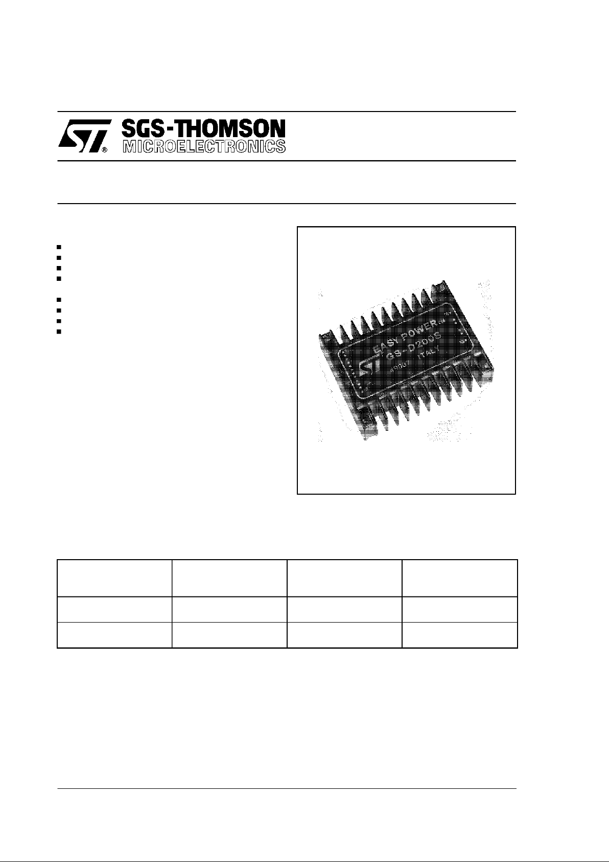
GS-D200
GS-D200S
2/2.5A BIPOLAR STEPPER MOTOR DRIVE MODULES
June 1994 1/17
FEATURES
Wide supply voltage range
Full/Half step drive capability
Logic signals TTL/CMOS compatible
Programmable motorphasecurrent andchopper
frequency
Selectable Slow/Fast current decay
Synchronization for multimotor applications
Remote shut-down
Home position indication
DESCRIPTION
The GS-D200 and the GS-D200S are drive modulesthat directlyinterface amicroprocessorto atwo
phase,bipolar, permanent magnet stepper motors.
The phase current is chopper controlled, and the
internal phase sequence generation reduces the
burden of the controller and it simplifies software
development.
TheGS-D200 uses bipolar power outputs whilethe
GS-D200S has powermos outputs to significantly
reduce both commutation and conduction losses.
A further benefit offered by the GS-D200S is the
completeprotection ofthe outputs againstany type
of shorts.
SELECTION CHART
Type
Ordering
Number
Phase
Current
(A)
Voltage
Drop
(V)
Supply
Voltage
(V)
GS-D200
1.0 nom.
(0.5 to 2.0)
4.1 max.
10 to 46
5.0±5%
GS-D200S
2.0 nom.
(0.5 to 2.5)
2.5 max.
12 to 40
5.0±5%
2/17
ABSOLUTEMAXIMUM RATINGS
Symbol Parameter Value Unit
V
s
DC Supply Voltage (pin 18)
GS-D200
GS-D200S
48
42
V
V
V
ss
DC Logic Supply Voltage(pin 12)
7V
T
stg
Storage TemperatureRange
– 40 to +105 °C
T
cop
Operating Case Temperature Range
– 20 to +85 °C
ELECTRICAL CHARACTERISTICS (TA=25°C and VS=24V unless otherwise specified)
Symbol Parameter Test Conditions
Value
Unit
Min Typ Max
I
s
Quiescent Supply Current Pin 18
20 mA
I
ss
Quiescent Logic Supply Current Pin 12 Vss=5V
60 mA
V
i
Input Voltage
Pin
3,4,6,7,10,1 1
Low
High
2
0.8
V
ss
V
V
I
i
Input Current
Pin
3,4,6,7,10,1 1
Vi=Low
Vi=High
0.6
10
mA
µA
V
sat
Source/Sink Saturation Voltage(GS-D200)
Pin
14,15,16,17
Io=1A
1.8 V
V
sat
Source/Sink SaturationVoltage(GS-D200S)
Pin
14,15,16,17
Io=2A
1.8 V
I
oL
Current Limit Intervention GS-D200S
5A
f
c
Chopper Frequency
17 kHz
t
clk
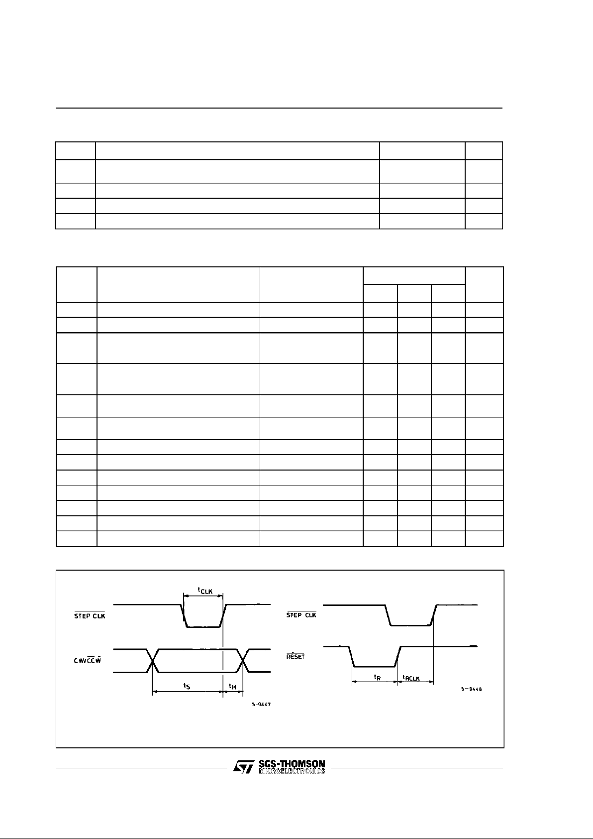
Stepckl Width Pin6 (Seefig. 1)
0.5 µs
t
s
Set Up Time
”1 µs
t
h
Hold Time
”1 µs
t
r
Reset Width
”1 µs
t
rclk
Reset to Clock Set Up Time
”1 µs
Figure 1: Signals Timing
GS-D200/GS-D200S
3/17
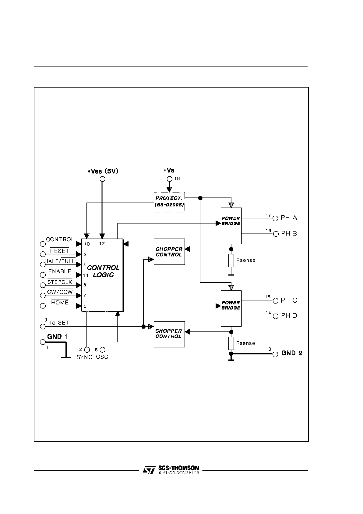
Figure2: GS-D200 and GS-D200SBlock Diagram
GS-D200/GS-D200S
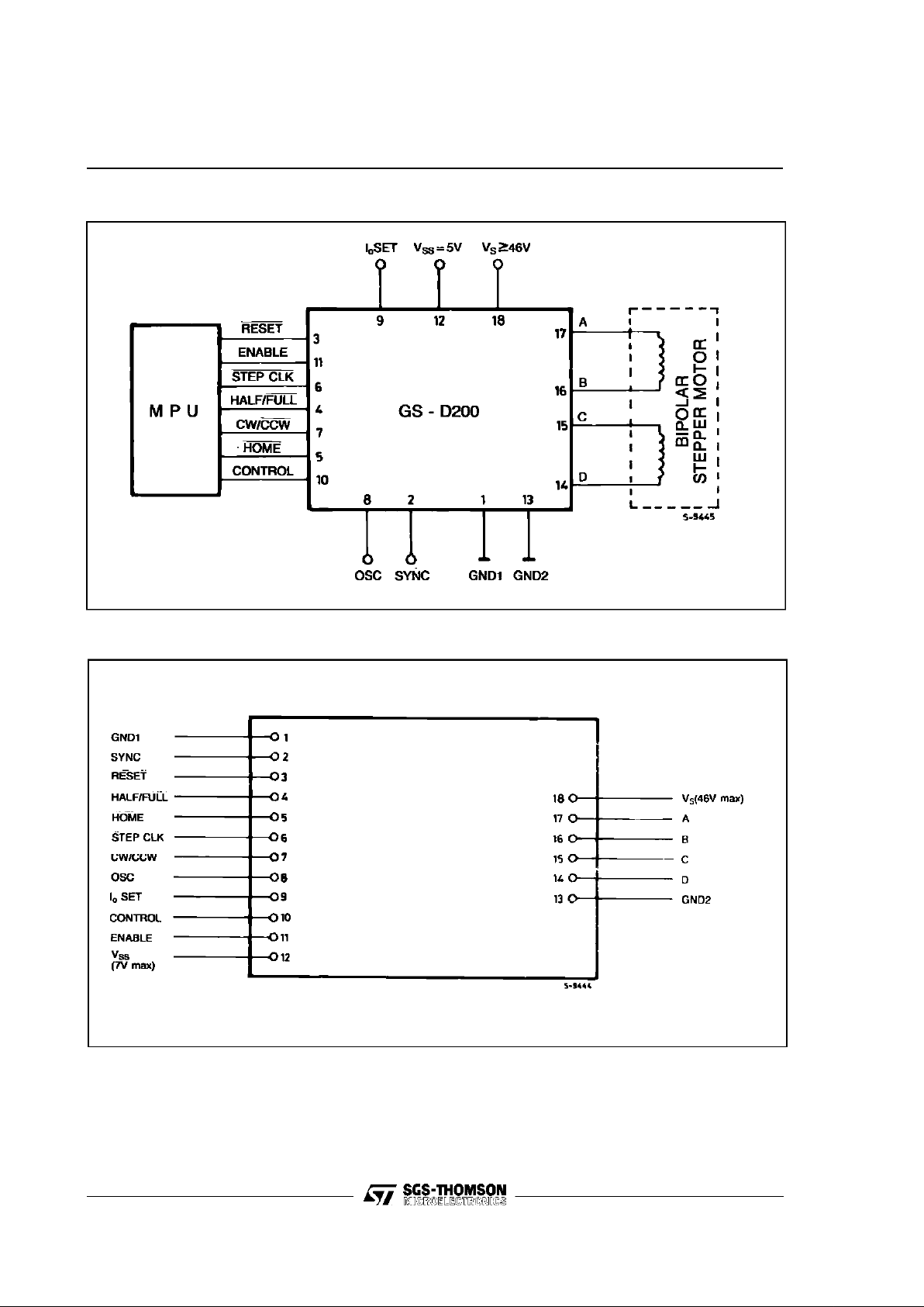
Figure 3: GS-D Modules Typical Application
4/17
Figure 4: GS-D200 and GS-D200S Connection Diagram (Topview)
GS-D200/GS-D200S
5/17
PIN DESCRIPTION
Pin Function Description
1
GND1 Return path for thelogic signals and 5V supply.
2
Sync
Chopper oscillatoroutput.
Several modules can be synchronized by connecting together all Sync pins. This pin can
be used as the input for an external clock source.
3
Reset
Asynchronousreset input. An active low pulse on this input preset the internal logicto the
initial state (ABCD=0101).
4
Half/Full
Half/Full step selection input.
When high or unconnectedthe halfstep operation is selected.
5
Home
When high, this output indicates that the internal counteris in its initial state (ABCD=0101).
This signal may be usedin conjunctionwith a mechanical switch to ground or with open
collectoroutput of an optical detector to be used as a systemhome detector.
6
Stepclk The motor is movedone stepon therisingedge of this signal.
7
CW/CCW
Direction controlinput. When high orunconnected clockwiserotation is selected. Physical
direction of motor rotationdepends also on windings connection.
8
Oscillator
The chopper oscillatortiming, internally fixed at 17kHz, can be modified by connecting a
resistor between this pin and Vssor a capacitor between this pin and Gnd1.
The oscillatorinput mustbe groundedwhen the unit is externally synchronized.
9
I
oset
Phase current settinginput. Aresistor connectedbetween thispin and Gnd1 or Vss,
allows the factory setted phasecurrent value (1Afor GS-D200and 2Afor GS-D200S) to
be changed.
10
Control
Logic input thatallows the phase current decay mode selection. When high or
unconnected the slow decay is selected.
11
Enable
Module enable input. When low this input floats the outputs enabling the manual
positioning of the motor.Must be LOW duringpower-up and down sequence,HIGH during
normal operation.
12
V
ss
5V supply input. Maximum voltage must not exceed 7V.
13
GND2 Return path for the power section.
14
D D output.
15
C C output.
16
B B output.
17
A Aoutput.
18
V
s
Module and motor supply voltage.
Maximum voltage must not exceed the specified values.
GS-D200/GS-D200S
6/17
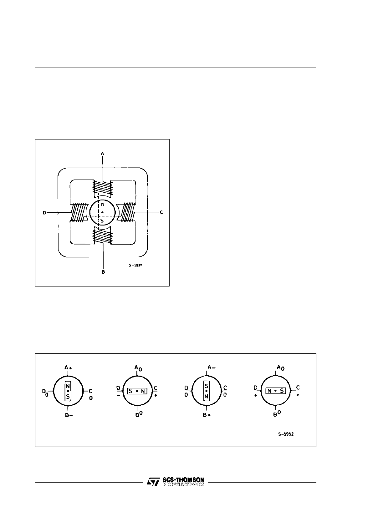
BIPOLAR STEPPER MOTOR BASICS
Simplified to the bare essentials, a bipolar permanent magnet motor consists of a rotating-permanent magnet surrounded by stator poles carrying
the windings (fig. 5).
Figure 5: Simplified Bipolar Two Phase Motor
Bidirectional drive current is imposed on windings
A-B and C-D andthe motor is stepped by commutating the voltage applied to the windings in sequence. For a motor of this type there are three
possible drive sequences.
Figure 6: One-Phase-on (Wave Mode) Drive
One-Phase-on or Wave Drive
Only one winding is energized at any given time
according to thesequence :
AB - CD - BA - DC
(BAmeans that the current is flowing from Bto A).
Fig.6 showsthe sequence for a clockwiserotation
and the corresponding rotor position.
Two-Phase-on or NormalDrive
Thismode givesthe highesttorque sincetwo windings are energized at any given time according to
the sequence (for clockwiserotation).
AB & CD ; CD & BA; BA & DC; DC & AB
Fig. 7 shows the sequenceand the corresponding
positionof the rotor.
Half Step Drive
This sequence halves the effective step angle of
the motorbut gives aless regular torque being one
winding or two windings alternatively energized.
Eight steps are required for a complete revolution
of the rotor.
The sequence is:
AB ; AB& CD ; CD ; CD & BA; BA; BA& DC;
DC ; DC& AB
as shown in fig. 8.
By theconfigurations of fig. 6, 7,8 the motor would
have astep angle of90 ° (or 45° inhalf step). Real
motorshave multiplepoles pairsto reducethe step
angle to a fewdegrees but the number of windings
(two) and the drive sequence are unchanged.
GS-D200/GS-D200S

7/17
Figure 7: Two-Phase-on(Normal Mode) Drive
Figure 8: Half Step Sequence
GS-D200/GS-D200S

8/17
PHASE SEQUENCE GENERATION INSIDE THE
GS-D200/GS-D200S
The modules contains a three bit counter plus
some combinational logic which generate suitable
phase sequences for half step, wave and normal
full step drive. This3 bit countergenerates a basic
eight-step Gray code master sequence as shown
in fig. 9. To select thissequence, that corresponds
to half step mode, the HALF/FULL input (pin 4)
must be kept high or unconnected.
The full step mode (normal and wave drive) are
both obtainedfrom theeightstep mastersequence
by skipping alternate states. This is achieved by
forcing the step clock to bypass the first stage of
the 3 bit counter. The least significant bit of this
counteris not affectedandtherefore the generated
sequence depends on the state of the counter
when full step mode is selected by forcing pin 4
(HALF/FULL)low. If full step isselected when the
counter is at any odd-numbered state, the twophase-on (normal mode) is implemented (see fig.
10).
On the contrary, if the full mode is selected when
the counter is at an even-numbered state, the
one-phase-on (wave drive) is implemented (see
fig. 11).
Figure 9: The Eight Step Master Sequence corresponding to Half Step Mode.
GS-D200/GS-D200S

9/17
Figure 10: Two-Phase-on (NormalMode) Drive Figure 11: One-Phase-on (Wave Mode) Drive
RESET, ENABLE AND HOME SIGNALS
The RESET is an asynchronous reset input which
restores the module to the home position (state1 :
ABCD= 0101). Resetis activewhen low.
The HOME output signals this condition and it is
intendedto beANDed withthe outputofa mechanical home position sensor.
The ENABLEinput is used to start up the module
after the system initialization. ENABLE is active
when high or unconnected.
MOTOR CURRENT REGULATION
The two bipolar winding currents are controlled by
two internal choppers in a PWM mode to obtain
good speed andtorque characteristics.
An internaloscillatorsuppliespulses atthe chopper
frequency to both choppers.
When the outputs areenabled, the currentthrough
the windings raises until a peak value set by I
oset
and R
sense
(see the equivalent block diagram) is
reached. At this moment the outputs are disabled
andthe currentdecaysuntilthe nextoscillatorpulse
arrives.
The decay time of the current can be selected by
theCONTROLinput(pin 10). Ifthe CONTROLinput
is kept high or openthe decay is slow,as shownin
fig. 12, where the equivalent power stage of GSD200, the voltages on A and B are shown as well
as the current waveform on winding AB.
When the CONTROLinput is forcedlow, the decay
is fast as shown in fig. 13.
The CONTROL input isprovided on GS-D200 and
GS-D200S to allow maximum flexibility in application.
If the modules must drive a large motor that does
not store muchenergy inthe windings, the chopper
frequency must be decreased: this is easily obtainedby connecting an externalcapacitorbetween
OSC pin and GND1.
In these conditions a fastdecay (CONTROLLOW)
would imposea low averagecurrent andthe torque
could be inadequate. By selecting CONTROL
HIGH, the average current is increased thanks to
the slow decay.
When the GS-D200S is used in the fast-decay
mode it is recommended to connect external fast
recovery, low drop diodes between each phase
output and the supply return (GND). The slow-decay should be the preferredoperating recirculation
mode because of the lower power dissipation and
low noise operations.
GS-D200/GS-D200S

10/17
Figure 12: Chopper Control with Slow Decay
Figure 13: Chopper Control with Fast Decay
drivecurrent(Q1,Q2ON)
––––recirculation current
(Q
1
ON,Q2OFF,D1ON)
drivecurrent (Q
1,Q2
ON)
– – – – recirculation current
(Q
1,Q2
OFF,D1,D2ON)
GS-D200/GS-D200S

11/17
USER NOTES
Supply Voltage
The recommended operating maximum supply
voltage must include the ripple voltage for the V
s
rail, and a 5V±5% for the Vssline is required.
The two supply voltages must to be correctly sequenced to avoidany possible erroneous positioning of the power stages.The correctpower-up and
power-down sequences are:
Power-up 1) Vss(5V) is applied with Enable =Low
2) Vs (the motor supply voltage)
is applied
3) Enable is brougth High
Power-down 1) Enable is brougth Low
2) Vsis switched off
3) Vssis switched off.
Case Grounding
The module case is internally connected to pin 1
and 13. To obtain additional effective EMI shield,
the PCB areabelow the modulecan be used as an
effective sixth side shield.
Thermal Characteristics
The case-to-ambient thermal resistanceof the GSD modules is 5°C/W. This produces a 50°C temperature increase of the modulesurface for 10Wof
internal dissipation.
According to ambient temperature and/or to power
dissipation, an additional heatsink or forced ventilation may berequired. (See derating curves).
Supply Line Impedance
The module has an internal capacitor connected
accross the supply pins (18 and 13) to assure the
circuit stability. This capacitor cannot handle high
values of currentripple, andwould be permanently
damaged if the primary energy source impedance
is not adequate.
The use of a low ESR, high ripple current 470µF
capacitor located as close to the module as possible is recommended. Suitable units are the SPRAGUE type 672D, the SPRAGUE 678D, the RIFA
type PEG 126 or any equivalent unit. When space
is a limitation, a 22µF ceramic multilayer capacitor
connected across the module input pins must be
used.
Module Protections
The GS-D200 outputs are protected against occasional and permanent short-circuits of the output
pin to the supply voltage. The GS-D200S outputs
are also protected against short circuits to ground
and to another output. When the current exceeds
the maximum value, the output is automatically
disabled.
The GS-D200S protection is of the latching type,
i.e. when an overload condition is detected the
unit outputs are disabled. To restart the operations it is necessary to disable the unit (pin
11=Low) or to switch off the supply voltage for at
least 100ms.
Motor Connection
The motorisnormally quitefar fromthe moduleand
long cables are needed for connection. The use of
a twistedpair cable with appropriate cross section
for eachmotor phase isrecommended to minimize
DC losses and RFIproblems.
Unused Inputs
All the GS-D200 and GS-D200S logic inputs have
an internal pull-up, andthey are highwhen unconnected.
Phase Current Programming
The output current of the GS-D200is factoryset to
1A while the GS-D200S has a standard 2A value.
The phase current value can be changed by connecting an appropriate resistor between pin 9 and
ground or Vss(see fig. 14). In the first case the
phase current will decrease, in the latter it will
increase.
The maximum phase current must be limited to 2A
for the GS-D200 and 2.5A for the GS-D200S to
avoid permanent damage to the module.
GS-D200 phase current programming:
I>1A Ri =
10 − I
0.993 ⋅ I− 1
= kΩ Ri≥ 8.2 kΩ
I<1A Rd =
I
1− 0.993 ⋅ I
=kΩ
GS-D200Sphase currentprogramming:
I>2A Ri =
10 − 0.33 ⋅I
0.473 ⋅ I− 1
= kΩ Ri≥ 50 kΩ
I<2A Rd =
I
3.03 − 1.43 ⋅ I
= kΩ
GS-D200/GS-D200S

12/17
12
9
1
12
9
1
Figure 14: GS-D200 and GS-D200S Phase Current Programming
12
8
1
12
8
1
oscosc
fC< 17 KHz
fC>17KHz
Figure 15: Chopper Frequency Programming
Chopper Frequency Programming
The chopper frequency is internally set to 17kHz,
and it can be changed by addition of external
components as follows. To increase the chopper
frequency a resistor must be connected between
Oscillator (pin 8) and Vss(pin12, see fig. 15).
The resistor value is calculated according to the
formula:
Rf =
306
fc − 17
= kΩ where fc = kHz Rf≥ 18kΩ
To decrease the chopper frequency a capacitor
must be connected between Oscillator(pin 8) and
Gnd1 (pin 1). The capacitor value is calculated
according to theformula:
Cf =
80.5 − 4.7fc
fc
= nF where fc = kHz
GS-D200/GS-D200S

13/17
Figure 16: GS-D200 Free Air Derating Curve Figure 17: GS-D200S Free Air Derating Curve
MULTI MODULES APPLICATION
Incomplex systems, many motors mustbe controlled and driven. In such a case more than one
GS-D200 or GS-D200 S mustbe used.
To avoid chopper frequencies noise and beats, all
the modules shouldbe synchronized.
If all the motors are relatively small, thefast decay
maybe used, thechopper frequency does notneed
any adjustementand fig.18 shows howto synchronize several modules.
When at least one motor is relatively large a lower
chopper frequency and a slow decay may be required: In such a case the overall system chopper
frequency is determined bythe largestmotor in the
system as shown in fig. 19.
Figure 18: Multimotor Synchronization. Small Motor and Fast CurrentDecay
Tamb(°C)
Tamb(°C)
GS-D200/GS-D200S

14/17
Figure 19: Multimotor Synchronization. Large and Small Motor. Slow Current Decay
THERMAL OPERATING CONDITIONS
In many cases the modules do not require any
additional coolingbecause the dimensions and the
shape of the metal box are studied to offer the
minimum possible thermal resistance case-to-ambient for a given volume.
It should be remembered that these modules area
power deviceand, depending onambient temperature, an additional heath-sink or forced ventilation
or bothmay be requiredto keep the unitwithin safe
temperature range. (Tcase
max
<85°C during op-
eration).
The concept of maximum operating ambient tem-
perature is totally meaningless when dealing with
power components because the maximum operating ambienttemperature depends on how a power
device is used.
What can be unambiguously defined is the case
temperature of the module.
To calculate the maximumcase temperature of the
module in a particular applicative environment the
designer must know the following data:
– Input voltage
– Motor phase current
– Motor phase resistance
– Maximum ambient temperature
From thesedata itis easy to determinewhether an
additional heath-sink is required or not, and the
relevant size i.e. the thermal resistance.
The stepby stepcalculation isshown for thefollowing example (GS-D200).
Vin=40V,I
phase
= 1 A, RphPhase resistance =
=10Ω, max. TA=50°C
● Calculate the power dissipated from the indexer
logic and the level shifter (see electrical characteristics):
P
logic
=(5V•60 mA) +(40 V • 20 mA) = 1.1 W
● Calculatetheaverage voltageacross the winding
resistance:
V
out
=(Rph• I
out
)=10Ωζ1A=10V
● Calculatethe required ONdutycycle (D.C.)of the
output stage to obtain the average voltage (this
D.C. is automatically adjusted by the GS-D200):
D.C. =
V
out
V
in
=
10
40
= 0.25
● Calculate the power dissipation of the GS-D200
output power stage. The power dissipation depends on twomain factors:
– the selected operating mode (FAST or SLOW
DECA Y)
– the selected drive sequence (WAVE, NORMAL,
HALF STEP)
FAST DECAY. For this mode of operation, the
internal voltage drop isVsat
source
+Vsat
sink
during
the ON period i.e. for 25 % of the time.
During the recirculation period (75 % of the time),
the current recirculates on two internal diodes that
have avoltage dropVd=1 V,andtheinternal sense
resistor (0.5 Ω). For this example, by assuming
maximum values for conservative calcu lations,the
power dissipation during one cycle is:
Ppw= 1.1 • [2 V
sat
• Iph• D.C.+ 2 Vd• Iph•
(1 - D.C.)+ 0.5 • Iph]
GS-D200/GS-D200S

Ppw=1.1•[2•1.8•1•0.25+2•1•1•0.75 + 0.5 • 1]
Ppw=1.1•[0.9 + 1.5 + 0.5] = 3.19 W
The factor 1.1 takes into account the power dissi-
pation during the switching transient.
SLOW DECAY. The power dissipation during the
ON period is the same. The RECIRCULATION is
made internally t hrough a power transistor
(V
satsink
) and a diode. The power dissipation is,
therefore:
Ppw= 1.1•[2 V
sat•Iph
•D.C.+(V
sat+Vd
)•I
ph
•(1-D.C.)]
Ppw=1.1•[2•1.8 •1•0.25 + (1.8+ 1) • 1 • 0.75]
Ppw=1.1•[0.9 + 2.1] = 3.3 W
WAVE MODE. When operating in this mode the
power dissipation is given by values of FASTand
SLOW DECAYmode, because one phase is energized at any given time.
NORMALMODE. At any given time, two windings
are alwaysenergized. The powerdissipation ofthe
power output stage is therefore multiplied by a
factor 2.
HALF STEP. The power sequence, one-phase-on,
two-phase-on forces the power dissipation to be
1.5 times higher than in WAVE MODE when the
motor is running. In stall condition the worst case
for power dissipation is with two-phase-on i.e. a
powerdissipation as in NORMAL MODE.
The following tablesummarizes the power dissipations of the output power stage of the GS-D200
when running for this example:
Wave Normal Half Step
Fast Decay
3.19W 6.38 W 6.38W
Slow Decay
3.30W 6.60 W 6.60W
● Calculate the total power dissipation for the GS-
D200 :
P
tot=Plogic+Ppw
In this example, for slow decay and normal mode
P
tot
= 1.1 +6.6 =7.7 W
● The case temperature can now be calculated:
T
case=Tamb
+(P
tot•Rth
) = 55 + (7.7 • 5) = 93.5 °C
● If the calculated case temperature exceeds the
maximum allowed case temperature, as in this
example,an externalheat-sink is required and the
thermalresistance canbe calculated according to:
Rth
tot
=
T
cmax
− Tamb
P
tot
=
85 − 55
7.7
= 3.9°C
and then
Rthhs=
Rth ⋅ Rth
tot
Rth − Rth
tot
=
5 ⋅ 3.9
5 − 3.9
= 17.7°C
The following table gives the thermal resistanceof
some commerciallyavailable heath-sinksthat fit on
the GS-D200 module.
ManufacturerPart Number Rth(°C/W) Mounting
Thermalloy
6177 3 Horizontal
Thermalloy
6152 4 Vertical
Thermalloy
6111 10 Vertical
Fischer
SK18 3 Vertical
Assman
V5440 4 Vertical
Assman
V5382 4 Horizontal
15/17
GS-D200/GS-D200S

MECHANICAL DATA
2.54 (0.1)
5.04 (0.2)
5.04 (0.2)
5.04 (0.2)
2.54 (0.1)
2.54 (0.1)
18.4
(0.72)
29.5
(1.16)
2.2 (0.87)
2.2 (0.87)
1.2 (0.47)
66.67 (2.62)
78.5 (3.09)
82.3 (3.24)
85.5 (3.37)
18.5 (0.73)
20.5 (0.81)
0.5 (0.02)
7 (0.28)
23.0
(0.90)
4 (0.16)
Dimensions in mm
MOTHER BOARD LAYOUT
16/17
GS-D200/GS-D200S

17/17
Information furnished is believed to be accurate and reliable. However, SGS-THOMSON Microelectronics assumes no responsibility for the
consequences of use of such information nor for any infringement of patents or otherrights of third parties which may result from its use. No
license is granted by implicationor otherwise under any patent or patent rights of SGS-THOMSONMicroelectronics.Specification mentioned
in this publication are subject to change without notice. This publication supersedes and replaces all information previously supplied.
SGS-THOMSONMicroelectronics products are not authorized for use as critical components in lifesupport devices or systems without express
written approval of SGS-THOMSON Microelectronics.
1994 SGS-THOMSON Microelectronics – All Rights Reserved
SGS-THOMSON MicroelectronicsGROUP OF COMPANIES
Australia - Brazil - China - France - Germany - Hong Kong- Italy- Japan- Korea - Malaysia - Malta - Morocco - The Netherlands-
Singapore- Spain - Sweden- Switzerland- Taiwan- Thailand - United Kingdom - U.S.A.
GS-D200/GS-D200S
 Loading...