

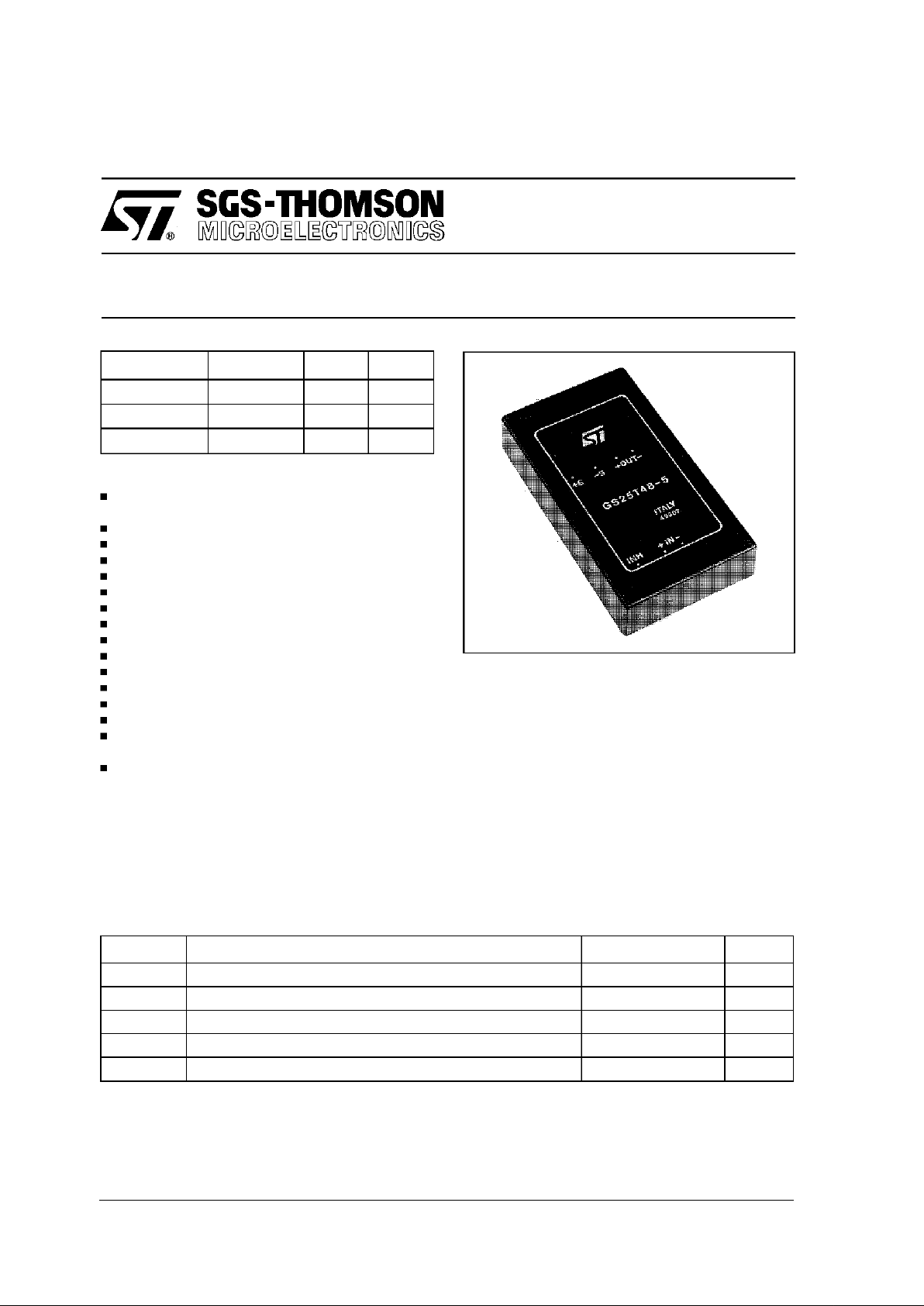
GS25/30T48 Family
25/30 W DC-DC CONVERTER FAMILY
December 1993 1/5
Type V
in
V
out
I
out
GS25T48-5 36 to 72 V 5 V 5 A
GS25T48-12 36 to 72 V 12 V 2,5A
GS25T48-15 36 to 72 V 15 V 2 A
FEATURES
MTBF in excess of 1M hours at +45°C ambient
temperature
Wide inputvoltagerange(36to 72V)
No external componentrequired
High efficiency(see data)
Non latchingpermanent short-circuitprotection
Overvoltageprotection
Redundantoperation
Remoteoutput voltage sense
RemoteINHIBIT/ENABLE
Soft-start
Minimizedreflected input current
Reverseinput polarity protection
Peakinput overvoltage withstand
No derating over the temperaturerange
500V
DC
minimum isolation between input and
output
PCB or chassismountable
DESCRIPTION
The GS25T48-5, GS30T48-12 and GS30T48-15
are isolated DC-DC converters designed for general purpose application.
The output poweris in the range of 25W to 30W.
To ensure very long life, these converters do not
use electrolytic aluminum capacitors or optoelectronic feedbacksystems.
ABSOLUTEMAXIMUM RATINGS
Symbol Parameter Value Unit
V
i
DC Input Voltage
34 to 72V V
V
ipk
Input Transient Overvoltage (t ≤ 1sec.)
90 V
V
ir
Input Reverse Voltage
100 V
T
stg
Storage Temperature Range
-55 to +105 °C
T
op
Operating Temperature Range
-25 to +71 °C

2/5
ELECTRICALCHARACTERISTICS (T
amb
=25°C unlessotherwise specified)
Symbol
Parameter Test Conditions Min Typ Max Unit
V
i
Input Voltage Full Load
36 48 72 V
I
i
Input Current GS25T48-5
Full Load 640 mA
GS30T48-12
Full Load 730
GS30T48-15
Full Load 730
I
ir
Input Reflected
Current
Vi= 48V
Full Load 50 mApp
I
isc
Input Short-circuit
Current
GS25T48-5
Vi= 48V
710 mA
GS30T48-12
Vi= 48V
820
GS30T48-15
Vi= 48V
820
l
iq
Input Quiescent
Current
Vi= 48V
Converter OFF
5mA
V
inhl
Low Inhibit Voltage Vi= 48V
Full Load 1.2 V
V
inhh
High Inhibit Voltage Vi= 48V
Full Load
1.8
(open)
V
l
inh
Input Inhibit Current Vi= 48V
Full Load 1 mA
V
o
Output Voltage
GS25T48-5
Vi= 48V
Full Load
4.95 5.00 5.05
V
GS30T48-12
Vi= 48V
Full Load
11.88 12.00 12.12
GS30T48-15
Vi= 48V
Full Load
14.85 15.00 15.15
V
or
Output Ripple and
Noise Voltage
Vi= 48V
Full Load
10 mVpp
δV
o
Line Regulation
Vi= 36 to 72V
Full Load
±0.001 %
δV
o
Load Regulation
Vi= 48V
Full Load to No Load
±0.05 %
V
oov
Output Overvoltage
Protection
GS25T48-5
Vi= 48V
Full Load 6.8 V
GS30T48-12
Vi= 48V
Full Load 15
GS30T48-15
Vi= 48V
Full Load 18
δVo
Remote Sense per Leg Vi= 36V
0.5 V
Tc
Temperature
Coefficient
Vi= 48V Full Load
Operating Temperature Range
+0.02 %/°C
GS25/30T48 FAMILY

Symbol
Parameter Test Conditions Min Typ Max Unit
I
o
Output Current
GS25T48-5
Vi=36to72V
05A
GS30T48-12
Vi=36to72V
0 2.5
GS30T48-15
Vi=36to72V
02
I
osck
Output Current Limit
GS25T48-5
Vi= 48V
Overload
5.5 A
GS30T48-12
Vi= 48V
Overload
2.75
GS30T48-15
Vi= 48V
Overload
2.2
t
ss
Soft-start Time Vi= 48V
Full Load 30 ms
t
rt
Transient Recovery
Time
Vi= 48V
Step Load Change δIo = 25%
75 µs
V
is
Isolation Voltage
500 Vdc
R
is
Isolation Resistance
10
9
Ω
f
s
Switching Frequency
150 kHz
η
Efficiency
GS25T48-5
Vi= 48V
Full Load
81 %
GS30T48-12
Vi= 48V
Full Load
86
GS30T48-15
Vi= 48V
Full Load
86
R
thc
Thermal Resistance
Case to Ambient
4 °C/W
ELECTRICALCHARACTERISTICS (T
amb
=25°C unlessotherwise specified) (cont’d)
3/5
GS25/30T48 FAMILY

PackageF. Dimensionsin mm. (inches)
CONNECTIONDIAGRAM AND MECHANICAL DATA
4/5
PIN DESCRIPTION
Pin Function Description
1
-IN Negative input voltage.
2
+IN
Positive input voltage. Unregulated input voltage (typically 48V) must be applied between
pins 1-2. The input section of the DC-DC converter isprotected against reverse polarity by
a series diode. No external fuse is required. Input is filtered by a Pi network.
3
ON/OFF
Logically compatible with CMOS or open collector TTL. The converter is ON (Enable)
when the voltage applied to this pin with reference to pin 1 is higher than 1.8V.The
converter is OFF (Inhibit) for a control voltage lower than 1.2V.When the pin is
unconnected the converter is ON (Enable).
4
+ SENSE
Senses the remote load high side. Tobe connected to pin 6 when remote sense is not
used.
5
-SENSE Senses the remote load return. Tobe connected to pin 7 when remote sense is not used.
6
+ OUT Output voltage.
7
-OUT Output voltage return.
GS25/30T48 FAMILY

5/5
Information furnished is believed to be accurate and reliable. However, SGS-THOMSON Microelectronics assumes no responsibility for the
consequences of use of such information nor for any infringement of patents or other rights of third parties which may result from its use. No
license is granted by implication or otherwiseunder any patent or patent rights of SGS-THOMSON Microelectronics. Specification mentioned
in this publication are subject to change without notice. This publication supersedes and replaces all information previously supplied.
SGS-THOMSON Microelectronics products are not authorized for use ascritical componentsin life support devices or systems without express
written approval of SGS-THOMSON Microelectronics.
1994 SGS-THOMSON Microelectronics – All Rights Reserved
SGS-THOMSON Microelectronics GROUP OF COMPANIES
Australia - Brazil - France - Germany - Hong Kong - Italy - Japan -Korea - Malaysia - Malta - Morocco - The Netherlands -
Singapore - Spain - Sweden - Switzerland - Taiwan- Thailand - United Kingdom - U.S.A.
GS25/30T48 FAMILY
 Loading...