

Datasheet GS175T48-15, GS175T48-12, GS175T48-5, GS120T48-3.3 Datasheet (SGS Thomson Microelectronics)
GS120/175T48 Family
120W/175W DC-DC CONVERTERS FAMILY
Type V
GS120T48-3.3
GS120T48-3.3E
GS175T48-5
GS175T48-5E
GS175T48-12
GS175T48-12E
GS175T48-15
GS175T48-15E
i
38 to 60 V 3,35 V 35 A
38 to 60 V 5,075 V 35 A
38 to 60 V 12,0 V 15 A
38 to 60 V 15,0 V 12 A
V
o
I
FEATURES
UL, CSA, TUVapproved
High outputpower (up to 175W)
High efficiency(82% typ. on GS175T48-5module)
Paralleloperation with equal current sharing
Synchronizationpin
Remote ON/OFF
Remote load voltagesense compensation
Output short-circuitprotection
Undervoltagelock-out
Minimal overshootduring load transients
Output overvoltageprotection
500V
inputto output isolationvoltage
DC
Internal input and output filtering
Softstart
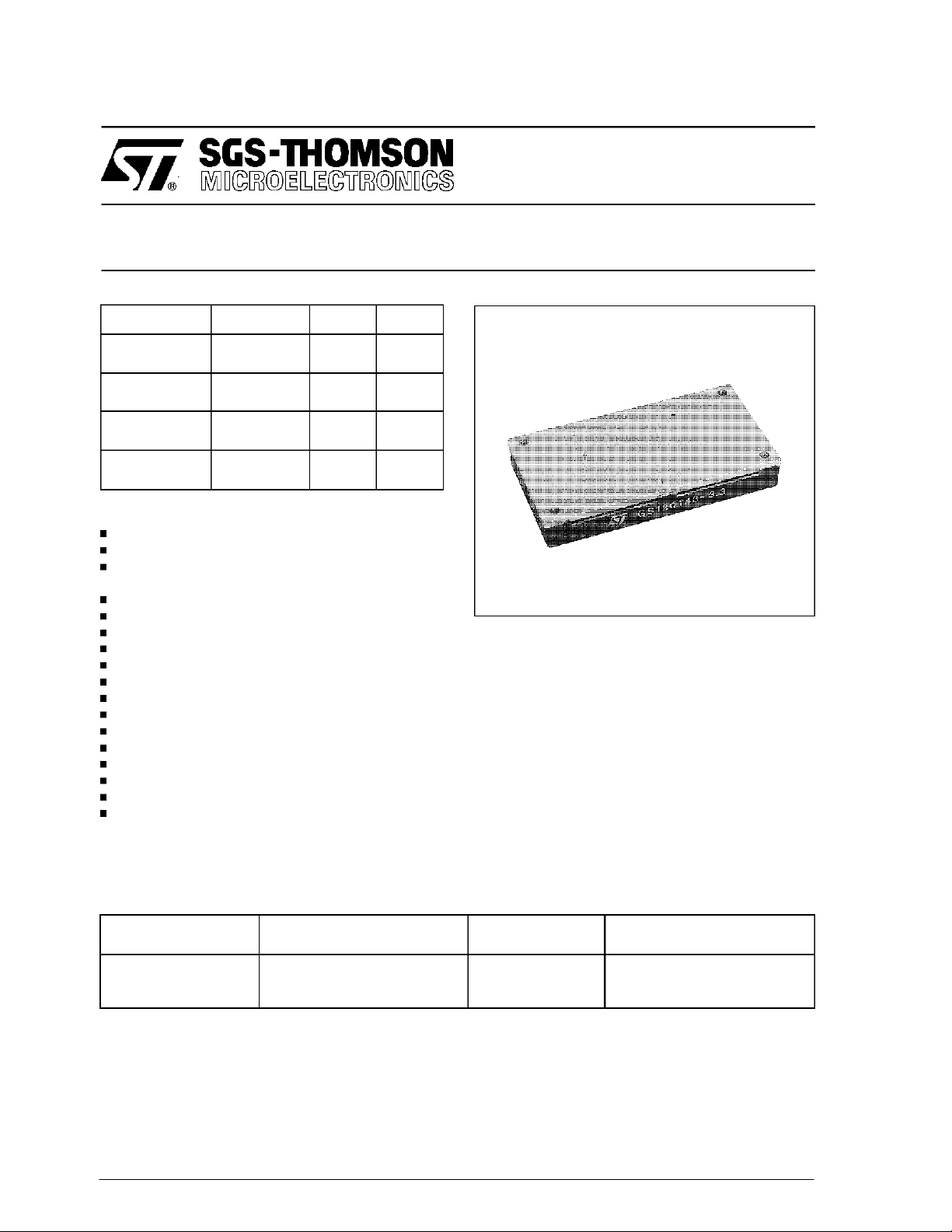
PCB or chassismountable
Optional additional finned heatsink
Mechanical dimensions 125 • 66,5 • 19 (4,92 •
2,62 • 0,75)
o
DESCRIPTION
The GS120/175T48familyincludes120/175WDCDC convertersused to generate fixed isolatedoutput voltages with an outputcurrent up to 35A from
a wide range input voltage (38 to 60V).
The suffix E Identifies the metric threading on the
planar heatsink (see fig. 1).
OPTION
Type
Ordering Number
HS01
June 1994 1/10
Description Thermal Resistance
Additional finned heatsink
(See fig. 7)
2.8°C/W
Dimensions
L • W• H mm (inches)
125 • 66.5 • 15
( 4.92 • 2.62 • 0.59)

GS120/175T48 FAMILY
GS120T48-3.3ELECTRICAL CHARACTERISTICS (T
Symbol Parameter Test Conditions Min Typ Max Unit
Input Voltage Vo= 3.35V Io= 0 to 35A
V
i
V
l
ipk
V
l
ien
V
V
V
V
V
V
V
∆V
δV
I
I
osc
t
V
R
T
cop
T
Input Undervoltage Lockout Vo= 3.35V
iuv
AverageInput Current Vi= 0 to 60V
l
i
Inrush Transient Peak Current Vi= 60V
Reflected Input Current Vi= 38 to 60V
l
ir
Enable Input Voltage Vi= 38 to 60V Io= 0 to 35A
ien
Enable Input Current Vi= 38 to 60V Io= 0 to 35A
Inhibit Voltage Vi= 38 to 60V Io= 0 to 35A
iinh
Input Power Vi= 38 to 60V Io= 0A (No Load)
P
i
Total Output Voltage Regulation Vi= 38 to 60V Io= 0 to 35A
o
Short-term Output
ost
VoltageRegulation
Total Static Tolerance Vi= 38 to 60V Io= 0 to 35A
ots
Output Overvoltage
ol
Limit Initiation
Output Ripple Voltage Vi= 38 to 60V Io= 35A
or
Output Noise Voltage Vi= 38 to 60V Io= 35A
on
Total RemoteSense
o
Compensation
Peak Load Transient Response Vi= 48V δIo=5A
o
Output Current Vi= 38 to 60V Vo= 3.35V
I
o
OvercurrentLimit Initiation Vi= 48V
ol
Shortcircuit Output Current Vi= 48V
LoadTransient Settling Time Vi= 48V δIo=5A
t
s
Turn-onTime Vi= 48V Io= 35A
on
IsolationVoltage
is
Switching Frequency Vi= 38 to 60V Io= 0 to 35A
f
s
η Efficiency V
Thermal Resistance Case toAmbient
th
Operating Case
Temperature Range
Storage Temperature Range
stg
(Operating Conditions)
Io= 0 to 35A
Io= 35A
Io= 35A
BW = 5Hz to 20MHz
Io= 35A (See fig. 2)
V
=0V
ien
Vien = open
Vi= 38 to 60V Io= 0 to 35A
Vi= 38 to 60V Io= 0 to 35A
Vi= 38 to 60V
slope = 0.1A/µs
Vo= 0.2 to 0.5V
slope = 0.1A/µs
V
= from high to low
ien
V
= 0 to 60V Io= 35A
i
V
= low
ien
= 38 to 60V Io= 35A
i
=25°Cunless otherwisespecified)
amb
38 48 60 V
32 34 36 V
0 1.2 V
818V
1.5 2 W
3.25 3.35 3.45 V
3.30 3.35 3.40 V
3.28 3.35 3.42 V
4 4.5 5.2 V
20 30 mVpp
50 80 mVpp
035A
36 39 A
310
500 V
160 175 200 kHz
76 77 %
5.2 °C/W
– 10 +85 °C
– 40 +105 °C
4.2 A
0.2 A
20 mApp
-1 mA
0.6 V
60 mVp
51 A
200 µs
5ms
DC
DC
2
DC
s
2/10
GS120/175T48 FAMILY
GS175T48-5ELECTRICAL CHARACTERISTICS (T
Symbol
Input Voltage Vo= 5.075V Io= 0 to 35A
V
i
V
l
ipk
V
l
ien
V
V
V
V
V
V
V
∆V
δV
I
I
osc
t
V
R
T
cop
T
Input Undervoltage Lockout Vo= 5.075V
iuv
AverageInput Current Vi= 0 to 60V Io= 35A
l
i
Inrush Transient Peak Current Vi= 60V
Reflected Input Current Vi= 38 to 60V
l
ir
Enable Input Voltage Vi= 38 to 60V Io= 0 to 35A
ien
Enable Input Current Vi= 38 to 60V Io= 0 to 35A
Inhibit Voltage Vi= 38 to 60V Io= 0 to 35A
iinh
Input Power Vi= 38 to 60V Io= 0A (No Load)
P
i
Total Output Voltage Regulation Vi= 38 to 60V Io= 0 to 35A
o
Short-term Output
ost
VoltageRegulation
Total Static Tolerance Vi= 38 to 60V Io= 0 to 35A
ots
Output Overvoltage
ol
Limit Initiation
Output Ripple Voltage Vi= 38 to 60V Io= 35A
or
Output Noise Voltage Vi= 38 to 60V Io= 35A
on
Total RemoteSense Compensation Vi= 38 to 60V
o
Peak Load Transient Response Vi= 48V δIo=5A
o
Output Current Vi= 38 to 60V Vo= 5.075V
I
o
OvercurrentLimit Initiation Vi= 48V
ol
Shortcircuit Output Current Vi= 48V
LoadTransient Settling Time Vi= 48V δIo=5A
t
s
Turn-onTime Vi= 48V Io= 35A
on
IsolationVoltage
is
Switching Frequency Vi= 38 to 60V Io= 0 to 35A
f
s
η Efficiency V
Thermal Resistance Case toAmbient
th
Operating Case
Temperature Range
Storage Temperature Range
stg
Parameter Test Conditions Min Typ Max Unit
(Operating Conditions)
Io= 0 to 35A
Io= 35A
BW = 5Hz to 20MHz
Io= 35A (See fig. 2)
V
=0V
ien
Vien = open
Vi= 38 to 60V Io= 0 to 35A
Vi= 38 to 60V Io= 0 to 35A
slope = 0.1A/µs
Vo= 0.2 to 0.5V
slope = 0.1A/µs
V
= from high to low
ien
V
= 0 to 60V Io= 35A
i
V
= low
ien
= 38 to 60V Io= 35A
i
=25°C unlessotherwise specified)
amb
38 48 60 V
32 34 36 V
0 1.2 V
818V
4.94 5.075 5.21 V
5.002 5.075 5.148 V
4.97 5.075 5.18 V
6 6.3 7 V
035A
36 39 A
310
500 V
160 175 200 kHz
81 82 %
– 10 +85 °C
– 40 +105 °C
DC
DC
6.1 A
2
0.2 A
30 mApp
-1 mA
1.5 2 W
20 30 mVpp
50 80 mVpp
0.6 V
100 mVp
51 A
250 µs
5ms
5.2 °C/W
s
DC
3/10

GS120/175T48 FAMILY
GS175T48-12ELECTRICAL CHARACTERISTICS (T
Symbol
Input Voltage Vo= 12V Io= 0 to 15A
V
i
V
l
ipk
V
l
ien
V
V
V
V
V
V
V
∆V
δV
I
I
osc
t
V
R
T
cop
T
Input Undervoltage Lockout Vo= 12V
iuv
AverageInput Current Vi= 0 to 60V Io= 15A
l
i
Inrush Transient Peak Current Vi= 60V
Reflected Input Current Vi= 38 to 60V
l
ir
Enable Input Voltage Vi= 38 to 60V Io= 0 to 15A
ien
Enable Input Current Vi= 38 to 60V Io= 0 to 15A
Inhibit Voltage Vi= 38 to 60V Io= 0 to 15A
iinh
Input Power Vi= 38 to 60V Io= 0A (No Load)
P
i
Total Output Voltage Regulation Vi= 38 to 60V Io= 0 to 15A
o
Short-term Output
ost
VoltageRegulation
Total Static Tolerance Vi= 38 to 60V Io= 0 to 15A
ots
Output Overvoltage
ol
Limit Initiation
Output Ripple Voltage Vi= 38 to 60V Io= 15A
or
Output Noise Voltage Vi= 38 to 60V Io= 15A
on
Total RemoteSense
o
Compensation
Peak Load Transient Response Vi= 48V δIo=3A
o
Output Current Vi= 38 to 60V Vo= 12V
I
o
OvercurrentLimit Initiation Vi= 48V
ol
Shortcircuit Output Current Vi= 48V
LoadTransient Setting Time Vi= 48V δIo=3A
t
s
Turn-onTime Vi= 48V Io= 15A
on
IsolationVoltage
is
Switching Frequency Vi= 38 to 60V Io= 0 to 15A
f
s
η Efficiency V
Thermal Resistance Case toAmbient
th
Operating Case
Temperature Range
Storage Temperature Range
stg
Parameter Test Conditions Min Typ Max Unit
(Operating Conditions)
Io= 0 to 15A
Io= 15A
BW = 5Hz to 20MHz
Io= 15A (See fig. 2)
V
=0V
ien
Vien = open
Vi= 38 to 60V Io= 0 to 15A
Vi= 38 to 60V Io= 0 to 15A
Vi= 38 to 60V
slope = 0.2A/µs
slope = 0.2A/µs
V
= from high to low
ien
V
= 0 to 60V Io= 15A
i
V
= low
ien
= 38 to 60V Io= 15A
i
=25°C unless otherwisespecified)
amb
38 48 60 V
32 34 36 V
0 1.2 V
818V
1.5 2 W
11.4 12.0 12.6 V
11.76 12.0 12.24 V
11.64 12.0 12.36 V
13.2 14 15 V
015A
16 19 A
310
500 V
160 175 200 kHz
84 86 %
5.2 °C/W
– 10 +85 °C
– 40 +105 °C
DC
DC
5.5 A
2
0.2 A
20 mApp
-1 mA
35 70 mVpp
60 120 mVpp
0.6 V
200 mVp
25 A
300 µs
5ms
s
DC
4/10

GS120/175T48 FAMILY
GS175T48-15ELECTRICAL CHARACTERISTICS (T
Symbol
Input Voltage Vo= 15V Io= 0 to 12A
V
i
V
l
ipk
V
l
ien
V
V
V
V
V
V
V
∆V
δV
I
I
osc
t
V
R
T
cop
T
Input Undervoltage Lockout Vo= 15V
iuv
AverageInput Current Vi= 0 to 60V Io= 12A
l
i
Inrush Transient Peak Current Vi= 60V
Reflected Input Current Vi= 38 to 60V Io= 12A
l
ir
Enable Input Voltage Vi= 38 to 60V Io= 0 to 12A
ien
Enable Input Current Vi= 38 to 60V Io= 0 to 12A
Inhibit Voltage Vi= 38 to 60V Io= 0 to 12A
iinh
Input Power Vi= 38 to 60V Io= 0A (No Load)
P
i
Total Output Voltage Regulation Vi= 38 to 60V Io= 0 to 12A
o
Short-term Output
ost
VoltageRegulation
Total Static Tolerance Vi= 38 to 60V Io= 0 to 12A
ots
Output Overvoltage
ol
Limit Initiation
Output Ripple Voltage Vi= 38 to 60V Io= 12A
or
Output Noise Voltage Vi= 38 to 60V Io= 12A
on
Total RemoteSense
o
Compensation
Peak Load Transient Response Vi= 48V δIo=3A
o
Output Current Vi= 38 to 60V Vo= 15V
I
o
OvercurrentLimit Initiation Vi= 48V
ol
Shortcircuit Output Current Vi= 48V
LoadTransient Settling Time Vi= 48V δIo=3A
t
s
Turn-onTime Vi= 48V Io= 12A
on
IsolationVoltage
is
Switching Frequency Vi= 38 to 60V Io= 0 to 12A
f
s
η Efficiency V
Thermal Resistance Case toAmbient
th
Operating Case
Temperature Range
Storage Temperature Range
stg
Parameter Test Conditions Min Typ Max Unit
(Operating Conditions)
Io= 0 to 12A
Io= 12A
V
=0V
ien
Vien = open
Vi= 38 to 60V Io= 0 to 12A
Vi= 38 to 60V Io= 0 to 12A
Vi= 38 to 60V
slope = 0.2A/µs
Vo= 0.2 to 0.5V
slope = 0.2A/µs
V
= from high to low
ien
V
= 0 to 60V Io= 12A
i
V
= low
ien
= 38 to 60V Io= 12A
i
=25°C unless otherwisespecified)
amb
38 48 60 V
32 34 36 V
0 1.2 V
818V
1.5 2 W
14.25 15.0 15.75 V
14.7 15.0 15.3 V
14.55 15.0 15.45 V
16.5 17 18 V
012A
13 16 A
310
500 V
160 175 200 kHz
86 88 %
5.2 °C/W
– 10 +85 °C
– 40 +105 °C
DC
DC
5.5 A
2
0.2 A
20 mApp
-1 mA
45 90 mVpp
75 150 mVpp
0.6 V
200 mVp
21 A
300 µs
5ms
s
DC
5/10

GS120/175T48 FAMILY
CONNECTION DIAGRAM AND MECHANICAL DATA
Figure1.
Package T.Dimensions in mm (inches).
PIN DESCRIPTION
Pin Function Description
1-IN
2+IN
3 ON/OFF
4 CASE
5 SYNC
6 PARALLEL
7 + SENSE
8 - SENSE
9,10 - OUT
11,12 + OUT
6/10
Negative input voltage.
Positive input voltage.Unregulated input voltage (typically 48V) mustbeapplied between
pin 1-2.
The converter is ON (Enable) when the voltage applied to this pinwith reference to pin 1 is
lowerthan 1.2V (seeVien). The converter is OFF (Inhibit)for a control voltage in therange
of 8 to 18V. When the pin is unconnected the converter is OFF (Inhibit).
Case connection pin.
Synchronization pin. See figures 3,4, 5, 6. Open when not used.
Parallel output. See figures 3, 4, 5, 6. Open when notused.
Senses the remote load high side. To be connected to pin 11,12when remote sense is not
used.
Senses the remote load return. To be connected to pin 9,10 when remote sense is not
used. In parallel configuration, take care to connect all -S pins together (see figures 3,4,5,6).
Fixed output voltagereturn.
Fixed output voltage.

GS120/175T48 FAMILY
USER NOTES
Reflected Input Current
The reflectedinput current measurement(lir, see ElectricalCharacteristics) is performed according to the
test set-up of fig. 2.
Figure2.
Softstart
To avoid heavy inrush current the output voltage
risetime is 10msmaximuminany conditionof load.
Remote Sensing
The remote voltage sense compensation range is
for a total drop of 0.6V equallysharedbetween the
load connectingwires.
It is a goodpractice to shield the sensing wires to
avoid oscillations.
See the connectiondiagram on figures 3, 4, 5, 6.
Remote ON/OFF
The module is controlled by the voltage applied
between the ON/OFFpin and -IN pin.
The converter is ON (Enable) when the voltage
appliedis lower than 1.2 V (see Vienon Electrical
Characteristics).
The converter is OFF (Inhibit) for a controlvoltage
in the range of 8 to 18V (see Viinh).
When the pinis unconnectedthe converterisOFF.
Maximumsinking current is 1mA.
Module Protection
The module is protected against occasional and
permanent shortcircuits of the output pins to
ground, as well as againstoutputcurrentoverload.
It uses a current limiting protectioncircuitry, avoiding latch-upproblems with certain type of loads.
Acrowbaroutputovervoltageprotectionisactivated
when the output voltage exceeds the specified
values (see ElectricalCharacteristics).
Parallel Operation
To increase available output regulated power, the
module features the parallelconnection possibility
with equalcurrentsharingand maximumdeviation
of 10% (two modules in parallel).
See the connectiondiagramon figures3, 4, 5, 6.
7/10

GS120/175T48 FAMILY
Figure3. Figure 4.
Figure 5.
Finnedheatsink option
An additional finned heatsink is available(type orderingnumberHS01) to allowtheuser to decrease
the total thermal resistance of the module to a
Figure 6.
typical value of 2.8 °C/W. The heatsinkis suitable
both for standard (4-40 UNC threading) and E
version (M3 threading); screw length in the range
of 6 to 8 mm (0.24 to 0.32”). See fig. 7.
8/10

Figure7. - HS01 Heatsink.
GS120/175T48 FAMILY
Dimensions in mm (inches).
Thermal Characteristics
Followingfigures showthebehaviourat stillair and
forced ventilation operation of the GS175T48-5
module (typical efficiency 82%) without
Figure8. - GS175T48-5 with stadard flat heatsink.
(fig.8)andwith theadditionalfinnedHS01heatsink
(fig. 9)
9/10

GS120/175T48 FAMILY
Figure9. - GS175T48-5 with additional HS01 finned heatsink
Safety approvals
Theconverter is agency certifiedto thefollowingsafety requirements.
Agency Requirements License Number
UL UL-STD-1950 E141284
CSA
TUV
UL is a registered trademark of UNDERWRITERS LABORATORIES inc.
CSA isa registered trademark of CANADIAN STANDARDSASSOCIATION.
TUV is a registered trademarkof TUV Rheinland.
Information furnished is believed to be accurate and reliable. However, SGS-THOMSON Microelectronics assumes no responsibility for the
consequences of use of such information nor for any infringement of patents or other rights of third parties which may result from its use. No
license is granted by implicationor otherwise under any patent or patent rights of SGS-THOMSON Microelectronics. Specification mentioned
in this publication are subject to change without notice. This publication supersedes and replaces all information previously supplied.
SGS-THOMSON Microelectronics productsare not authorized foruse ascritical components in life supportdevices orsystems withoutexpress
written approvalof SGS-THOMSON Microelectronics.
1994 SGS-THOMSON Microelectronics – All Rights Reserved
UL is a registered trademark of UNDERWRITERS LABORATORIESinc.
CSA is a registered trademark of CANADIAN STANDARDS ASSOCIATION.
Australia - Brazil - China - France - Germany - Hong Kong - Italy - Japan - Korea - Malaysia - Malta- Morocco - The Netherlands -
Singapore - Spain - Sweden - Switzerland - Taiwan - Thailand - United Kingdom - U.S.A.
CSA-STD-C22.2 No.234
(level 3)
EN 60950
DIN VDE 0805
TUV is aregistered trademark of TUV Rheinland.
SGS-THOMSON Microelectronics GROUP OF COMPANIES
LR 99794-2
R 9272137
10/10
 Loading...