

Datasheet GS70T300-3.5, GS100T300-48, GS100T300-24, GS100T300-15, GS100T300-12 Datasheet (SGS Thomson Microelectronics)
...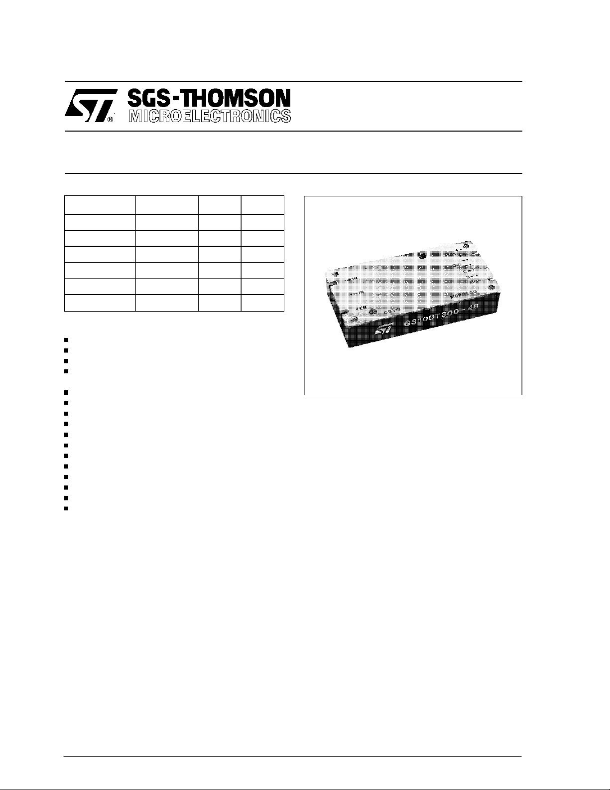
GS70/100T300 Family
70W/100W DC-DC CONVERTERS FAMILY
Type V
GS70T300-3.5 200 to 400 V 3,5 V 20 A
GS100T300-5 200 to 400 V 5,2 V 20 A
GS100T300-12 200 to 400 V 12,0V 8,3 A
GS100T300-15 200 to 400 V 15,0V 6,6 A
GS100T300-24 200 to 400 V 24,0V 4,2 A
GS100T300-48 200 to 400 V 48,0V 2,0 A
i
V
o
I
FEATURES
High inputvoltage range bus: 200 to 400Vdc
UL, TUV approved
High outputpower (up to 100W)
Highefficiency(80%min. onGS100T300-5module)
Outputvoltagesrange:3.5-5.2-12-15-24and 48V
Output voltageadjustable by externalpin
Remote load voltagesense compensation
Output short-circuitprotection
Output overvoltageprotection
Undervoltagelock-out
Minimal overshootduring loadtransients
3750V
input tooutput isolation voltage
RMS
Internal inputand output filtering
Softstart
PCB or chassismountable
Mechanical Dimensions 101,6 • 50,8 • 20 mm
(4,00 • 2,00 • 0,79inches)
o
DESCRIPTION
The GS70/100T300family includes 70/100W DCDC converters used to generate isolated output
voltages with an output current up to 20A from a
wide range input voltage (200 to 400Vdc).
All the GS70/100T300 family modules require an
external fuse (1 Amps.) on the input side.
June 1994 1/10

GS70/100T300 Family
GS70T300-3.5ELECTRICAL CHARACTERISTICS (T
=25°Cunless otherwisespecified)
amb
Symbol Parameter Test Conditions Min Typ Max Unit
V
Q
P
V
V
V
orn
V
δV
δV
∆V
δV
SVR
I
Input Voltage
i
Inrush Charge Vi= 400V
i
Input Power Vi= 300V Io= 0A (No Load)
i
Output Voltage Vi= 200 to 400V
o
Output Voltage Range Vi= 200 to 400V
o
Output Rippleand
Noise Voltage
Output Overvoltage
ol
Limit Initiation
Line Regulation Vi= 200 to 400V
OL
Load Regulation Vi= 300V
OO
Total Remote Sense Compensation Vi= 200 to 400V
o
Peak Load TransientResponse Vi = 300V δIo= 10A
o
Vo= 3.5V Io= 0 to 20A
(Operating Conditions)
Io= 20A
Io=0 to 20A
Io=0 to 20A (see fig. 2)
Vi= 300V
Io= 20A BW = 0 to 20Mhz
Vi= 200 to 400V
Io=0 to 20A
Io= 20A
Io=0 to 20A
Supply VoltageRejection f = 100Hz
Output Current Vi= 200 to 400V
o
Vo= 3.3V
200 300 400 V
-6
40•10
2.5 W
3.43 3.5 3.57 V
1.75 3.5 V
35 40 mVpp
1.2•Vo V
±0.1 %
±0.1 %
0.6 V
500 mVp
55 dB
020A
DC
C
I
I
osc
t
V
OvercurrentLimit Initiation Vi = 300V
oI
Shortcircuit Output Current Vi = 300V
LoadTransient Settling Time Vi= 300V δIo= 10A
t
s
Turn-onTime Vi= 200V Io= 20A
on
IsolationVoltage Input toOutput
is
Switching Frequency Vi= 200 to 400V
f
s
η Efficiency V
Thermal Resistance Baseplate to Ambient
th
Operating Case
Temperature Range
Storage Temperature Range
stg
T
T
R
cop
Input to Baseplate
Output to Baseplate
Io=0 to 20A
= 300V Io= 20A
i
21 23 25 A
18 23 28 A
300 µs
610ms
3750 V
2500
500
150 kHz
78 79 %
7.5 °C/W
0 +70 °C
– 40 +100 °C
RMS
2/10
GS70/100T300 Family
GS100T300-5ELECTRICAL CHARACTERISTICS (T
Symbol
V
i
Q
i
P
i
V
o
V
o
V
orn
V
ol
δV
OL
δV
OO
∆V
o
δV
o
SVR
I
o
Input Voltage
Inrush Charge Vi= 400V
Input Power Vi= 300V Io= 0A (No Load)
Output Voltage Vi= 200 to 400V
Output Voltage Range Vi= 200 to 400V
Output Rippleand
Noise Voltage
Output Overvoltage
Limit Initiation
Line Regulation Vi= 200 to 400V
Load Regulation Vi= 300V
Total Remote Sense Compensation Vi= 200 to 400V
Peak Load TransientResponse Vi = 300V δIo=1A
Supply VoltageRejection f = 100Hz
Output Current Vi= 200 to 400V
Parameter Test Conditions Min Typ Max Unit
Vo=5V Io= 0 to 20A
(Operating Conditions)
Io= 20A
Io=0 to 20A
Io=0 to 20A (see fig. 2)
Vi= 300V
Io= 20A BW = 0 to 20Mhz
Vi= 200 to 400V
Io=0 to 20A
Io= 20A
Io=0 to 20A
Vo=5V
=25°C unless otherwisespecified)
amb
200 300 400 V
40•10
2.5 W
5.09 5.20 5.30 V
2.6 5.20 V
1.2•Vo V
500 mVp
020A
DC
-6
C
40 50 mVpp
±0.1 %
±0.1 %
0.6 V
55 dB
I
I
osc
t
V
OvercurrentLimit Initiation Vi = 300V
oI
Shortcircuit Output Current Vi = 300V
LoadTransient Settling Time Vi= 300V δIo=1A
t
s
Turn-onTime Vi= 200V Io= 20A
on
IsolationVoltage Input toOutput
is
Switching Frequency Vi= 200 to 400V
f
s
η Efficiency Vi
Thermal Resistance Baseplate to Ambient
th
Operating Case
Temperature Range
Storage Temperature Range
stg
T
T
R
cop
Output to Baseplate
Input to Baseplate
Io=0 to 20A
= 300V Io= 20A
21 23 25 A
18 23 28 A
300 µs
610ms
3750 V
500
2500
150 kHz
80 81 %
7.5 °C/W
0 +70 °C
– 40 +100 °C
RMS
3/10

GS70/100T300 Family
GS100T300-12ELECTRICALCHARACTERISTICS (T
Symbol
V
i
Q
i
P
i
V
o
V
o
V
orn
V
ol
δV
OL
δV
OO
∆V
o
δV
o
SVR
I
o
Input Voltage Vo= 12V Io= 0 to 8.3A
Inrush Charge Vi= 400V
Input Power Vi= 300V Io= 0A (No Load)
Output Voltage Vi= 200 to 400V
Output Voltage Range Vi= 200 to 400V
Output Rippleand
Noise Voltage
Output Overvoltage
Limit Initiation
Line Regulation Vi= 200 to 400V
Load Regulation Vi= 300V
Total Remote Sense Compensation Vi= 200 to 400V
Peak Load TransientResponse Vi = 300V δIo=4A
Supply VoltageRejection f = 100Hz
Output Current Vi= 200 to 400V
Parameter Test Conditions Min Typ Max Unit
(Operating Conditions)
Io=8.3A
Io=0 to 8.3A
Io=0 to 8.3A (see fig. 2)
Vi= 300V
Io=8.3A BW = 0 to 20Mhz
Vi= 200 to 400V
Io=0 to 8.3A
Io=8.3A
Io=0 to 8.3A
Vo= 12V
=25°C unless otherwisespecified)
amb
200 300 400 V
40•10
2.5 W
11.76 12.00 12.24 V
6.0 13.2 V
100 120 mVpp
1.2•Vo V
500 mVp
45 dB
0 8.3 A
-6
±0.1 %
±0.1 %
0.6 V
DC
C
I
I
osc
t
V
OvercurrentLimit Initiation Vi = 300V
oI
Shortcircuit Output Current Vi = 300V
LoadTransient Settling Time Vi= 300V δIo=4A
t
s
Turn-onTime Vi= 200V Io= 8.3A
on
IsolationVoltage Input toOutput
is
Switching Frequency Vi= 200 to 400V
f
s
η Efficiency Vi
Thermal Resistance Baseplate to Ambient
th
Operating Case
Temperature Range
Storage Temperature Range
stg
T
T
R
cop
Input to Baseplate
Output to Baseplate
Io=0 to 8.3A
= 300V Io= 8.3A
8.8 9.1 11.0 A
7.5 9.0 11.0 A
300 µs
610ms
3750 V
2500
500
150 kHz
83 84 %
7.5 °C/W
0 +70 °C
– 40 +100 °C
RMS
4/10

GS70/100T300 Family
GS100T300-15ELECTRICALCHARACTERISTICS (T
Symbol
V
i
Q
i
P
i
V
o
V
o
V
orn
V
ol
δV
OL
δV
OO
∆V
o
δV
o
SVR
I
o
Input Voltage Vo= 15V Io= 0 to 6.6A
Inrush Charge Vi= 400V
Input Power Vi= 300V Io= 0A (No Load)
Output Voltage Vi= 200 to 400V
Output Voltage Range Vi= 200 to 400V
Output Rippleand
Noise Voltage
Output Overvoltage
Limit Initiation
Line Regulation Vi= 200 to 400V
Load Regulation Vi= 300V
Total Remote Sense Compensation Vi= 200 to 400V
Peak Load TransientResponse Vi = 300V δIo= 3.3A
Supply VoltageRejection f = 100Hz
Output Current Vi= 200 to 400V
Parameter Test Conditions Min Typ Max Unit
(Operating Conditions)
Io=6.6A
Io=0 to 6.6A
Io=0 to 6.6A (see fig. 2)
Vi= 300V
Io=6.6A BW = 0 to 20Mhz
Vi= 200 to 400V
Io=0 to 6.6A
Io=6.6A
Io=0 to 6.6A
Vo= 15V
=25°C unless otherwisespecified)
amb
200 300 400 V
40•10
2.5 W
14.7 15.0 15.3 V
7.5 16.5 V
110 150 mVpp
1.2•Vo V
500 mVp
45 dB
0 6.6 A
-6
±0.1 %
±0.1 %
0.6 V
DC
C
I
I
osc
t
V
OvercurrentLimit Initiation Vi = 300V
oI
Shortcircuit Output Current Vi = 300V
LoadTransient Settling Time Vi= 300V δIo= 3.3A
t
s
Turn-onTime Vi= 200V Io= 6.6A
on
IsolationVoltage Input toOutput
is
Switching Frequency Vi= 200 to 400V
f
s
η Efficiency Vi
Thermal Resistance Baseplate to Ambient
th
Operating Case
Temperature Range
Storage Temperature Range
stg
T
T
R
cop
Input to Baseplate
Output to Baseplate
Io=0 to 6.6A
= 300V Io= 6.6A
7.1 7.5 8.0 A
6.5 8.0 10.0 A
300 µs
610ms
3750 V
2500
500
150 kHz
84 85 %
7.5 °C/W
0 +70 °C
– 40 +100 °C
RMS
5/10

GS70/100T300 Family
GS100T300-24ELECTRICALCHARACTERISTICS (T
Symbol
V
i
Q
i
P
i
V
o
V
o
V
orn
V
ol
δV
OL
δV
OO
∆V
o
δV
o
SVR
I
o
Input Voltage Vo= 24V Io= 0 to 4.2A
Inrush Charge Vi= 400V
Input Power Vi= 300V Io= 0A (No Load)
Output Voltage Vi= 200 to 400V
Output Voltage Range Vi= 200 to 400V
Output Rippleand
Noise Voltage
Output Overvoltage
Limit Initiation
Line Regulation Vi= 200 to 400V
Load Regulation Vi= 300V
Total Remote Sense Compensation Vi= 200 to 400V
Peak Load TransientResponse Vi = 300V δIo= 2.1A
Supply VoltageRejection f = 100Hz
Output Current Vi= 200 to 400V
Parameter Test Conditions Min Typ Max Unit
(Operating Conditions)
Io=4.2A
Io=0 to 4.2A
Io=0 to 4.2A (see fig. 2)
Vi= 300V
Io=4.2A BW = 0 to 20Mhz
Vi= 200 to 400V
Io=0 to 4.2A
Io=4.2A
Io=0 to 4.2A
Vo= 24V
=25°C unless otherwisespecified)
amb
200 300 400 V
40•10
2.5 W
23.5 24.0 24.5 V
12.0 26.4 V
200 240 mVpp
1.2•Vo V
500 mVp
40 dB
0 4.2 A
-6
±0.1 %
±0.1 %
0.6 V
DC
C
I
I
osc
t
V
OvercurrentLimit Initiation Vi = 300V
oI
Shortcircuit Output Current Vi = 300V
LoadTransient Settling Time Vi= 300V δIo= 2.1A
t
s
Turn-onTime Vi= 200V Io= 4.2A
on
IsolationVoltage Input toOutput
is
Switching Frequency Vi= 200 to 400V
f
s
η Efficiency Vi
Thermal Resistance Baseplate to Ambient
th
Operating Case
Temperature Range
Storage Temperature Range
stg
T
T
R
cop
Input to Baseplate
Output to Baseplate
Io=0 to 4.2A
= 300V Io= 4.2A
4.5 5.0 5.5 A
3.8 4.5 6.0 A
300 µs
610ms
3750 V
2500
500
150 kHz
84 85 %
7.5 °C/W
0 +70 °C
– 40 +100 °C
RMS
6/10

GS70/100T300 Family
GS100T300-48ELECTRICALCHARACTERISTICS (T
Symbol
V
i
Q
i
P
i
V
o
V
o
V
orn
V
ol
δV
OL
δV
OO
∆V
o
δV
o
SVR
I
o
Input Voltage Vo= 48V Io= 0 to 2.1A
Inrush Charge Vi= 400V
Input Power Vi= 300V Io= 0A (No Load)
Output Voltage Vi= 200 to 400V
Output Voltage Range Vi= 200 to 400V
Output Rippleand
Noise Voltage
Output Overvoltage
Limit Initiation
Line Regulation Vi= 200 to 400V
Load Regulation Vi= 300V
Total Remote Sense Compensation Vi= 200 to 400V
Peak Load TransientResponse Vi = 300V δIo=1A
Supply VoltageRejection f = 100Hz
Output Current Vi= 200 to 400V
Parameter Test Conditions Min Typ Max Unit
(Operating Conditions)
Io=2.1A
Io=0 to 2.1A
Io=0 to 2.1A (see fig. 2)
Vi= 300V
Io=2.1A BW = 0 to 20Mhz
Vi= 200 to 400V
Io=0 to 2.1A
Io=2.1A
Io=0 to 2.1A
Vo= 48V
=25°C unless otherwisespecified)
amb
200 300 400 V
40•10
2.5 W
47.04 48.00 48.96 V
24.0 52.8 V
400 500 mVpp
1.2•Vo V
500 mVp
35 dB
02A
-6
±0.1 %
±0.1 %
0.6 V
DC
C
I
I
osc
t
V
OvercurrentLimit Initiation Vi = 300V
oI
Shortcircuit Output Current Vi = 300V
LoadTransient Settling Time Vi= 300V δIo=1A
t
s
Turn-onTime Vi= 200V Io= 2.1A
on
IsolationVoltage Input toOutput
is
Switching Frequency Vi= 200 to 400V
f
s
η Efficiency Vi
Thermal Resistance Baseplate to Ambient
th
Operating Case
Temperature Range
Storage Temperature Range
stg
T
T
R
cop
Input to Baseplate
Output to Baseplate
Io=0 to 2.1A
= 300V Io= 2.1A
2.1 2.3 2.5 A
1.8 2.3 2.8 A
300 µs
610ms
3750 V
2500
500
150 kHz
84 85 %
7.5 °C/W
0 +70 °C
– 40 +100 °C
RMS
7/10

GS70/100T300 Family
CONNECTION DIAGRAM AND MECHANICAL DATA
Figure1.
Package R;dimensions in mm(inches)
PIN DESCRIPTION
Pin Function Description
The converteris ON (Enable) when the voltage applied to this pin with reference topin 2 is
1 ENABLE
2 - Vin
3 + Vin
4,5 + Vo
6,7 - Vo
8 + SENSE
9 - SENSE
10 ADJ
8/10
lower than 1.2V. The converter is OFF (Inhibit) for acontrol voltagein the range of2.1 to
5V. When the pin is unconnected the converteris OFF(Inhibit).
Negative input voltage.
Positive inputvoltage. Unregulated input voltage in the rangeof 200 to 400Vdc must be
applied between pin 2-3.
+Vooutput voltage.
+Vooutput voltagereturn.
Senses the remote load high side. Tobe connected to pins 4,5 when remotesense is not
used.
Senses the remote load return. Tobe connected to pins 6,7 when remote sense is not
used.
Adjust outputvoltage pin. A voltage generatorbetween the ADJ. pin and -SENSEpin sets
the Vo. Whenunconnected Vois at nominal value (see fig. 2).

GS70/100T300 Family
ADJUSTMENT OF THE OUTPUTVOLTAGE
The output voltagecan be fixed followingthe indications givenin fig. 2. Theexternal reference voltage Vadj can be calculated using the following
formula:
TheVoutand Vadj rangesare givenin thefollowing
table:
Table1: Output voltagegeneration withexternal voltagegenerator
Type
GS70T300-3.5
GS100T300-5
GS100T300-12
GS100T300-15
GS100T300-24
GS100T300-48
Nominal Output
Voltage(V)
3.5 1.75 to 3.50 2.5 to 5.0
5.2 2.60 to 5.20 2.5 to 5.0
12.0 6.00 to 13.20 2.5 to 5.5
15.0 7.50 to 16.50 2.5 to 5.5
24.0 12.00 to 26.40 2.5 to 5.5
48.0 24.00 to 52.80 2.5 to 5.5
Output Voltage
Range (V
out)
Figure2. Outputvoltage adjustment
V
V
=5 •
adj
o
V
nom
External Voltage
Generator allowed
Range (V
adj
)
9/10

GS70/100T300 Family
Safety approvals
Theconverter is agency certifiedto thefollowing safety requirements.
Agency Requirements License Number
UL UL-STD-1950 E141284
TUV EN 60950 R 9371740.1
UL is a registered trademark of UNDERWRITERS LABORATORIES inc.
TUVis a registered trademarkof TUV Rheinland.
Information furnished is believed to be accurate and reliable. However, SGS-THOMSON Microelectronics assumes no responsibility for the
consequences of use of such information nor for any infringement of patents or other rights of third parties which mayresult from its use. No
license is grantedby implicationor otherwise under any patent or patent rights of SGS-THOMSON Microelectronics. Specification mentioned
in this publication are subject to change without notice. This publication supersedes and replaces all information previously supplied.
SGS-THOMSON Microelectronics products are not authorized foruse as critical components inlife support devices or systems without express
written approval ofSGS-THOMSON Microelectronics.
1994 SGS-THOMSON Microelectronics – All Rights Reserved
ULisa registered trademark of UNDERWRITERS LABORATORIES inc.
Australia - Brazil -China - France- Germany -Hong Kong- Italy - Japan - Korea- Malaysia - Malta - Morocco - The Netherlands-
Singapore - Spain - Sweden- Switzerland - Taiwan - Thailand -United Kingdom -U.S.A.
TUV is aregistered trademarkof TUV Rheinland.
SGS-THOMSON Microelectronics GROUP OF COMPANIES
10/10
 Loading...