


FEATURES
FC106
Fibre Channel Transceiver 1.0625 GBaud
PRELIMINARY DATA
■ Serial Link Transceiver
●
serializer and deserializer
● implementing the Fibre Channel FC0
and FC1 layers
■ Direct support for 1.0625 GBaud Fibre
Channel (ANSI X3.230-1994) rates
■ Fibre Channel 10-bit Interface (ANSI
TR/X3.18-199X)
■ Direct interfaces to optical tranceivers
■ Plesiochronous mode operation
● transmitter and receiver clock
frequencies may differ by up to 100 ppm
■ Integrated Fibre Channel 8b/10b
encode/decode (optional use through
JTAG)
■ Byte and word synchronization of
incoming serial stream
■ Supports any DC-balanced encoding
scheme
■ Internal Loop-Back for Self-Test
■ Random Pattern Auto-Test
■ Optional integrated impedance
adaptation to transmission line
characteristics (50 or 75 ohms)
■ TTL compatible parallel I/O’s
■ JTAG Test Access Port
■ 0.35
CMOS Technology for low cost
µ
and low power
■ PQFP package available in two sizes:
14x14 mm (FC106/14) or 10x10 mm
(FC106/10)
Receive
Byte
Clock
8 bit / 10 bit
DECODER
(optional)
DESERIALIZER
CLOCK RECOVERY
BYTE AND WORD
ALIGNEMENT
10 bits
8 bit / 10bit
ENCODER
SERIALIZER
AND CLOCK
FREQUENCY
MULTIPLICATION
REFCLK
(optional)
FC 106
1.0625 Gbaud
Serial data over copper
or optical cables
APPLICATIONS
■ Fibre Channel Arbitrated Loop
■ Fibre Channel fabric
■ Transmission schemes encoding
bytes as 10-bit characters to form a
DC-balanced stream
■ High performance backplane
interconnect
Parallel Interface
1/32
September 98 Revision 1.2

FC106
Table of Contents
1 General Description - - - - - - - - - - ------------4
2 Interface Diagram - - - - - - -----------------6
3 Functional Description - - - - - ---------------7
3.1 Block diagram - - - - - ------------------8
3.2 Input latches - - - - - - - - - - - - - - - - - - - - - - - - 8
3.3 8bit/10bit Encoder/Decoder - - - --------------9
3.4 DLL clock generator - - - - - - - - - -----------9
3.5 Serializer functional description and reference clock -----9
3.6 Serializer latches and XOR-tree - - - - - - - ------- 10
3.7 Serial input multiplexer - - - - - - - - - - - -------10
3.8 Deserializer functional description -------------10
3.9 Bit alignment - - - - - - - - - - - - - - - - - - - - - - - 11
3.10 Byte and word alignment - - - ------------- 12
3.11 Clock recovery - - - - - - - - - - - - - - - - - - - - - 12
3.12 Serial input-output buffer - - - ------------- 13
3.13 I/O impedance control ------------------14
3.14 Self-test ------------------------- 15
4 Serial I/O Electrical Model - ----------------16
5 Electrical Specifications - - - - - - - - - - - - - ----- 17
5.1 Absolute maximum ratings - - - - - - - - -------- 17
5.2 Operating conditions - - - - - --------------17
5.3 DC characteristics - - - - - - - - - - - - - ------- 18
2/32
September 98
Revision 1.2

FC106
6 Timing Specifications - - - ----------------- 20
6.1 Transmit interface timing and latency - - - - - - - ----20
6.2 Receive interface timing - ----------------21
6.2.1 Receive clock timing and latency - - - - - - - ----21
6.2.2 Receive interface timing - - - - - - - - ------- 23
6.3 Serial Input/output AC characteristics - - - - - - - ----24
7 FC106 Pin Description - - - - - - - - - ---------- 25
7.1 Pin summary - - - - - - - - - - ------------- 25
7.2 Pin functions - - - - - - - - - - - - - - - - - - - - - - - 26
8 Package Specifications ------------------- 29
8.1 FC106 64-pin PQFP pinout - - - -------------29
8.2 FC106 64-pin Quad Flat-pack package dimensions ----30
8.2.1 FC106/14: 14x14 mm package dimensions - - ----30
8.2.2 FC106/10: 10x10 mm package dimensions - - ----31
3/32
September 98
Revision 1.2

FC106
1 General Description
The FC106 Fibre Channel transceiver chip implements the lower layer protocols of the ANSI
X3.230-1994 Fibre Channel standard. The Fibre Channel standard specifies the mapping of
various upper layer protocols (ULP) such as SCSI, IP and HiPPI to a common lower layer
protocol, together with appropriate electrical and optical high performance specifications.
Fibre Channel provides a channel over which concurrent communication of a variety of
ULP’s may exist on a single interconnect between workstations, mainframes and
supercomputers, and provides a connection to mass storage devices and other peripherals.
The FC106 implements the Fibre Channel electrical transceiver physical layer specification
for 1.0625 Gbit/s. At this frequency, the Fibre Channel delivers 100 MByte/s of data
bandwidth over a twin coaxial or twin optical fibre cable. This bandwidth equals or exceeds
most bus bandwidths. The FC106 chip performs the high speed serialization and
deserialization function that makes bus-bandwidth, serial communication possible. This chip
can drive electrical cables directly or it can interface with suitable optical modules. Figure 1.1
shows the different connections.
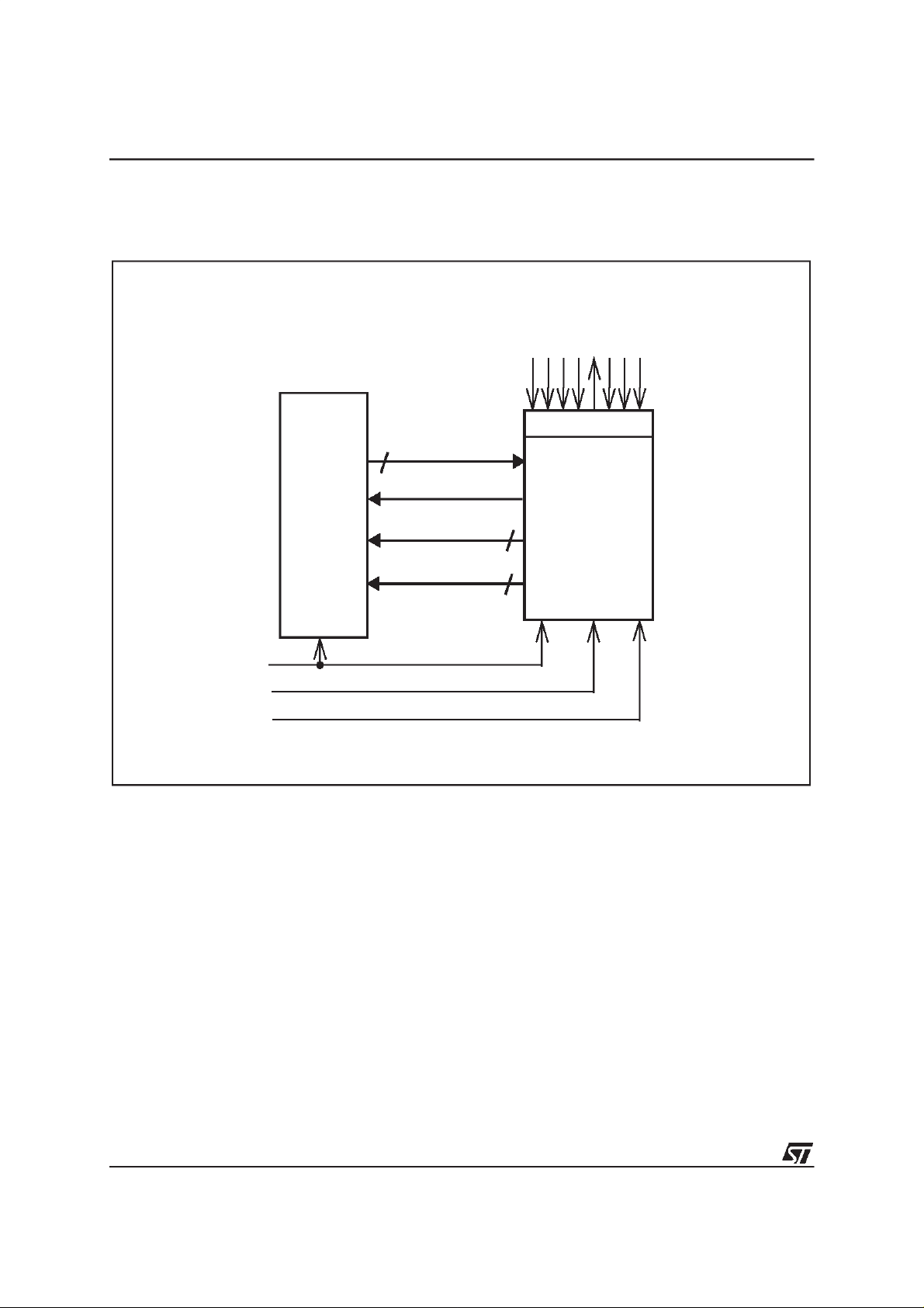
Figure 1.1 FC106 chip connections
1.0625 Gb/s
System 1 System 2
REFCLK (1)
Fibre
Channel
Controller
I/O Bus
10 bits
SerialDataover copper
or optical cables
FC106
REFCLK (2)
FC106
10 bits
Fibre
Channel
Controller
I/O Bus
The parallel interface on the FC106 is compatible with the 10-Bit Interface Specification
(ANSI TR/X3.18-1998) which defines a common, standard signaling interface between the
Fibre Channel Physical and Protocol layers. In addition, the FC106 can be used for all other
proprietary serial links transmitting data as 10-bit encoded characters.
The FC106 incorporates an impedance adaptor circuit (set by the pins ZC+, ZC-) to ensure
high quality adaptation to the transmission line characteristic impedance.This feature is
optional and the user can keep external adaptation for compatibility reasons.
4/32
September 98
Revision 1.2

FC106
The FC106 integrates a loop-back path for system-level test purposes. It also includes a
self-test capability in which random patterns are transmitted through the internal loop-back
path and compared after reception.
The FC106 is implemented in a standard digital 0.35µ CMOS process. Its typical power
consumption is 0.4 Watts (not including the power required to drive the TTL parallel output
port, which is in the 0.1 Watt range for output capacitive loads of 10 pF per pin).
5/32
September 98
Revision 1.2
FC106
2 Interface Diagram
Figure 2.1 Interface diagram
10
TX[0:9]
T
T
T
C
R
M
K
S
S
Test
transmitter
T
D
I
T
DORSA
T
E
T
N
REFCLK
EWRAP
EN_CDET
FC
Protocol
Device
[106.25 MHz]
COM_DET
RBC[0:1]
RX[0:9]
2
10
FC106
receiver
6/32
September 98
Revision 1.2

FC106
3 Functional Description
The FC106 provides all required signals in the 10-Bit Interface Specification for Fibre
Channel. It also provides 10 pins for additional functions (these pins are marked in the
following by *). The additional functions are:
impedance control (ZC+*, ZC-*)
•
• production test through JTAG(TCK
self-test of the chip (AT*)
•
(*)
-TRSTN(*)-TMS(*)-TDI(*)-TDO(*)- TEST ENABLE(*))
• reset pin (RS) (but note that another reset is automatically generated in the chip during
power on).
In addition to implementing the Fibre Channel standard, the FC106 is adaptable through the
JTAGpath to the transmission of any sequence of 10-bit encoded characters at rates varying
between 1 and 1.1 Gbaud.
7/32
September 98
Revision 1.2

FC106
3.1 Block diagram
Figure 3.1 Block diagram
TCK(*)
TRSTN(*)
TMS(*)
TDI(*)
TDO(*)
TEST ENABLE(*)
TX [0:9]
JTAG
CONTROL
ENC
SERIALIZER
XOR
Tree
TX-
transmitter
TX+
8b/10b
encoder
RCB[0:1]
AT (*)
RS (*)
REFCLK
SELF
TEST
ENC
RX[0:9]
3.2 Input latches
8b/10b
decoder
EN_CDET
DLL clock generator
Clock Recovery
Word
Alignment
DESERIALIZER
COM_DET
Bit
Alignment
ZC+(*)
ZC
setting
ZC-(*)
RX-
receiver
RX+
(*)Test signals not
included in FCS
10-bit interface
EWRAP
The transmitter accepts 10-bit wide TTL parallel data at inputs TX[0:9]. The user-provided
reference clock signal REFCLK is also used as the transmit byte clock. The TX[0:9] and
REFCLK signals must be properly aligned, as shown in Section 6.1:
timing and latency
8/32
September 98
on page 20.
Revision 1.2
Transmit interface

FC106
3.3 8bit/10bit Encoder/Decoder
In normal operation mode, the FC106 accepts 10-bit pre-encoded data, and provides to the
application, 10-bit encoded data (as specified in the ANSI 10-bit Interface Specification).
In addition, the FC106 contains an 8b/10b encoder/decoder, which can be inserted into the
data flow. The selection of this mode is made through the JTAG path. In this mode, the
FC106 accepts and delivers bytes on 9 bits (8 bits of data on TX/RX[0:7] and 1 bit on TX/
RX[8] which is used to differentiate control characters). The timings of the parallel I/O ports
are identical in both modes: using the 8b/10b encoder/decoder increases the transmission
latency by 2 byte clock periods (equivalent toa4meterincrease of the cable length).
3.4 DLL clock generator
The DelayLocked Loop (DLL) block generates the internal clocks. These are required by the
transmitter section to perform its function, and by the receiver block to generate the
reference clocks which are used to recover the serial data input frequency. These clocks are
based on the user supplied reference byte clock REFCLK. This clock is multiplied by 10 to
generate the required serial output data rate. No external components are required to
operate the DLL Clock Generator.
3.5 Serializer functional description and reference
clock
The FC106 serializer performs the serialization of 10-bit pre-encoded parallel data at
signaling rates up to 1.0625 Gb/s. System design is simplified by the integration into the chip
of a block performing clock multiplication from the parallel data clock.
It accepts 10-bit encoded parallel data words which are clocked into the device at 1/10 of the
signaling rate. For Fibre Channel use, data should be encoded for transmission using the
8B/10B block code described in the Fibre Channel specification. The FC106 serializes the
input data and transmits it at a signaling rate of 10 times the frequency of the REFCLK input.
The device includes a Delay-Locked-Loop based clock multiplier that generates the
1.0625 Gbaud clocks. This DLL is fully monolithic and requires no external components. Its
acquisition time, at power-up, is less than 16 microseconds.
The FC106 loads parallel data on the rising edge of REFCLK. The delay through the FC106
from loading the code-group to the transmission of the first bit of the code-group on the TX+,
TX- pair, is 17.4 ns with an extra 9.4 ns if the 8b10b encoding function is enabled.
A loop-back-mode signal EWRAP is provided allowing internal dynamic self-test of the chip.
When EWRAP is low, the output of the transmitter is sent to the TX+ and TX- output pins,
and the input of the receiver is driven by the signals entered through the RX+ and RX- pins.
9/32
September 98
Revision 1.2

FC106
When EWRAP is high, the output of the transmitter is sent directly to the input of the
receiver.
3.6 Serializer latches and XOR-tree
The parallel data words TX[0:9] are individually sampled using the clocks provided by the
DLL Clock Generator. The outputs of these serializer latches are merged through an
Exclusive-OR tree, in order to generate the output data bit streams.
3.7 Serial input multiplexer
The Input Multiplexer supports the internal loopback of the high speed serial signal for test
purposes.
In normal operation, EWRAP is set low.The serial output data stream is placed at TX+/TXoutputs, and the serial data accepted at RX+/RX- is transmitted to the deserializer block.
When wrap-mode is activated by setting EWRAP high, the serial data generated by the
serializer block is internally wrapped to the input of the deserializer block.
3.8 Deserializer functional description
The FC106 deserializer operates at signaling rates up to 1.0625 Gb/s, as specified in the
Fibre Channel standard. It extracts the clock and retimes the data from the serial bit stream.
The serial bit stream should be encoded as 10-bit characters (for example the 8B/10B code
for FibreChannel) which provide a transition density greater than 10%. The retimed serial bit
stream is converted into a 10-bit parallel output word. The FC106 has internal DLL based
clock recovery circuit which requires no external components.
When the DLL of the serializer clock multiplier is locked to the expected data rate (defined by
REFCLK), the retiming acquisition time (to lock to the incoming serial data stream) is less
than 3 microseconds.
The FC106 provides byte and data word alignment using a comma symbol recognition
mechanism.
The 7-bit comma symbol is defined in Fibre Channel specification as a [0:6]= 0011111. This
pattern is only contained within special characters known as K28.1, K28.5 and K28.7
defined specifically for synchronization by Fibre Channel.
Serial data is received on the RX+ and RX- pins. The DLL clock recovery circuit will lock to
the data stream if the clock to be recovered is within 0.01% of the expected data rate. For
10/32
September 98
Revision 1.2

FC106
example, if the REFCLK used is 106.25 MHz, then the incoming data serial signaling rate
must be 1.0625 ± 0.0001 Gb/s.
The FC106 provides 2 TTL recovered clocks RBC[0] and RBC[1], which are both driven at a
frequency of one twentieth of the serial signaling rate. These clocks are generated by the
clock recovery DLL, which is phase locked to the serial data. RBC[1] is 180° out of phase
with RBC[0]. If serial data is not present, or does not meet the required transition density or
signaling rate, the RBC frequencies will be half of the expected recovered clock frequency
(defined by REFCLK). This function replaces the optional LCK_REF signal that is specified
in the Fibre Channel 10-bit interface. When no data is present, phase adjustments are
required for switching between a locking to incoming data and locking to REFCLK. The
specification on output clocks RBC[0:1] is maintained during these adjustments.The clock
periods are not truncated.
The serial data is retimed and deserialized. Parallel data is loaded into the output register,
and therefore accessible on the output data port. For Fibre Channel use, bytes 1 and 3 of the
receive data word will be accessible on the rising edge of RBC[0], and bytes 0 and 2 on the
rising edge of RBC[1].
Word synchronization is enabled in the FC106 by connecting the EN_CDET pin to V
When EN_CDET is set high, the FC106 examines serial data for the presence of a positive
disparity comma symbol (0011111). Improper alignment occurs when a comma symbol
straddles a 10-bit boundary or is not aligned within the 10-bit transmission character. Proper
alignment is reached by shifting the boundary of the parallel output.
At power up the FC106 will not be in synchronization and data alignment is not established.
The COM_DET output signal is then set low.When a comma symbol is detected, COM_DET
is set high (if EN_CDET is already set high). COM_DET will go high only during a cycle in
which RBC[1] is rising (see Section 6.2.2:
timing).
Note that if EN_CDET is set low, but a comma is detected while the input stream is already
word-aligned, COM_DET will be set high again.
Receive interface timing
on page 23 for precise
dd
3.9 Bit alignment
The alignment block aligns the incoming data bit stream and the reference clocks generated
by the DLL Clock Generator. It compensates for clock frequency dispersions between the
crystals generating the respective reference clocks REFCLK of the transmitting and
receiving chips.
.
11/32
September 98
Revision 1.2

FC106
3.10 Byte and word alignment
The word alignment function is performed under control of the EN_CDET signal.
When EN_CDET is high, the word alignment function is operational. If an improperly aligned
comma is encountered, the internal data is shifted to realign the comma character at the
deserializer output (RX[0:9]). In this process, up to three characters prior to the comma
character may be corrupted.
3.11 Clock recovery
The clock recovery block generates the two receiver byte clocks RBC[0:1] at half the
frequency corresponding to the RX+/RX- byte data rate. These two byte clocks are 180° out
of phase with each other. They are alternatively used to clock the 10-bit parallel output data.
12/32
September 98
Revision 1.2

FC106
3.12 Serial input-output buffer
Figure 3.2 shows a simplified schematic of the serial I/O.
Figure 3.2 Schematic diagram of serial I/O
V
dd
Dout-
Transmitting Chip
V
dd
Dout+
V
ss
V
ss
RoutTX+ TX-
RsRs
See Section 3.13 for
configuration control
versus line impedance
Receiving Chip
13/32
September 98
1.5 KΩ
1.5 KΩ
0.01µF
RX+
Revision 1.2
Rc
RX-
Rin
TO DESERIALIZER
0.01µF(optional)
1.5 K
1.5 KΩ
Ω

FC106
3.13 I/O impedance control
The ZC block sets the internal RX+/RX- and the TX+/TX- matching impedance. Table3.1
details the different settings.
Table 3.1 ZC block settings
Case 1: 50Ω line
Rs = 0Ω
Rout= 100Ω
Rs = 0Ω
Case 2: 50Ω line
Rs = 0Ω
Rout= 100Ω
Rs = 0Ω
Case 3: 75Ω line
Rs = 25Ω
Rout= 100Ω
Rs = 25Ω
Ω
Rin = 100
Ω
Rc = 150
Ω
Rc = 100
ZC+ ZC-
LINE = 50Ω
Ω
R > 1.5K
receivertransmitter
External Rc
LINE = 50Ω
Ω
No external Rc
OPEN
or V
dd
V
ss
OPEN
or V
OPEN
or V
ADD Rs
+/-1%
0 Ω 100 Ω
dd
0 Ω NONE
dd
ADD Rc
+/-1%
Use internal Rc
R>1.5K
receivertransmitter
LINE = 75Ω
Ω
R>1.5K
receivertransmitter-
External Rc
OPEN
or V
dd
OPEN
or V
dd
25 Ω 150 Ω
Case 4: 75Ω line
LINE = 75Ω
Rs = 0Ω
Rout= 150Ω
Rs = 0Ω
Ω
Rc = 150
Ω
R>1.5K
receivertransmitter
External Rc
OPEN
or V
dd
V
0 Ω 150 Ω
ss
Case 5: 75Ω line
Rs = 0
LINE = 75Ω
Ω
Ω
Ω
No external Rc
V
V
ss
0 Ω NONE
ss
Use internal Rc
Rout = 150Ω
Rs = 0Ω
Rin =150
R>1.5K
receivertransmitter
Case 3 and 4 are identical applications: Case 3 allows better on board compatibility with other
FC parts that request 25Ω series resistors. Exact value of R
5.3:
DC characteristics
on page 18.
and Rinare detailed in Section
out
14/32
September 98
Revision 1.2

FC106
3.14 Self-test
The self-test block generates its own internal clock (the frequency of which can be digitally
tuned through the JTAG port), and pseudo-random patterns. This data is encoded,
serialized, deserialized (through the loop-back test path, or through an external connection
between TX+/TX- and RX+/RX-) and decoded. The recovered data is checked; the errors
and the number of transmitted bytes are internally counted. The contents of these counters
are accessible through the JTAG path. This block is activated by the AT signal.
In normal operation, AT is tied to V
During production tests, AT is forced to V
level.
and the self-test block is disabled.
dd
, allowing full speed dynamic tests, even at wafer
ss
15/32
September 98
Revision 1.2

FC106
4 Serial I/O Electrical Model
This simplified model is given for typical board simulation, within 15% precision. The
termination at the receiving end can be either internal or external, following Section 3.13.
Figure 4.1 Serial I/O electrical schematic diagram
V
ss
Tr
0.01µF(optional)
V
dd
R1
Zc = 40
Ω
Td = 0.15nS
Ω
Zc = 60
Td = 0.15nS
Tr = Tf = 0.2nS
1pF
Rout
Rc
1pF
V
dd
Tf
R1
Zc = 40
Ω
Td = 0.15nS
0.01µF(optional)
Zc = 60
Ω
Td = 0.15nS
V
ss
Simplified serial
transmitter model
Simplified QFP64
package model
Your board and/or
cable/connector model
Simplified QFP64
package model
PARAMETER VALUES
FOR TYPICAL
SIMULATION
16/32
September 98
0.5pF0.5pF
Simplified serial
Rin
receiver model
1.5K
Ω 1.5KΩ
50ΩCONFIGURATI ON 75ΩCONFIGURATION
R1 100Ω 150Ω
Rout 200Ω 300Ω
Rc 100Ω if external termination 150Ω if external termination
Rin 100Ω if internal termination 150Ω if internal termination
Ω
1.5K
TO DESERIALIZER
1.5KΩ
Revision 1.2

FC106
5 Electrical Specifications
5.1 Absolute maximum ratings
Table 5.1 Absolute maximum ratings
Symbol Parameter Units Min Max
V
dd
V
INL
V
INH
T°C
MAX
Supply Voltage V 0 4
Serial signal input low level V -0.5
Serial signal input high level
ZC+, ZC-
TTL input signals
Maximum assembly temperature (for
10 seconds maximum)
Storage temperature
V
V
V
°C
°C -65
Vdd+0.5
Vdd+0.5
5.5
260
150
Note Stresses greater those listed under “Absolute Maximum Ratings” may cause
permanent damage to the device. This is a stress rating only and functional
operation of the device at these or any other conditions above those indicated in the
operational sections of this specification is not guaranteed. Exposure to absolute
maximum rating conditions for extended periods may affect device reliability. During
overload conditions (
(
V
) must not exceed the values defined by the Absolute Maximum Ratings.
ss
V
IN>Vdd
or
V
<
V
IN
) the voltage on pins with respect to ground
ss
5.2 Operating conditions
Table 5.2 Operating conditions
Symbol Parameter Units Min Typ Max
V
dd
T
A
IDD Supply current @ 25°C, 3.3 volts
17/32
September 98
Supply Voltage V 3.0 3.3 3.6
Supply Ripple (DC to 3 GHz) mV 100
Ambient temperature °C02570
mA 150
with parallel outputs loaded by 10pF
Revision 1.2

FC106
5.3 DC characteristics
The following values apply to the analog signals TX+, TX-, RX+ and RX-
Table 5.3 DC characteristics for TX+, TX-, RX+ and RX-
Symbol Parameter Units Min. Typ Max.
V
OLS50
V
OHS50
V
OLS75
V
OHS75
V
OD50
V
OD75
R
OUT50
R
OUT75
R
IN50
R
IN75
V
ISWS
Serial output low level, terminated differentially by an external 100Ω resistor
( Zc+ = Zc- = “open” )
Serial output high level, terminated differentially by an external 100Ω resistor
( Zc+ = Zc- = “open” )
Serial output low level, terminated differentially by an external 150Ω resistor
( Zc+ = “open” - Zc- = “Vss” )
Serial output high level, terminated differentially by an external 150Ω resistor
( Zc+ = “open” - Zc- = “Vss” )
Serial output peak-to-peak differential voltage, terminated differentially by an external
100Ω resistor ( Zc+ = Zc- = “open” )
Serial output peak-to-peak differential volt-
age, terminated differentially by an external
150Ω resistor ( Zc+ =”open” - Zc- = “Vss” )
Internal differential output impedance. When
50Ω line ( Zc+ = Zc- = “open” )
Internal differential output impedance. When
75Ω line ( Zc+ =”open” - Zc- = “Vss” )
Internal differential input impedance. When
enabled for 50Ω line ( Zc+ = Vss / Zc- =
“open” )
Internal differential output impedance. When
enabled for 75Ω line ( Zc+ = Zc- = Vss )
Serial input peak-to-peak differential voltage
on RX+ and RX-
V 0.90 1.05 1.20
V 1.50 1.80 2.10
V 0.90 1.05 1.20
V 1.50 1.80 2.10
V 1.20 1.50 1.80
V 1.20 1.50 1.80
Ω 77 100 169
Ω 116 150 255
Ω 59 100 183
Ω 95 150 265
V0.2--
Note Values above are given with normal Zc setting. In accordance with Section 3.13, it
is still possible to stay with 50
Ω
internal control and connect the part to 75
Ω
impedance line by adding 25Ωseries resistances.
18/32
September 98
Revision 1.2

FC106
The following values apply to the logic signals.
Table 5.4 DC characteristics for logic signals
Symbol Parameter Conditions Units Min. Typ Max
V
IL
V
IH
VOL Low level output voltage Vdd=3.3V
VOH High level output voltage Vdd=3.3V
I
IL
I
IH
Input “low” voltage level Vdd=3.3V V - - 0.8
Input “high” voltage level Vdd=3.3V V 2.0 - 5.5
Iol = 3mA
Ioh = 3mA
Input low current Vdd=max
Vin=GND
Input high current Vdd=max
Vin=V
dd
V0.4
V2.4
µA 125
µA 125
19/32
September 98
Revision 1.2

FC106
6 Timing Specifications
All AC measurements are made from the reference voltage level of the clock (1.4 volts), to
the valid input or output data levels.
6.1 Transmit interface timing and latency
Figure 6.1 Transmit interface timing and latency
REFCLK
T
ref
TX[0:9]
VALID
DATA 1
Tsu_tx
VALID
DATA 2
Th_tx
VALID
DATA 3
bit 0 of parallel input (TX0of DATA 1)
TX+
T
ELA
Table 6.1 Transmit interface timing characteristics
Parameter Description Min Typ Max Units
F
=1/T
ref
F
tol
T
r
T
f
CLKJIT REFCLK Jitter 40 pS
DT REFCLK duty Cycle 40 - 60 %
Tsu_tx Data set-up to a rising edge of REFCLK 0 - - ns
Th_tx Data hold after a rising edge of REFCLK 1.5 - - ns
TX-Tr,Tf Parallel data rise and fall time (10 pF load) 0.6 - 3 ns
T
ELA
Reference clock frequency 100 106.25 110 MHz
ref
Frequency tolerance (dispersion between
REFCLK of transmitter and receiver chips)
REFCLK Clock Rise Time (0.8 to 2V) 0.6 - 2.4 nS
REFCLK Clock Fall Time (0.8 to 2V) 0.6 - 2.4 nS
Data Emission Latency (delay from the initial
10-bit word load to the serial transmission of bit 0)
100 - + 100 ppm
- - 1 REFCLK
cycle + 8 ns
1.4V
2.0V
1.4V
0.8V
20/32
September 98
Revision 1.2

FC106
6.2 Receive interface timing
6.2.1 Receive clock timing and latency
Figure 6.2 Receive clock timing
bit 0 of serial
data
TX+
Trbc1
RBC[1]
Trbc_skew
RBC[0]
Trbc0
1.4V
1.4V
Table 6.2 Receive clock timing characteristics
Parameter Description Min Typ Max Units
Trbc0
Trbc1
Trbc_skew RBC skew 8.9 - 9.9 ns
RBC[0,1] Tr, Tf Receive clock rise and fall time
1. Exact frequency of RBC(0,1) depends upon thereceived data frequency. During byte alignment, the frequency of clocks RBC[0]and RBC[1] mayvary by less than 1% of the specified
typical value. The clocks are guaranteed to be glitch free.
RBC[0] frequency
RBC[1] frequency
(10pF load)
1
1
- 2.5 - ns
53.125 MHz
53.125 MHz
21/32
September 98
Revision 1.2

FC106
Figure 6.3 Receive clock latency
bit 0 of serial
data 1
TX+
RBC[1]
RBC[0]
RX[0:9]
T
RLA
DATA 1
Table 6.3 Receive clock latency characteristics
Parameter Description Min Typ Max Units
T
RLA
Data Reception Latency: Serial (first bit at
receiver) to 10-bit parallel output sampled by
RBC[0,1].
--5RBC
cycles
+4ns
ns
22/32
September 98
Revision 1.2

FC106
6.2.2 Receive interface timing
Figure 6.4 Receive interface timing
RBC[0]
RBC[1]
RX[0:9]
COM_DET
Tsu_rx1
Tsu_com
Th_rx1
COMMA
CHARACTER
Tsu_rx0
Th_com
VALID
DATA
Th_rx0
1.4V
1.4V
2.0V
0.8V
2.0V
0.8V
Table 6.4 Receive interface characteristics
Parameter Description Min Typ Max Units
Tsu_rx1 Data valid before a rising edge of RBC[1] 3 - - ns
Th_rx1 Data valid after a rising edge of RBC[1] 1.5 - - ns
Tsu_rx0 Data valid before a rising edge of RBC[0] 3 - - ns
Th_rx0 Data valid after a rising edge of RBC[0] 1.5 - - ns
Tsu_com Signal COM_DET valid before a rising edge of
RBC[1]
23/32
September 98
Revision 1.2
3--ns

FC106
Parameter Description Min Typ Max Units
Th_com Signal COM_DET valid after a rising edge of
RBC[1]
COM_DET Tr, Tf COM_DET rise and fall time (10pF load) 2.5 ns
RX[0:9] RX(n) rise and fall time (10pF load) 2.5 ns
1.5 - - ns
6.3 Serial Input/output AC characteristics
Table 6.5 Serial I/O AC characteristics
Parameter Description Min Typ Max Units
t
RS
t
FS
t
SK
Serial output rise time, terminated by the FC106
receiver (20%-80%)
Serial output fall time, terminated by the FC106
receiver (20%-80%)
Differential skew between TX+ and TX-,
terminated by the FC106 receiver
-200- ps
-200- ps
--25ps
24/32
September 98
Revision 1.2

FC106
7 FC106 Pin Description
7.1 Pin summary
Table 7.1 Pin summary
Pin Level Description
AT* CMOS This signal places the chip in a self-test mode when tied low. It should be
tied to Vddin any other state of the chip, as specified in the 10-Bit Interface
Specification standard.
COM_DET CMOS COM_DET is an indication that the data byte (byte 0 of word 0) associated
with the current RBC[1] contains a valid comma symbol.
EN_CDET CMOS EN_CDET enables the chip to perform the byte alignment function on
comma symbols. When EN_CDET is high, the byte alignment function is
operational.
When EN_CDET is low, the current byte alignment is maintained.
EWRAP CMOS EWRAP causes the chip to internally loop serialized transmit data to the
deserializer. EWRAP is active on high level.
RBC[0] CMOS RBC[0] is the 53.125 MHz receive byte clock that the protocol device will
use to register the bytes 1 and 3 of the received data word. This clock may
be stretched during byte alignment (never slivered or truncated).
RBC[1] CMOS RBC[1] is the 53.125 MHz receive byte clock that the protocol device will
use to register the bytes 0 and 2 of the received data word. RBC[1] is 180°
out of phase with RBC[0]. This clock may be stretched during byte alignment (never slivered or truncated).
REFCLK CMOS REFCLK is the 106.25 MHz reference clock. The frequency tolerance for
this clock should meet ANSI X3.230-1994 Fibre Channel FC-PH specifications for a Fibre Channel use. See Section 6.1:
and latency
RX+, RX- Special RX+ and RX- are the differential inputs for serialized data on the receiver.
RX[0:9] CMOS RX[0:9] is the 10-bit parallel received data presented by the chip to the
upper layer forfurther processing. The received data byte 0 containing the
comma symbol will be byte aligned to RBC[1], i.e. byte 0 is in phase with
RBC[1]. The order of reception on the serial input is RX[0] first, followed by
RX[1] through to RX[9].
TCK*,
TRSTN*,
TMS*, TDI*,
TDO*
TEST
ENABLE*
TX+, TX- Special TX+ and TX- are the differential outputs for serialized data on the
CMOS These signals are compliant to the JTAG specification.
CMOS Used during ATPG test, connected at Vssin normal operation.
transmitter.
on page 20.
Transmit interface timing
25/32
September 98
Revision 1.2

FC106
Pin Level Description
TX[0:9] CMOS TX[0:9] is the 10-bit parallel transmit data presented to the chip for serial-
ization and transmission onto the media. The order of transmission is TX[0]
through to TX[9].
ZC+1,ZC-*
1. indicates signals that are not included in the Fibre Channel 10-Bit Interface Specification.
CMOS These pins are used to control the input and output impedance in accor-
dance with the configuration outlined in Section 3.13:
trol
on page 14.
I/O impedance con-
7.2 Pin functions
Table 7.2 Pin functions
Pin Name Pin # I/O
V
ss
TX[0] 2 I pd Bit 0 of parallel transmit data (first bit sent)
TX[1] 3 I pd Bit 1 of parallel transmit data
TX[2] 4 I pd Bit 2 of parallel transmit data
V
dd
TX[3] 6 I pd Bit 3 of parallel transmit data
TX[4] 7 I pd Bit 4 of parallel transmit data
TX[5] 8 I pd Bit 5 of parallel transmit data
TX[6] 9 I pd Bit 6 of parallel transmit data
V
dd
TX[7] 11 I pd Bit 7 of parallel transmit data
TX[8] 12 I pd Bit 8 of parallel transmit data
TX[9] 13 I pd Bit 9 of parallel transmit data (last bit sent)
V
ss
Vss/RS 15 (I) pd Must be tied to GND during normal operation.
NC/TDI 16 (I) pd Not connected JTAG
NC/TCK 17 (I) pd Not connected Test clock
1 - - Ground Pin
5 - - PowerPin
10 - - PowerPin
14 - - Ground Pin
pull up/
down
Description in standard running conditions
During power up, an internal circuit will
automatically reset the chip. Nevertheless RS
allows a forced reset (when high), during normal
operation.
TEST
pins
External
reset
scan in
pin for
JTAG
26/32
September 98
Revision 1.2

FC106
Pin Name Pin # I/O
pull up/
down
Description in standard running conditions
TEST
pins
Vdd/TRSTN 18 (I) pu Must be tied to Vdd. Reset pin
for JTAG
EWRAP 19 I pd When tied to Vdd, causes the chip to internally
loop serialized transmit data to the deserializer.
Vdd/TMS 20 (I) pu Must be tied to Vdd. Test mode
select for
JTAG
V
ss
21 - - Ground Pin
REFCLK 22 I pd Reference clock frequency 106.25 MHz
V
dd
23 I - Power Pin
EN_CDET 24 I pu Enables the chip to perform the byte alignment
function when HIGH.
TEST
ENABLE
25 I pd Must be tied to GND. Tie to V
for AT PG
dd
NC/TDO 26 (O) - Not connected JTAGscan
out
NC 27 - - Not connected
Vdd/AT 28 (I) pu Must be tied to Vdd. Places the
chip in
auto test
mode
when
LOW.
V
dd
29 - Power Pin
RBC[1] 30 O - Receive byte clock used by the protocol to
register byte 0 and 2 of the receive parallel data.
RBC[0] 31 O - Receive byte clock used by the protocol to
register byte 1 and 3 of the receive parallel data.
V
ss
V
ss
32 - - Ground Pin
33 - - Ground Pin
RX[9] 34 O - Bit 9 of parallel receive data (last bit received)
RX[8] 35 O - Bit 8 of parallel receive data
RX[7] 36 O - Bit 7 of parallel receive data
V
dd
37 - - Power Pin
RX[6] 38 O - Bit 6 of parallel receive data
RX[5] 39 O - Bit 5 of parallel receive data
RX[4] 40 O - Bit 4 of parallel receive data
RX[3] 41 O - Bit 3 of parallel receive data
V
dd
42 - - Power Pin
27/32
September 98
Revision 1.2

FC106
Pin Name Pin # I/O
pull up/
down
Description in standard running conditions
RX[2] 43 O - Bit 2 of parallel receive data
RX[1] 44 O - Bit 1 of parallel receive data
RX[0] 45 O - Bit 0 of parallel receive data (first bit received).
V
ss
46 - - Ground Pin
COM_DET 47 O - Goes high when detecting a comma symbol.
Data byte associated with RBC[1] contains valid
comma symbol.
ZC- 48 1 pu Used for impedance adaptation (see
Section 3.13)
ZC+ 49 1 pu Used for impedance adaptation (see
Section 3.13)
V
dd
V
ss
50 - - Power Pin
51 - - Ground Pin
RX- 52 I - One of the differential inputs for serialized data
on the receiver. Serial input frequency must be
1.0625 ± 0.0001 Gb/s.
V
dd
53 - - Power Pin
RX+ 54 I - One of the differential inputs for serialized data
on the receiver. Serial input frequency must be
1.0625 ± 0.0001 Gb/s.
V
dd
V
ss
V
dd
V
ss
V
dd
V
dd
55 - - Power Pin
56 - - Ground Pin
57 - - Power Pin
58 - - Ground Pin
59 - - Power Pin
60 - - Power Pin
TX- 61 O - One of the differential outputs for serialized data
on the transmitter. Serial output rate depends on
REFCLK.
TX+ 62 O - One of the differential outputs for serialized data
on the transmitter. Serial output rate depends on
REFCLK.
V
dd
63 - - Power Pin
NC 64 - - Not connected
TEST
pins
28/32
September 98
Revision 1.2

FC106
8 Package Specifications
The FC106 is available in two sizes of 64-pin plastic quad flat-pack: the FC106/14 measures
14x14 mm and the FC106/10 measures 10x10 mm.
8.1 FC106 64-pin PQFP pinout
Figure 8.1 Pinout for 64-pin PQFP (both 14x14 mm and 10x10 mm sizes)
Vdd
Vss
TX0
TX1
TX2
Vdd
TX3
TX4
TX5
TX6
Vdd
TX7
TX8
TX9
Vss
Vss
NC
NC
64 62 61 60 59 58 57 56 5563 54 53 52 51 50 49
1
2
3
4
5
6
7
8
9
10
11
12
13
14
15
RS (test mode)
16
TDI
TCK
17 19 20 21 22 23 24 25 2618 27 28 29 30 31 32
TX+
TX-
Vdd
Vdd
Vdd
Vss
Vdd
Vss
FC 106
JTAG PINS
TRSTN
TMS
TEST
TDO
ENABLE
Vdd
RX+
RX-
AT(for testingpurposes)
Vdd
Vss
ZC+
48
47
46
45
44
43
42
41
40
39
38
37
36
35
34
33
ZCCOM_DET
Vss
RX0
RX1
RX2
Vdd
RX3
RX4
RX5
RX6
Vdd
RX7
RX8
RX9
Vss
29/32
September 98
NC
Vdd
NC+
Vss
Vdd
EWRAP
Vdd
REFCLK
Vss
EN_CDET
NC
Vdd
Vdd
RBC[1]
Vss
RBC[0]
Revision 1.2

FC106
8.2 FC106 64-pin Quad Flat-pack package dimensions
8.2.1 FC106/14: 14x14 mm package dimensions
Figure 8.2 Data for 64-pin 14x14 mm PQFP
mm inch
DIM
MIN. TYP. MAX. MIN. TYP. MAX.
A - - 2.35 - - 0.093
A1 - 0.25 - - 0.010
A2 1.95 2.00 2.10 0.077 0.079 0.083
b 0.30 0.35 0.40 0.012 0.014 0.016
c - - 0.17 - - 0.067
D 16.95 17.20 17.45 0.667 0.677 0.687
D1 13.90 14.00 14.10 0.547 0.551 0.555
D2 - 12.00 - - 0.472 e - 0.80 - - 0.031 E 16.95 17.20 17.45 0.667 0.677 0.687
E1 13.90 14.00 14.10 0.547 0.550 0.555
E2 - 12.00 - - 0.472 -
θ
0°-7°
L 0.78 0.88 1.03 0.031 0.035 0.041
D
D
D1
D1
D2
PQFP64
Body: 14 x 14 x 2.0 mm
Footprint: 3.20 mm
Thermal resistance = 45°C/W (still air)
A
A
A2
A2
A1
A1
48
49
49
b
B
64
64
1
1
30/32
September 98
3348
33
32
32
E2 E1 E
E3D3E1
17
17
16
16
e
e
PQFP64
PQFP64
E
L1
L
L
Seating Plane
SeatingPlane
θ
K
0.10mm
0.1mm
b
B
c
C
Revision 1.2

FC106
8.2.2 FC106/10: 10x10 mm package dimensions
Figure 8.3 Data for 64-pin 10x10 mm PQFP
mm inch
DIM
MIN. TYP. MAX. MIN. TYP. MAX.
A - - 2.45 - - 0.097
A1 0.25 - 0.50 0.010 - 0.020
A2 1.95 2.00 2.10 0.077 0.079 0.083
b 0.17 0.22 0.27 0.007 0.009 0.011
c - - 0.17 - - 0.067
D 12.95 13.20 13.45 0.510 0.520 0.530
D1 9.90 10.00 10.10 0.390 0.394 0.398
D2 - 7.50 - - 0.295 e - 0.50 - - 0.020 E 12.95 13.20 13.45 0.510 0.520 0.530
E1 9.90 10.00 10.10 0.390 0.394 0.398
E2 - 7.50 - - 0.295 -
θ
0°-7°
L 0.78 0.88 1.03 0.031 0.035 0.041
D
D
D1
D1
D2
PQFP64
Body: 10 x 10 x 2.0 mm
Footprint: 3.20mm
Thermal resistance = 45°C/W (still air)
A
A
A2
A2
A1
A1
48
49
49
b
B
64
64
1
1
31/32
September 98
3348
33
32
32
E2 E1 E
E3D3E1
17
17
16
16
e
e
PQFP64
PQFP64
E
L1
L
L
Seating Plane
SeatingPlane
θ
K
0.10mm
0.1mm
b
B
c
C
Revision 1.2

FC106
Information furnished is belived to be accurate and reliable. However, STMicroelectronics assumes no responsibility
for the consequences of use of such information nor for any infringement of patents or other rights of thirdparties which
may result from its use. No license is granted by implication or otherwise under any patent or patent rights of
STMicroelectronics. Specifications mentioned in this publication are subject to change without notice. This publication
supersedes and replaces all information previously supplied. STMicroelectronics products are not authorized for use
as critical components in life support devices or systems without express written approval of STMicroelectronics. This
circuit uses patents licensed by BULL S.A..
The ST logo is a trademark of STMicroelectronics.
1998 STMicroelectronics - All Rights Reserved
STMicroelectronics GROUP OF COMPANIES
Australia - Brazil - Canada - China - France - Germany - Italy - Japan - Korea - Malaysia - Malta - Mexico - Morocco -
The Netherlands - Singapore - Spain - Sweden - Switzerland - Taiwan - United Kingdom - U.S.A.
32/32 Document Number 42 1686
September 98
Revision 1.2
32
 Loading...