

QUAD COMPARATOR INTERFACECIRCUIT
.
MINIMUM HYSTERESIS VOLTAGE AT EACH
INPUT: 0.3V
.OUTPUTCURRENT : 15 mA
.LARGESUPPLY VOLTAGERANGE: + 10Vto
+35V
.
INTERNAL THERMALPROTECTION
.INPUT AND OUTPUT CLAMPING PROTEC-
TIONDIODES.
DESCRIP TION
TheESM1602Bisa quadruplecomparatorintented
to provide an interface between signal processing
and transmitting lines in very noisy industrial surroundings.
Outputof eachcomparator,usedaslinedriver,suppliesa constantcurrent (PNP output stage)and is
specially well protected against powerful overvoltages.The open collector output circuit allows the
connectionofseveralcomparatorsto asingletransmitting line.
The ESM1602Bcan operate as receiver on a line
transmitting noisy high-voltagesignals. Hysteresis
effect, internally implemented on inputs of each
comparator providesan excellentnoise immunity.
In addition, each input is also protected against
overvoltages.
ESM1602B
DIP14
SO16
ORDER ING NUMBERS: ESM1602B (DIP14)
The ESM1602Bcan operate in a wide supply voltage range (standard operational amplifier ±
supplyor single + 12 V or + 24 V suppliesusedin
industrialelectronicsets).
Moreover,internalthermal protection circuitry cuts
outtheoutputcurrentofthefourcomparatorswhen
powerdissipationbecomesexcessive.
ESM1602BFP(SO16)
15 V
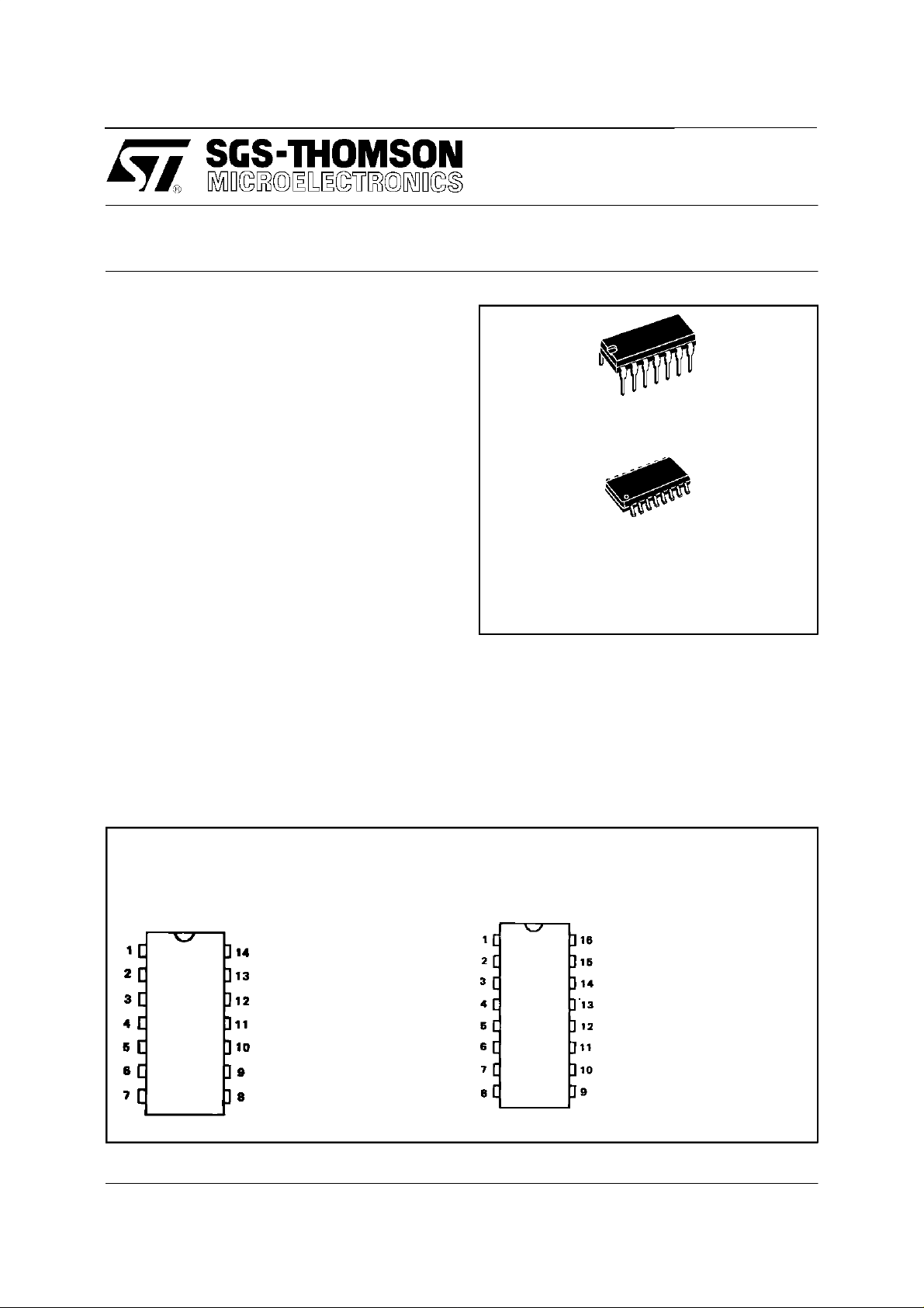
PIN CONNECTIO NS (top view)
DIP14 SO16
1 -Inverting input 1
2 -Non-inverting input 1
3 -Output 1
4 -Non-inverting input 2
5 -Inverting input 2
6 -Output 2
7 -GND
8 -Output 3
9 -Inverting input 3
10 -Non-inverting input 3
11 -Output 4
12 -Non-inverting input 4
13 -Inverting input 4
14 -V
CC
January1996
1 -Inverting input 1
2 -Non-inverting input 1
3 -Output 1
4 -Non-inverting input 2
5 -Inverting input 2
6 -Output 2
7 -GND
8 -N.C.
9 -N.C.
10-Output 3
11-Inverting input 3
12-Non-inverting input 3
13-Output 4
14-Non-inverting input 4
15-Inverting input 4
16-V
CC
1/11

ESM1602B
SCHEMATIC DIAGRAM
ABSOLUTE MAXIMUM RATINGS
Symbol Parameter Value Unit
V
V
V
I
O (max)
P
T
T
Supply Voltage 45 V
CC
Differential Input Voltage 45 V
ID
Input Voltage –0.7 to +45 V
I
Output Current Internally Limited mA
Power Dissipation Internally Limited W
tot
Operating Ambient Temperature Range –25 to +85
op
Storage Temperature Range –40 to +150
stg
o
C
o
C
2/11

ESM1602B
ELECTRICAL CHARACTERISTICS
=
V
+35V, -25
CC
Symbol Parameter Min. Typ. Max. Typ. Fig.
+
V
I
–
V
I
V
C
I
IB
I
SC
V
CC–VO
V
O
I
CC
S
VO
V
F
– Energy of Pulses against which Circuit Output is Protected
– Pulsed Current Applied to Protective Output Diodes
Notes : 1. When negative inputis biased between0 and 2 volts output is always low.
2. Comparator hysteresis voltageon positiveinput on the one handand negativeinput on the other hand equalssumofinputcontrol
voltages V
3. Inputcurrent flows out of thecircuitowing toPNP inputstage. This current isconstant and independent ofoutputlevel.Sonoload
changeis transmittedtoinputs.
4. By definition,a circuit is immunized againstpowerful signals when no durable characteristic change occurs aftertheapplication of
thesesignals and when the circuithas not been destroyed.
In industrialsurroundings, parasitic signals containusually highvoltage (over 200 V) AC harmonics having variable impedance of
500 Ω to10kΩ.
Thepowerdissipationofthesesignalsis dividedbetweenclampingdiodesandtheV
energy level.The injectedcurrent valuecannotin any caseexceed3A.
5. Output protectivediodes are testedindividually by means of positiveand negative discharge voltagesofa capacitor. Thenegative
discharge controloccurs througha singlediode.Duringpositivedischarge, due totheproperties of integration,a groundedcollector
PNP transistorappearsin parallelwiththe clamping diodeconnected to V
beinggreater than VCC. If T is the totaldischarge duration, energy dissipated in the circuitis:
o
C ≤ T
≤ +85oC (unless otherwise specified)
amb
Input Voltage Range - Note 1
Non-inverting Input
Inverting Input
0
2
33
33
V
V
Input Control Voltage (2V < VCM< 33V) - Note 2 150 500 mV 8
Input Bias Current - Note 3 1 5
µA
Short-circuit Output Current
= +10 to +35 V 6 25 mA
V
CC
Output Saturation Voltage (high level) - (IO= –10mA) 1 1.5 V 11
Output Saturation Voltage (high level) - (IO= –10mA) 1 1.6 V 12
Supply Current
R
=∞for the 4 Comparators
L
Common for the 4 Comparators
R
L
Output Slew-rate (RL=3kΩ,T
amb
= +25oC)
4
10
1
13
6
mA
mA
V/µs
Input Protective Diode Forward Voltage
(I = 20mA, T
= +25oC) - Note 4 20 mJ
(T
amb
= +25oC) - Note 5 0.4 A 15
(T
amb
C1+VC2
= +25oC) 1.5 V
amb
orVC3+V
C4.
.Simulationisusedtodeterminethemaximum
CC
. A partofthe current flowsthrough this transistor, V
CC
9
13,14
CE
Fora certaininjected current, the lower thecurrent I
cuit.Topology andtechnological processeshave been chosen to shortenthis current gain.
, thatistosaythelower the PNP currentgain the smaller theenergy is dissipatedinthecir-
2
W=
T
[i
1⋅vd +i2 (VCC + vd)
⌠⌡
O
]
dt
3/11

ESM1602B
Figure 1: InputBias Current Figure2: OutputSaturationVoltage
Figure 3:
OutputSaturationVoltage
Figure4:
ShortCircuit Current
4/11

TYPICAL APP L ICATIONS
Figure 5 :Conversionof DTL, TTL, MOSSignalson a TransmittingLine.
ESM1602B
Figure6 :
Receptionof HighlyNoisySignals.
5/11

ESM1602B
Figure 7.
TEST CIRCUITS
Figure 8.
6/11

Figure 9. Figure 10.
Figure 11. Figure12.
ESM1602B
Figure 13. Figure14.
7/11

ESM1602B
Figure 15.
Figure 16:
ResponseTime.
8/11

DIP14PACKAGEMECHANICAL DATA
Dimensions Millimeters Inches
Min. Typ. Max. Min. Typ. Max.
a1 0.51 0.020
B 1.39 1.65 0.055 0.065
b 0.5 0.020
b1 0.25 0.010
D 20 0.787
E 8.5 0.335
e 2.54 0.100
e3 15.24 0.600
F 7.1 0.280
i 5.1 0.201
L 3.3 0.130
Z 1.27 2.54 0.050 0.100
ESM1602B
DIP14.TBL
9/11

ESM1602B
S016PACKAGE MECHANICAL DATA
Dimensions Millimeters Inches
Min. Typ. Max. Min. Typ. Max.
A 1.75 0.069
a1 0.1 0.2 0.004 0.008
a2 1.6 0.063
b 0.35 0.46 0.014 0.018
b1 0.19 0.25 0.007 0.010
C 0.5 0.020
c1 45
D 9.8 10 0.386 0.394
E 5.8 6.2 0.228 0.244
e 1.27 0.050
e3 8.89 0.350
F 3.8 4.0 0.150 0.157
G 4.6 5.3 0.181 0.209
L 0.5 1.27 0.020 0.050
M 0.62 0.024
S8
o
(typ.)
o
(max.)
SO16.TBL
10/11

ESM1602B
Information furnished is believed to be accurate and reliable. However, SGS-THOMSON Microelectronics assumes no responsibility for
the consequences of use of such information nor for any infringement of patents or other rights of third parties which may result from its
use. No license is granted by implication or otherwise under any patent or patent rights of SGS-THOMSON Microelectronics. Specification
mentioned in this publication are subject to change without notice. This publication supersedes and replaces all information previously
supplied. SGS-THOMSON Microelectronics products are not authorized for use as critical components in life support devices or systems
without express written approval of SGS-THOMSON Microelectronics.
Australia - Brazil - Canada - China - France - Germany - Hong Kong - Italy - Japan - Korea - Malaysia - Malta - Morocco -
The Netherlands - Singapore - Spain - Sweden - Switzerland - Taiwan - Thailand - United Kingdom - U.S.A.
1997 SGS-THOMSON Microelectronics – Printedin Italy – All Rights Reserved
SGS-THOMSON Microelectronics GROUP OF COMPANIES
11/11
 Loading...