

SGS Thomson Microelectronics ESM1600BFP, ESM1600B Datasheet
QUAD COMPARATOR INTERFACECIRCUIT
.
MINIMUM HYSTERESIS VOLTAGE AT EACH
INPUT: 0.3V
.OUTPUTCURRENT : 15 mA
.LARGESUPPLY VOLTAGERANGE: + 10Vto
+35V
.
INTERNAL THERMALPROTECTION
.INPUT AND OUTPUT CLAMPING PROTEC-
TIONDIODES.
DESCRIP TION
TheESM1600Bisa quadruplecomparatorintented
to provide an interface between signal processing
and transmitting lines in very noisy industrial surroundings.
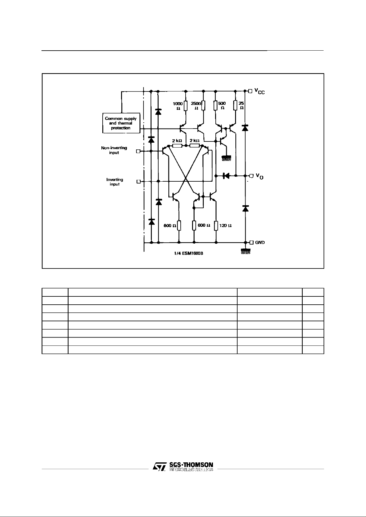
Outputof eachcomparator,usedaslinedriver,suppliesa constantcurrent (PNP output stage)and is
specially well protected against powerful overvoltages.The open collector output circuit allows the
connectionofseveralcomparatorsto asingletransmitting line.
The ESM1600Bcan operate as receiver on a line
transmitting noisy high-voltagesignals. Hysteresis
effect, internally implemented on inputs of each
comparator providesan excellentnoise immunity.
In addition, each input is also protected against
overvoltages.
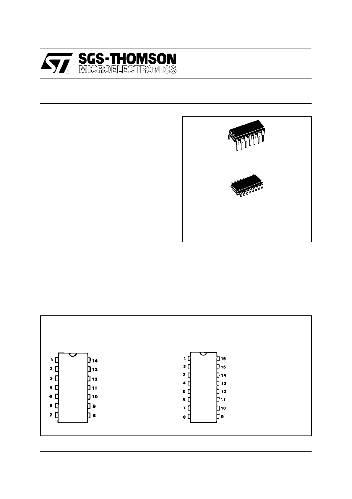
ESM1600B
DIP14
SO16
ORDER ING NUMBERS: ESM1600B (DIP14)
The ESM1600Bcan operate in a wide supply voltage range (standard operational amplifier ±
supplyor single + 12 V or + 24 V suppliesusedin
industrialelectronicsets).
Moreover,internalthermal protection circuitry cuts
outtheoutputcurrentofthefourcomparatorswhen
powerdissipationbecomesexcessive.
ESM1600BFP(SO16)
15 V
PIN CONNECTIO NS (top view)
DIP14 SO16
1 -Inverting input 1
2 -Non-inverting input 1
3 -Output 1
4 -Non-inverting input 2
5 -Inverting input 2
6 -Output 2
7 -GND
8 -Output 3
9 -Inverting input 3
10-Non-inverting input 3
11-Output 4
12-Non-inverting input 4
13-Inverting input 4
14-V
CC
January1997
1 -Inverting input 1
2 -Non-inverting input 1
3 -Output 1
4 -Non-inverting input 2
5 -Inverting input 2
6 -Output 2
7 -GND
8 -N.C.
9 -N.C.
10-Output 3
11-Inverting input 3
12-Non-inverting input 3
13-Output 4
14-Non-inverting input 4
15-Inverting input 4
16-V
CC
1/10
ESM1600B
SCHEMATIC DIAGRAM
ABSOLUTE MAXIMUM RATINGS
Symbol Parameter Value Unit
V
V
V
I
O (max)
P
T
T
Supply Voltage 45 V
CC
Differential Input Voltage 45 V
ID
Input Voltage –0.7 to +45 V
I
Output Current Internally Limited mA
Power Dissipation Internally Limited W
tot
Operating Ambient Temperature Range –25 to +85
op
Storage Temperature Range –40 to +150
stg
o
C
o
C
2/10

ESM1600B
ELECTRICAL CHARACTERISTICS
=
V
+35V, -25
CC
Symbol Parameter Min. Typ. Max. Typ. Fig.
+
V
I
–
V
I
V
C
I
IB
I
SC
V
CC–VO
I
OL
I
OH
I
CC
S
VO
V
F
– Energy of Pulses against which Circuit Output is Protected
– Pulsed Current Applied to Protective Output Diodes
Notes : 1. When negative inputis biased between0 and 2 volts output is always low.
2. Comparator hysteresis voltageon positiveinput on the one handand negativeinput on the other hand equalssumofinputcontrol
voltages V
3. Inputcurrent flows out of thecircuitowing toPNP inputstage. This current isconstant and independent ofoutputlevel.Sonoload
changeis transmittedtoinputs.
4. By definition,a circuit is immunized againstpowerful signals when no durable characteristic change occurs aftertheapplication of
thesesignals and when the circuithas not been destroyed.
In industrialsurroundings, parasitic signals containusually highvoltage (over 200 V) AC harmonics having variable impedance of
500 Ω to10kΩ.
Thepowerdissipationofthesesignalsis dividedbetweenclampingdiodesandtheV
energy level.The injectedcurrent valuecannotin any caseexceed3A.
5. Output protectivediodes are testedindividually by means of positiveand negative discharge voltagesofa capacitor. Thenegative
discharge controloccurs througha singlediode.Duringpositivedischarge, due totheproperties of integration,a groundedcollector
PNP transistorappearsin parallelwiththe clamping diodeconnected to V
beinggreater than VCC. If T is the totaldischarge duration, energy dissipated in the circuitis:
o
C ≤ T
Input Voltage Range - Note 1
≤ +85oC (unless otherwise specified)
amb
Non-inverting Input
Inverting Input
0
2
33
33
V
Input Control Voltage (2V < VCM< 33V) - Note 2 150 500 mV 1
Input Bias Current - Note 3 1 5
Short-circuit Output Current
= +10 to +35 V 6 25
V
CC
µA
mA 2
Output Saturation Voltage (high level) - (IO= –10mA) 1 1.5 V 3
Output Off-state Current
(V
+
I
= 2V, V
–
= 33V) 1 5
I
Supply Current
R
=∞for the 4 Comparators
L
Common for the 4 Comparators
R
L
Output Slew-rate (RL=3kΩ,T
amb
= +25oC)
Input Protective Diode Forward Voltage
(I = 20mA, T
= +25oC) 1.5
amb
3
9
5
12
1
A
µ
mA 5
V/µs
V
mJ
(T
= +25oC) - Note 4 20
amb
A6
= +25oC) - Note 5 0.4
(T
amb
orVC3+V
C1+VC2
C4.
.Simulationisusedtodeterminethemaximum
CC
. A partofthe current flowsthrough this transistor, V
CC
4
CE
Fora certaininjected current, the lower thecurrent I
cuit.Topology andtechnological processeshave been chosen to shortenthis current gain.
, thatistosaythelower the PNP currentgain the smaller theenergy is dissipatedinthecir-
2
W=
T
[i
1⋅vd +i2 (VCC + vd)
⌠⌡
O
]
dt
3/10
 Loading...