

®
ESDALC6V1W5
Application Specific Discretes
A.S.D.
MAIN APPLICATIONS
Where transient overvoltage protection in ESD
sensitive equipment is required, such as :
Computers
■
Printers
■
Communication systems and cellular phones
■
Video equipment
■
Set top boxes
■
FEATURES
4 unidirectional TRANSIL™ functions.
■
ESD Protection: IEC61000-4-2 level 4
■
■ Breakdown voltage V
■ Low leakage current < 1µA @ 3 Volts
Low capacitance device
■
DESCRIPTION
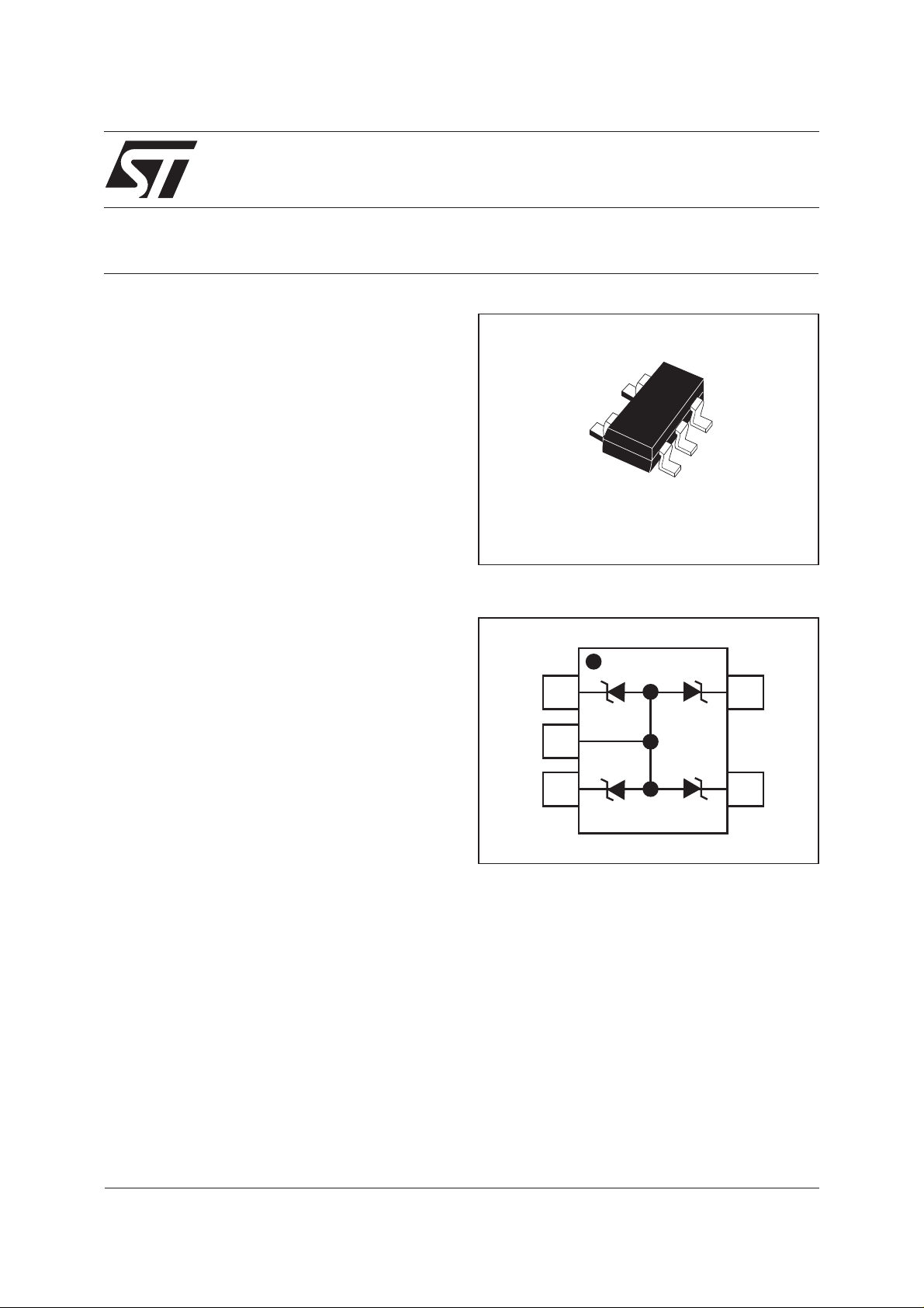
The ESDALC6V1W5 is a 4-bit wide monolithic
suppressor which is designed to protect component
connected to data and transmission lines against
ESD.
It clamps the voltage just above the logic level
supply for positive transients, and to a diode drop
below ground for negative transients.
= 6.1V min
BR
QUAD TRANSIL™ ARRAY
FOR ESD PROTECTION
SOT323-5L
FUNCTIONAL DIAGRAM
I/01
GND
I/02
I/04
I/03
BENEFITS
■
High ESD protection level : up to 25 kV.
■
Capacitance: 12pF @ 0V Typ.
■
High integration.
■
Suitable for high density boards.
COMPLIESWITH THE FOLLOWINGSTANDARDS :
■
IEC61000-4-2 level 4: 15 kV (air discharge)
8kV(contactdischarge)
■
MIL STD 883C-Method 3015-6 : class 3.
(human body model) 25kV (HBM)
June 2002 - Ed: 4A
1/9
ESDALC6V1W5
ABSOLUTE MAXIMUM RATINGS (T
amb
= 25°C)
Symbol Parameter Test conditions Value Unit
V
PP
P
PP
T
j
T
stg
T
op
ELECTRICAL CHARACTERISTICS (T
ESD discharge - MIL STD 883E - Method 3015-7
IEC61000-4-2 air discharge
IEC61000-4-2 contact discharge
Peak pulse power (8/20 µs)
Junction temperature
Storage temperature range
Operating temperature range
= 25°C)
amb
±25
±15
±8
25 W
150 °C
-55to+150 °C
-40to+150 °C
Symbol Parameter
I
V
RM
V
BR
V
CL
Stand-off voltage
Breakdown voltage
Clamping voltage
kV
I
RM
I
PP
C
Rd
Types VBR@I
ESDALC6V1W5
Note 1 : Square pulse Ipp = 15A, tp=2.5µs.
Note 2 : ∆ VBR= αT* (Tamb -25°C) * VBR(25°C)
Leakage current
Peak pulse current
Capacitance per line
Dynamic resistance
min. max. max. typ. max. typ. max.
VVmAµAVm
6.1 7.2 1 1 3 1100 6 7.5 9.5
R
V
V
CL
slope : 1 / R
IRM@V
RM
V
RM
BR
I
RM
I
R
d
Rd αTC C
note 1 note 2 3V bias 3V bias
Ω10
I
PP
-4
/°C pF pF
V
2/9
ESDALC6V1W5
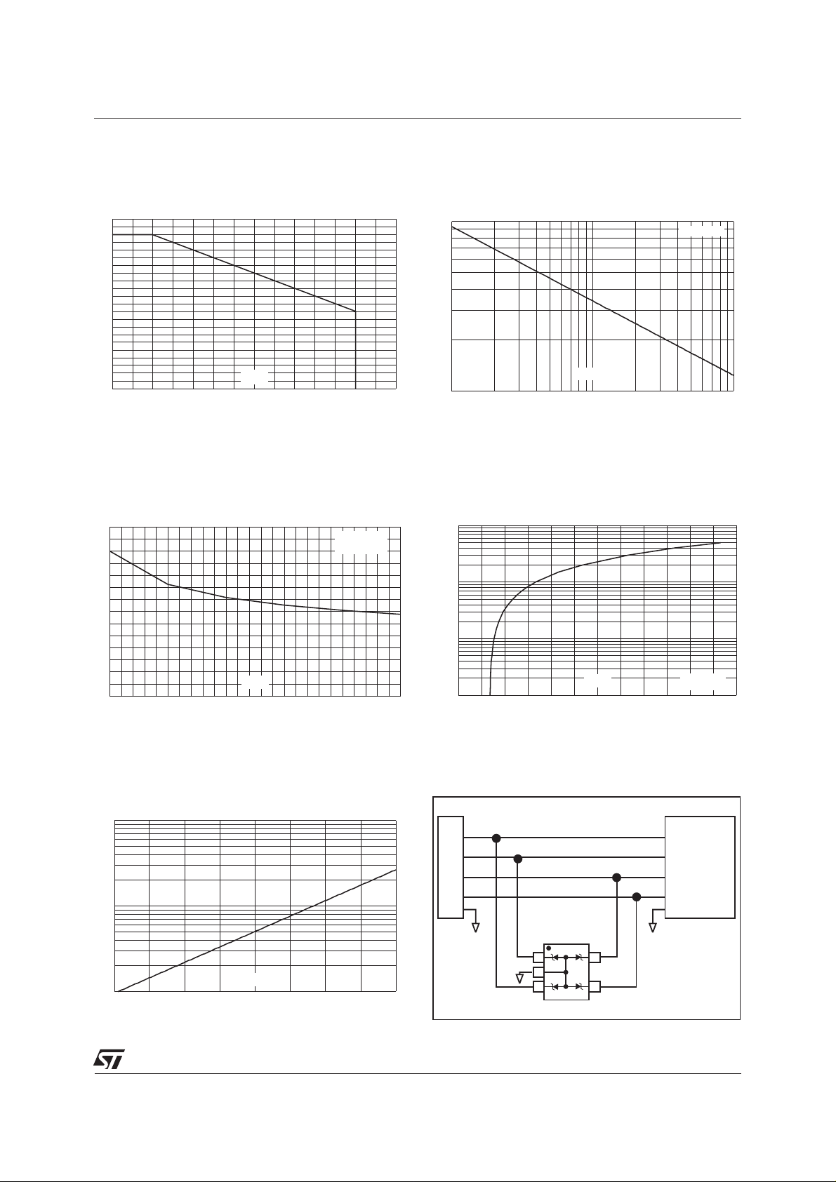
Fig. 1: Relative variation of peak pulse power
versus initial junction temperature.
Ppp[Tj initial] / Ppp [Tj initial = 25°C]
1.1
1.0
0.9
0.8
0.7
0.6
0.5
0.4
0.3
0.2
0.1
0.0
0 25 50 75 100 125 150 175
Tj(°C)
Fig. 3: Junction capacitance versus reverse voltage
applied (typical values).
C(pF)
14
12
F=1MHz
Vosc=30mV
Tj=25°C
RMS
Fig. 2: Peak pulse power versusexponential pulse
duration.
Ppp(W)
100
tp(µs)
10
1 10 100
Tj initial = 25°C
Fig. 4: Clamping voltage versus peak pulse current (maximum values, rectangular waveform).
Ipp(A)
100.0
10
8
6
4
2
0
012345
VR(V)
Fig. 5: Relative variation of leakage current versus
junction temperature (typical values).
IR [Tj] / IR [Tj=25°C]
100
10
1
25 50 75 100 125
Tj(°C)
10.0
1.0
Vcl(V)
0.1
0 102030405060
tp=2.5µs
Tj initial =25°C
Fig. 6: Application example
I/02
I/01
Connector
I/04
I/03
IC
to be
protected
3/9

ESDALC6V1W5
TECHNICAL INFORMATION
1. ESD protection by ESDALC6V1W5
With the focus of lowering the operation levels, the problem of malfunction caused by the environment is
critical. Electrostatic discharge (ESD) is a major cause of failure in electronic systems.
As a transient voltage suppressor, ESDALC6V1W5 is an ideal choice for ESD protection by suppressing
ESDevents. It is capableof clamping theincoming transient toa low enough levelsuch that anydamage is
prevented on the device protected by ESDALC6V1W5.
ESDALC6V1W5 serves as a parallel protection elements, connected between the signal line and ground.
As the transient rises above the operating voltage of the device, the ESDALC6V1W5 becomes a low
impedance path diverting the transient current to ground.
The clamping voltage is given by the following formula:
=VBR+ Rd.I
V
CL
As shown in figure A1, the ESD strikes are clamped by the transient voltage suppressor.
Fig. A1: ESD clamping behavior
G
R
I
PP
PP
Rd
R
V
G
V
BR
V(i/o)
ESD surge ESDALC6V1W5
Tohave a goodapproximation of the remainingvoltages at both Vi/o side, we providethe typical dynamical
resistance value Rd. By taking into account the following hypothesis:
Rg > Rd and Rload > Rd
we have:
Vi o V R
/ =+×
()
The results of the calculation done Vg = 8kV, Rg = 330Ω (IEC61000-4-2 standard), V
Rd = 1.1Ω (typ.) give:
V i o Volts
/,=32 8
()
This confirms the very low remaining voltage across the device to be protected. It is also important to note
that in this approximation the parasitic inductance effect was not taken into account. This could be a few
tenths of volts during a few ns at the Vi/o side.
BR d
V
R
g
g
L OAD
Device
to be
protected
= 6.1V (min) and
BR
4/9

ESDALC6V1W5
Fig. A2: ESD test board
Fig. A3: ESD test configuration
TEST BOARD
V(i/o)
V(i/o)
± 8kV
ESD Contact
discharge
The measurements done here after show very clearly (Fig. A4) the high efficiency of the ESD protection:
the clamping voltage V(i/o) becomes very close to +V
Fig. A4b).
Fig. A4: Remaining voltage during ESD surge
(positive way, Fig. A4a) and -VBR(negative way,
BR
I/O1, I/O2, I/O3 or I/O4
V(i/o)
B2
V(i/o)
a: Response in the positive way b: Response in the negative way
V(i/o)
5/9

ESDALC6V1W5
CROSSTALK BEHAVIOR
Fig. A5: Crosstalk phenomenon
RG1
V
G1
RG2
VG2
Line 1
Line 2
R
L1
R
L2
αβ
αβ
V+ V
1G1 12G2
V+ V
2G2 21G1
DRIVERS RECEIVERS
Thecrosstalk phenomena are dueto the coupling between 2lines. Coupling factors ( β12or β21 ) increase
when the gap across lines decreases, particularly in silicon dice. In the example above, the expected
signal on load R
the V
phenomenon has to be taken into account when the drivers impose fast digital data or high frequency
analog signals. The perturbed line will be more affected if it works with low voltage signal or high load
impedance (few kΩ)
signal represents the effect of the crosstalk phenomenon of the line 1 on the line 2. This
G1
is α2VG2, in fact the real voltage at this point has got an extra value β21VG2. This part of
L2
Fig. A6: Analog crosstalk measurements
RF TEST BOARD
TEST BOARD
To Port1
To Port1To Port1
6/9
I/O4
I/O4
I/O1
I/O1
To Port2
To Port2To Port2

ESDALC6V1W5
Fig. A7: Typical analog crosstalk measurements.
ESDALC6V1W5 :typical analog crosstalk response
0.00
dB
-10.00
-20.00
-30.00
-40.00
-50.00
-60.00
-70.00
-80.00
-90.00
-100.0
1.0M 3.0M 10.0M 30.0M 100.0M 300.0M 1.0G 3.0G
Figure A6gives the measurement circuit for the analog crosstalk application. In figure A7, the curve shows
the effect of the line I/O1 on the line I/O4. In usual frequency range of analog signals (up to 100MHz) the
effect on disturbed line is less than -60dB.
f/Hz
Fig. A8: Digital crosstalk measurements configu-
Fig. A9: Digital crosstalk results.
ration.
0 - 3kV
pulse generator
F= 5MHz
R
t = 3ns
I/O1
V
G1
I/O4
unloaded
GND
β21 G1V
unloaded
VG1
β21 G1V
rise time: t = 3ns
10-90%
crosstalk
Figure A8 shows the measurement circuit used to quantify the crosstalk effect in a classical digital
application.
Figure A9 shows that in such a condition, the impact on the disturbed lineis less than 50mV peak to peak.
No data disturbance was noted on the concerned line. The measurements performed with falling edges
give an impact within the same range.
7/9

ESDALC6V1W5
Fig. A10: Aplac model
I/O1
caphole
Rhole
I/O2
Lbond
Lhole
D6V1
D6V1
D6V1
Lbond
LbondLbond D6V1
I/O4
I/O3
Cz 9.2pF
Rs 100m
Lbond 1.2nH
Lhole 380pH
Caphole 0.2pF
Rhole 450m
Model D6V1
BV = 7
IBV = 1m
CJO = Cz
M = 0.3333
RS = 1
VJ = 0.6
TT = 100n
ORDER CODE
ESDA LC 6V1 W5
ESD ARRAY
LOW CAPACITANCE
V min
BR
Ordering type Marking Package Weight Base qty Delivery mode
ESDALC6V1W5 C61 SOT323-5L 5.4 mg. 3000 Tape & reel
8/9
PACKAGE: SOT323-5L

ESDALC6V1W5
PACKAGE MECHANICAL DATA
SOT323-5L
DIMENSIONS
A1
H
Q1
c
FOOT PRINT (in millimeters)
0.3mm
1mm
1mm
0.35mm
D
ee
b
2.9mm
A2A
REF.
Millimeters Inches
Min. Max. Min. Max.
A 0.8 1.1 0.031 0.043
A1 0 0.1 0 0.004
A2 0.8 1 0.031 0.039
b 0.15 0.3 0.006 0.012
c 0.1 0.18 0.004 0.007
D 1.8 2.2 0.071 0.086
E
E 1.15 1.35 0.045 0.053
e 0.65 Typ. 0.026 Typ.
H 1.8 2.4 0.071 0.094
Q1 0.1 0.4 0.004 0.016
Mechanical specifications
Lead plating Tin-lead
Lead plating thickness 5µm min.
25 µm max.
Lead material Sn / Pb
(70% to 90% Sn)
Lead coplanarity 10µm max.
Body material Moldedepoxy
Epoxy meets UL94,V0
Informationfurnishedis believed to be accurate and reliable. However, STMicroelectronics assumes no responsibility for theconsequencesof
useof such information nor for any infringement of patents orother rights of third parties which may result from itsuse. No license is granted by
implication or otherwise under any patent or patent rights of STMicroelectronics. Specifications mentioned in this publication are subject to
change without notice. This publication supersedes and replaces all information previously supplied.
STMicroelectronics products are not authorized for use as critical components in life support devices or systems without express written approval of STMicroelectronics.
The ST logo is a registered trademark of STMicroelectronics
© 2002 STMicroelectronics - Printed in Italy - All rights reserved.
STMicroelectronics GROUP OF COMPANIES
Australia - Brazil - Canada - China - Finland - France - Germany
Hong Kong - India - Israel - Italy - Japan - Malaysia - Malta - Morocco - Singapore
Spain - Sweden - Switzerland - United Kingdom - United States.
http://www.st.com
9/9
 Loading...