

ESDA6V1S3
ApplicationSpecificDiscretes
A.S.D.
APPLICATIONS
Where transient overvoltage protection in ESD
sensitiveequipment isrequired,suchas :
-COMPUTERS
-PRINTERS
-COMMUNICATIONSYSTEMS
-GSMHANDSETSANDACCESSORIES
-OTHERTELEPHONESETS
FEATURES
18 UNIDIRECTIONALTRANSIL FUNCTIONS
LOWLEAKAGECURRENT: I
200 W PEAKPULSEPOWER(8/20µs)
max.<2 µA
R
ESDA6V2S6
TRANSIL ARRAY
FOR ESD PROTECTION
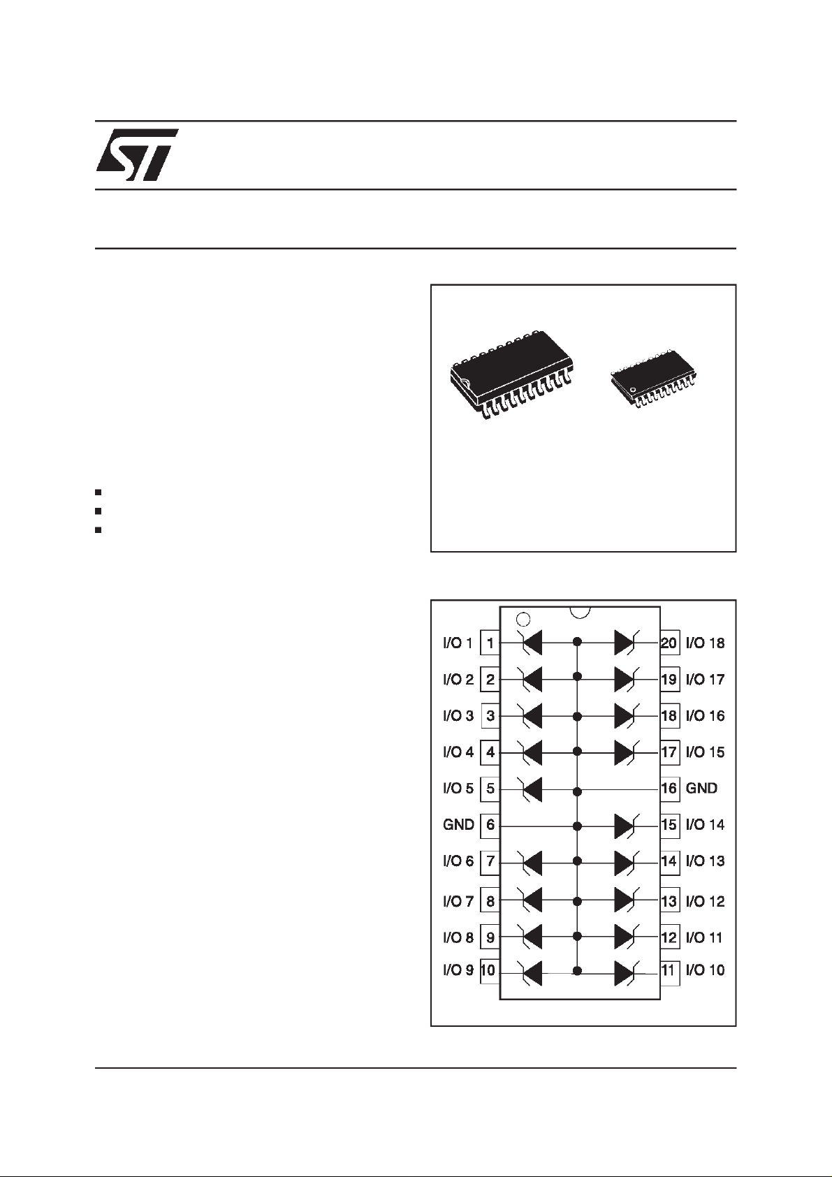
SO20
ESDA6V1S3
SSOP20
ESDA6V2S6
DESCRITION
The ESDA6xxSx is a monolithic voltage
suppressordesignedto protectcomponentswhich
are connected to data and transmission lines
againstESD.
It clamps the voltage just above the logic level
supply for positive transients, and to a diode drop
belowground for negative transients.
BENEFITS
HighESDprotection level: upto 25 kV
Highintegration
Suitablefor highdensityboards
COMPLIESWITH THEFOLLOWING STANDARDS :
IEC1000-4-2: level4
MILSTD883C-Method3015-6: class3
(humanbodymodel)
FUNCTIONALDIAGRAM
October 1998 Ed: 2A
1/7
ESDA6V1S3 / ESDA6V2S6
ABSOLUTEMAXIMUM RATINGS(T
amb
=25°C)
Symbol Parameter Value Unit
V
PP
Electrostaticdischarge
25 kV
MILSTD883C- Method3015-6
P
PP
T
stg
T
j
T
L
ELECTRICALCHARACTERISTICS
Peakpulse power(8/20µs) 200 W
Storagetemperaturerange
Maximumjunction temperature
- 55 to +150
150
Maximumlead temperatureforsolderingduring 10s 260 °C
(T
=25°C)
amb
Symbol Parameter
V
RM
V
BR
V
CL
I
RM
Stand-offvoltage
Breakdownvoltage
Clampingvoltage
Leakagecurrent
°C
°C
I
PP
α
T Voltagetemperaturecoefficient
Peak pulsecurrent
C Capacitance
Rd Dynamicresistance
V
F
Types VBR@I
ESDA6V1S3
ESDA6V2S6
Note 1: Betweenany I/O pin and Ground
Note 2: Square pulse, IPP= 25A forESDA6V1S3and IPP= 15Afor ESDA6V2S6 , tp= 2.5µs
Note 3: ∆VBR= αT*[T
Forwardvoltagedrop
I
R
min. max. max. typ. max. typ. max.
note1 note1 note 2 note 3 0V bias
VVmAµAV
6.1 7.2 1 2 5.25 0.5 6 120 1.25 200
6.2 7.2 1 2 5.25 0.5 6 100 1.25 200
-25] * VBR(25°C)
amb
RM
@V
RM
Rd
Ω10
TC V
α
-4
/°CpF V mA
@I
F
F
2/7
CALCULATION OF THECLAMPING VOLTAGE
USEOFTHEDYNAMICRESISTANCE
TheESDAfamilyhasbeen designed to clamp fast
spikes like ESD. Generally the PCB designers
need to calculate easily the clamping voltageV
CL
This is why we give the dynamic resistance in
addition to the classical parameters. The voltage
across the protection cell can be calculated with
thefollowingformula:
V
CL=VBR
+RdI
PP
WhereIppisthepeakcurrentthroughtheESDAcell.
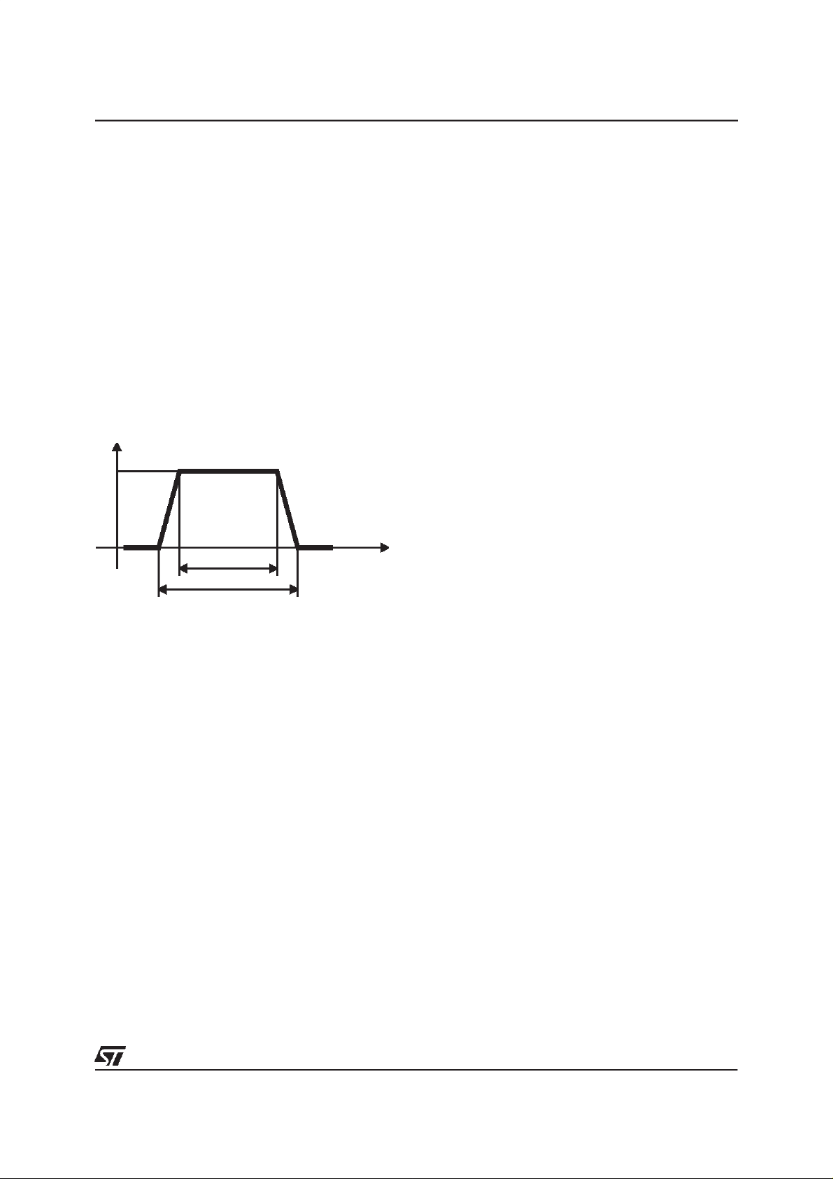
DYNAMICRESISTANCEMEASUREMENT
Theshortdurationof the ESDhasled us toprefer
amoreadaptedtestwave,asbelowdefined,tothe
classical8/20µs and 10/1000µssurges.
I
Ipp
ESDA6V1S3 / ESDA6V2S6
As the value of the dynamic resistance remains
stable for a surge duration lower than 20µs, the
.
2.5µsrectangularsurgeis welladapted.Inaddition
bothrise and fall times are optimized to avoid any
parasiticphenomenonduring the measurementof
Rd.
2µs
tp = 2.5µs
2.5µsdurationmeasurementwave.
t
3/7

ESDA6V1S3 / ESDA6V2S6
Fig. 1
junctiontemperature.
: Peak power dissipation versus initial
Fig. 2 :
Peak pulse power versus exponential
pulseduration(Tj initial = 25 °C).
Ppp[Tj initial]/Pp[Tjinitial=25°C]
1.1
1.0
0.9
0.8
0.7
0.6
0.5
0.4
0.3
0.2
0.1
0.0
0 25 50 75 100 125 150
Tj initial(°C)
Fig. 3 : Clamping voltage versus peak pulse
current(Tj initial =25 °C).
Rectangularwaveformtp= 2.5 µs.
Ipp(A)
50.0
10.0
tp=2.5µs
Ppp(W)
2000
1000
100
10
1 10 100
tp(µs)
Fig. 4 : Capacitance versus reverse applied
voltage(typicalvalues).
C(pF)
100
F=1MHz
Vosc=30mV
50
1.0
V (V)CL
0.1
4 6 8 10 12 14 16 18 20 22 24 26 28 30 32
Fig.5 : Relativevariationof leakagecurrentversus
junctiontemperature(typicalvalues).
RR
I [Tj] / I [Tj=25°C]
200
100
10
Tj(°C)
1
25 50 75 100 125
20
V (V)R
10
12 510
Fig. 6 :
Peak forward voltage drop versus peak
forwardcurrent (typicalvalues).
I (A)
FM
5.00
Tj=25°C
1.00
0.10
V (V)FM
0.01
0.0 0.5 1.0 1.5 2.0 2.5 3.0 3.5
4/7

APPLICATIONEXAMPLE :
1 - Protectionof logic-level signals.
(ex: centronicsjunction)
ESDA6V1S3 / ESDA6V2S6
2 - Protectionof symmetricalsignals.
Note: Capacitancevaluebetween any I/Opinand
Groundis dividedby2.
D1
D2
Dn
0to5V
0to5V
0to5V
A1
A2
A16
+/- 2.5 V
+/- 2. 5 V
+/- 2.5 V
ImplementingitsASD
TM
technology,SGS-Thomson
hasdevelopedamonolithicTRANSILdiodearray,
which is a reliable protection against electrostatic
overloads for computer I/O ports, modems, GSM
handsetsand accessoriesor othersimilar systems
with data outputs. The ESDAxxSx integrates 18
TRANSILdiodesin acompactpackagethat canbe
easily mounted close to the circuitry to be
protected, eliminating the assembly costs
associated with the use of discrete diodes, and
alsoincreasingsystemreliability.
EachTRANSILhas abreakdownvoltage between
6.2V (minimum) and 7.2V (maximum). When the
inputvoltageis lower than the breakdown voltage,
the diodes present a high impedance to ground.
For short overvoltage pulses, the fast-acting
diodesprovide analmostinstantaneousresponse,
clampingthe voltageto a safe level.
5/7

ESDA6V1S3 / ESDA6V2S6
ORDER CODE
ESD ARRAY
ESDA 6V1 S 3 RL
min
V
BR
PACKAGING:
RL =Tape andreel
= Tube
PACKAGE :
3 : SO20
6 : SSOP20
MARKING :
Logo,date code
TYPE MARKING
ESDA6V1S3 E6V1S3
ESDA6V2S6 ESDA6V2S6
Packaging :
Preferredpackagingis tapeand reel.
PACKAGEMECHANICAL DATA
SO20 (Plastic)
D
A
K
e
A1B
DIMENSIONS
REF.
Millimeters Inches
Min. Typ. Max. Min. Typ. Max.
hx45°
A 2.35 2.65 0.092 0.104
A1 0.10 0.20 0.004 0.008
L
C
B 0.33 0.51 0.013 0.020
C 0.23 0.32 0.009 0.013
D 12.6 13.0 0.484 0.512
Weight:
6/7
0.55g.
EH
E 7.40 7.60 0.291 0.299
e 1.27 0.050
H 10.0 10.65 0.394 0.419
h 0.25 0.75 0.010 0.029
L 0.50 1.27 0.020 0.050
K8°(max)

PACKAGEMECHANICAL DATA
SSOP20 (Plastic)
L
2
A
A
b
D
20
e
11
101
k
E1
E
A1 c
ESDA6V1S3 / ESDA6V2S6
DIMENSIONS
REF.
A 2.00 0.079
A1 0.25 0.010
A2 1.51 2.00 0.059 0.079
b 0.25 0.30 0.35 0.010 0.012 0.014
c 0.10 0.35 0.004 0.014
D 7.05 8.05 0.278 0.317
E 7.60 8.70 0.299 0.343
E1 5.02 6.10 6.22 0.198 0.240 0.245
e 0.65 0.026
k0° 10° 0° 10°
L 0.25 0.50 0.80 0.010 0.020 0.031
Millimeters Inches
Min. Typ. Max. Min. Typ. Max.
Weight:
Informationfurnished is believedto beaccurate andreliable. However, STMicroelectronics assumesno responsibilityfor the consequences of
use ofsuch informationnor forany infringementof patentsor otherrights ofthirdparties which mayresult fromits use. No license isgranted by
implication or otherwise under any patent or patent rights of STMicroelectronics. Specifications mentioned in this publication are subject to
change withoutnotice. This publicationsupersedes and replaces all informationpreviouslysupplied.
STMicroelectronics products are not authorized for use as critical components in lifesupport devices or systems without express written approval of STMicroelectronics.
0.18g.
The ST logo is a registered trademarkof STMicroelectronics
1998STMicroelectronics - Printed in Italy - Allrightsreserved.
STMicroelectronics GROUP OF COMPANIES
Australia - Brazil - Canada - China - France - Germany- Italy - Japan - Korea - Malaysia - Malta - Mexico - Morocco -
The Netherlands -Singapore -Spain - Sweden - Switzerland - Taiwan - Thailand - UnitedKingdom - U.S.A.
http://www.st.com
7/7
 Loading...