

®
ESDA6V1W5
Application Specific Discretes
A.S.D.
MAIN APPLICATIONS
Where transient overvoltage protection in ESD
sensitive equipment is required, such as :
Computers
Printers
Communication systems
GSM handsets and ac cessories
Other telephone sets
Set top boxes
FEATURES
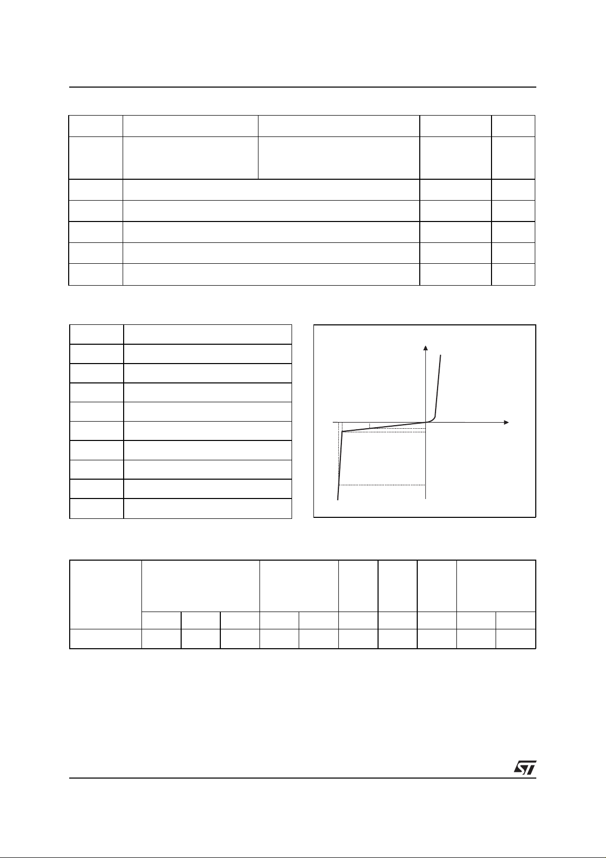
4 unidirectional TRANSIL functions.
Breakdown voltage : VBR = 6.1 V min.
Low leakage current : < 1µA.
Very low PC B spac e consuming : 4.2 mm2 typically.
DESCRIPTION
The ESDA6V1W5 is a 4-bit wide monolithic
suppressor which is designed to protect component
connected to data and transmission lines against
ESD.
It clamps the voltage just above the logic level
supply for positive transients, and to a diode drop
below ground for negative transients.
QUAL TRANSIL ARRAY
FOR ESD PROTECTION
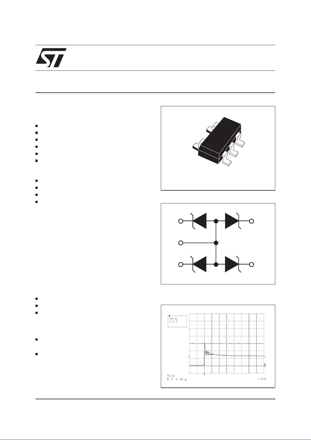
SOT323-5L
FUNCTIONAL DIAGRAM
1
2
3
5
4
BENEFITS
High ESD protection level : up to 25 kV.
High integration.
Suitable for high density boards.
COMPLIES WITH THE FOLLOWING STANDARDS :
IEC 1000-4-2 level 4
MIL STD 883C-Method 3015-6 : class 3.
(human body model)
September 1999 - Ed: 1A
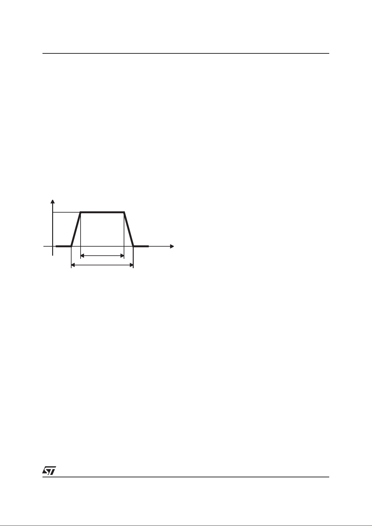
ESD RESPONSE TO IEC1000-4-2
(air discharge 16 kV , p ositive surge)
1/7
ESDA6V1W5
ABSOLUTE MAXIMUM RATINGS
(T
amb
= 25° C)
Symbol Parameter Test conditions Value Unit
V
PP
P
PP
T
op
T
j
T
stg
T
L
ELECTRICAL CHARACTERISTICS
ESD discharge MIL STD 883C - Method 3015-6
IEC1000-4-2, air discharge
IEC1000-4-2, contact discharge
25
16
9
Peak pulse power (8/20 µs) 150 W
Operating temperature range - 40 to + 85 °C
Junction temperature 150 °C
Storage temperature range - 55 to + 150 °C
Lead solder temperature (10 secondes duration) 260 °C
(T
= 25°C)
amb
Symbol Parameter
V
RM
V
BR
V
CL
Stand-off voltage
Breakdown voltage
Clamping voltage
I
kV
I
RM
I
PP
α
T Voltage temperature coefficient
Leakage current
Peak pulse current
C Capacitance per line
Rd Dynamic resistance
V
F
Types VBR @ I
ESDA6V1W5
note 1
: Square pulse Ipp = 15A, tp=2.5µs.
note 2
: ∆ VBR = αT* (Tamb -25°C) * VBR (25°C)
Forward voltage drop
min. max. max. typ. max. typ. max.
VVmA
6.1 7.2 1 1 3 350 6 90 1.25 200
R
V
V
CL
I
@ V
RM
AVm
µ
RM
V
BR
slope : 1 / R
Rd
note 1 note 2 0V bias
Ω
RM
I
RM
I
R
d
TC V
α
10-4/°CpF V mA
I
PP
@ I
F
V
F
2/7
CALCULATION OF THE CLAMPING VOLTAGE
USE OF THE DY NAM IC RE SIS TANCE
The ESDA family has been des igned t o c lamp fast
spikes like ESD. Generally the PCB designers
need to calculate easily the clamping voltage V
CL
This is why we give the dynamic resistance in
addition to the classical parameters. The voltage
across the protection cell can be calculated with
the following formula:
= VBR + Rd I
V
CL
PP
Where Ipp is the peak current through the ESDA cell.
DYNAMIC RESISTANCE MEAS UREMENT
The short duration of the ESD has led us to prefer
a more adapted test wave, as below defined, to the
classical 8/20µs and 10/1000µs surges.
I
Ipp
ESDA6V1W5
.
2µs
tp = 2.5µs
2.5µs duration measurement wave.
As the value of the dynamic resistance remains
stable for a surge duration lower than 20µs, the
2.5µs rectangular surge is well adapted. In addition
both rise and fall times are optimized to avoid any
parasitic phenomenon during the measurement of
Rd.
t
3/7

ESDA6V1W5
Fig. 1 :
Peak power dissipation versus initial
junction temperature
Ppp[Tj initial]/Pp p [T j in itia l= 2 5 °C]
1.1
1.0
0.9
0.8
0.7
0.6
0.5
0.4
0.3
0.2
0.1
0.0
0 25 50 75 100 125 150 175
Fig. 3 :
Clamping voltage versus peak pulse
Tj initial(°C)
current (Tj initial = 25 °C).
Rectangular waveform tp = 2.5 µs.
Ipp(A)
50.0
tp=2.5µs
10.0
1.0
0.1
0 5 10 15 20 25 30
Vcl(V)
Fig. 2 :
Peak pulse power versus exponential
pulse duration (Tj initial = 25 °C)
Ppp(W)
1000
100
10
1 10 100
Fig. 4 :
Capacitance versus reverse applied
tp(µs)
voltage (typical values).
C(pF)
90
80
70
60
50
40
30
20
10
1.0 1.5 2.0 2.5 3.0 3.5 4.0 4.5 5.0
VR(V)
F=1MHz
Vosc=30mV
Fig. 5
: Relative variation of leak age c urrent
versus junction temperature (typical values).
IR[Tj] / IR[Tj=25°C ]
5
4
3
2
1
25 50 75 100 125 150
4/7
Tj(°C)
Fig. 6 :
Peak forward voltage drop versus peak
forward current (typical values).
IFM(A)
1E+0
Tj=25°C
1E-1
1E-2
1E-3
0.6 0.7 0.8 0.9 1.0 1.1 1.2 1.3 1.4
VFM(V)

ESDA6V1W5
1. ESD protection by the ESDA6V1W5
With the focus of lowering the operation levels, the problem of m alfunction caus ed by the environment is
critical. Electrostatic discharge (ESD) is a major cause of failure in electronic system.
Transient Voltage Suppressors are an ideal choice for ESD protection and have proven capable in
suppressing ESD events. They are capable of clamping the incoming transient to a low enough level such
that damage to the protected semiconductor is prevented.
Surface mount TVS arrays offer the best choice for minimal lead inductance.
They serve as parallel protection elements, connected between the signal line to ground. As the transient
rises above the operating voltage of the device, the TVS array becomes a low impedance path diverting the
transient current to ground.
A
Keyboard
terminal
printer
etc
I / O
B
FUNCTIONAL
DECODER
C
D
The ESDA6V1W5 array is the ideal product for use as board level protection of ESD sensitive
semiconductor components.
The tiny SOT323-5L package makes the ESDA6V1W5 device some of the smallest ESD protection
devices available. It also allows design flexibility in the design of "crowded" boards where the space saving
is at a premium. This enables to shorten the routing and can contribute to improved ESD performance.
2. Circuit Board L ayou t
Circuit board layout is a critical design step in the suppression of ESD induced transients. The following
guidelines are recommended :
The ESDA6V1W5 should be placed as near as possible to the input terminals or connectors.
Minimise the path length between the ESD suppressor and the protected device
Minimise all conductive loops, including power and ground loops
The ESD transient return path to ground should be kept as short as possible.
Use ground planes whenever possible.
5/7

ESDA6V1W5
ORDER CODE
ESDA 6V1 W5
ESD ARRAY
PACKAGE : SOT323-5L
VBR min
Ordering type Marking Package Weight Base qty Delivery mode
ESDA6V1W5 E61 SOT323-5L 5.4 mg. 3000 Tape & reel
PACKAGE ME CHANICAL D AT A
SOT323-5L
DIMENSIONS
A1
REF.
A2A
A 0.8 1.1 0.031 0.043
Millimeters Inches
Min. Max. Min. Max.
A1 0 0.1 0 0.004
A2 0.8 1 0.031 0.039
D
ee
b 0.15 0.3 0.006 0.012
c 0.1 0.18 0.004 0.007
Q1
FOOT PRINT
6/7
H
c
(in millimeters)
0.3mm
1mm
1mm
0.35mm
b
29mm
D 1.8 2.2 0.071 0.086
E 1.15 1.35 0.045 0.053
E
e 0.65 Ty p. 0.026 Typ.
H 1.8 2.4 0.071 0.094
Q1 0.1 0.4 0.004 0.016
Mechanical specifications
Lead plating Tin-lead
Lead plating thickness 5µm min.
25 µm max.
Lead material Sn / Pb
(70% to 90% Sn)
Lead coplanarity 10µm max.
Body material M olded epoxy
Epoxy meets UL94,V0

ESDA6V1W5
Information furnished is believed to be accurate and reliable. However, STMicroelectronics assumes no responsibility for the consequences of
use of such information nor for any infringement of patents or other rights of third parties which may result from its use. No license is granted by
implication or otherwi se un der any pat ent or patent rights of STMic roelec tronics. S pecifications ment ioned in t his publ ication are subject to
change without notice. This publication supersedes and replaces all information previously supplied.
STMicroelectronics products are not authorized for use as critical components in li fe s upport devices or systems without express written approval of STMicroelectronics.
The ST logo is a registered trademark of STMicroe lectronics
© 1999 STMicroelectronics - Printed in Italy - All rights reser ved.
STMicroelectronics GROUP OF COMPANIES
Australia - Brazil - China - Finland - France - Germany - Hong Kong - India - Italy - Japan - Malaysia
Malta - Morocco - Singapore - Spain - Sweden - Switzerland - United Kingdom - U.S.A.
http://www.st.com
7/7
 Loading...