

SGS Thomson Microelectronics ESDA6V1SC6, ESDA6V1SC5, ESDA25SC6, ESDA5V3SC6, ESDA5V3SC5 Datasheet
...
ESDAxxSC5
®
ESDAxxSC6
Application Specific Discretes
A.S.D.
APPLICATIONS
Where transient overvoltage protection in ESD
sensitive equipment is required, such as :
-COMPUTERS
- PRINTERS
- COMMUNICATION SYSTEMS
- GSM HANDSETS AND ACCESSORIES
- OTHER TELEPHONE SET
FEATURES
4 UNIDIRECTIONAL TRANSIL FUNCTIONS
n
LOW LEAKAGE CURRENT: IRmax. < 20 µAat
n
V
BR
n
500 W PEAK PULSE POWER (8/20 µs)
DESCRIPTION
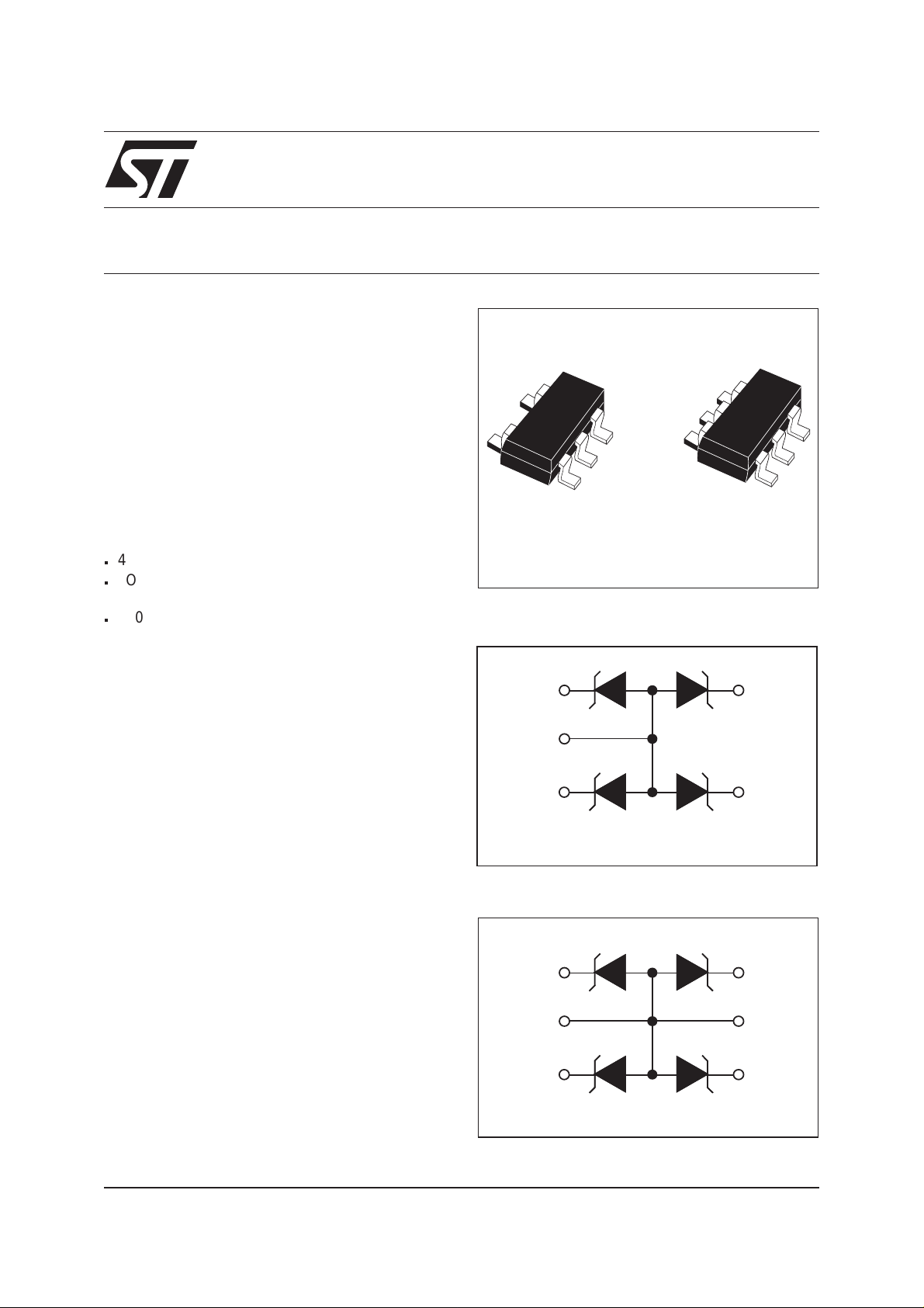
QUAD TRANSIL ARRAY
FOR ESD PROTECTION
SOT23-5L (SC-59)
ESDAxxSC5
FUNCTIONAL DIAGRAM
SOT23-5L
SOT23-6L (SC-59)
ESDAxxSC6
The ESDAxxSC5 and ESDAxxSC6 are monolithic
voltage suppressors designed to protect
components which are connected to data and
transmission lines against ESD.
They clamp the voltage just above the logic level
supply for positive transients, and to a diode drop
below ground for negative transient.
BENEFITS
High ESD protection level : up to 25 kV
High integration
Suitable for high density boards
COMPLIES WITH THE FOLLOWING STANDARDS:
IEC61000-4-2 : level 4
MIL STD 883C-Method 3015-6 : class3
(human body model)
1
2
3
SOT23-6L
1
2
3
5
4
6
5
4
March 2000 Ed: 5D
1/7
ESDAxxSC5 / ESDAxxSC6
ABSOLUTE MAXIMUM RATINGS (T
amb
= 25°C)
Symbol Test conditions Value Unit
V
PP
P
PP
T
j
T
stg
T
L
T
op
note 1: 300 W for ESDA14V2SC5 AND ESDA14V2SC6
note 2: Evolution of functional parameters is given by curves.
ELECTRICAL CHARACTERISTICS (T
Symbol Parameter
V
RM
V
BR
V
CL
I
RM
I
PP
αT
C
Rd
V
F
ESD discharge - MIL STD 883C - Method 3015-6
IEC61000-4-2 air discharge
IEC61000-4-2 contact discharge
Peak pulse power (8/20µs) note1
Junction temperature
Storage temperature range
Lead solder temperature (10 second duration)
Operating temperature range
= 25°C)
amb
Stand-off voltage
Breakdown voltage
V
Clamping voltage
BR
Leakage current
Peak pulse current
Voltage temperature coefficient
Capacitance
Dynamic resistance
Slope:
Forward voltage drop
25
16
9
500 W
150 °C
-55 to +150 °C
260 °C
-40 to +125 °C
I
I
F
I
I
RM
PP
V
F
V
RM
1
Rd
kV
V
@IRIRM@V
V
BR
min. max. max. typ. max. typ. max.
Types
VVmAµAVmΩ10
ESDA5V3SC5
5.3 5.9 1 2 3 230 5 280 1.25 200
ESDA5V3SC6
ESDA6V1SC5
6.1 7.2 1 20 5.25 350 6 190 1.25 200
ESDA6V1SC6
ESDA14V2SC5
14.2 15.8 1 5 12 650 10 100 1.25 200
ESDA14V2SC6
ESDA25SC6
note 1 : Square pulse, Ipp = 15A, tp=2.5µs.
note 2 : ∆ VBR= αT* (Tamb -25°C) * VBR(25°C)
2/7
25 30 1 1 24 1000 10 60 1.2 10
Rd αTCV
RM
note 1 note 2 0V bias
-4
/°C pF V mA
@I
F
F

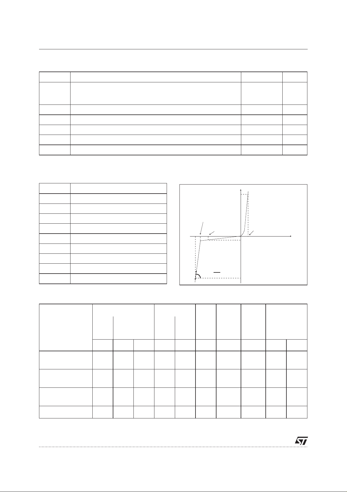
CALCULATION OF THE CLAMPING VOLTAGE
USE OF THE DYNAMIC RESISTANCE
The ESDA familyhasbeendesigned to clamp fast
spikes like ESD. Generally the PCB designers
need to calculate easily the clamping voltage V
CL
This is why we give the dynamic resistance in
addition to the classical parameters. The voltage
across the protection cell can be calculated with
the following formula:
VCL=VBR+RdI
PP
WhereIppisthepeak currentthrough theESDA cell.
DYNAMIC RESISTANCE MEASUREMENT
The short duration of the ESDhasledusto prefer
amoreadapted testwave, as belowdefined, tothe
classical 8/20µs and 10/1000µs surges.
I
Ipp
ESDAxxSC5 / ESDAxxSC6
As the value of the dynamic resistance remains
stable for a surge duration lower than 20µs, the
.
2.5µs rectangular surge is well adapted. In
addition both rise and fall times are optimized to
avoid any parasitic phenomenon during the
measurement of Rd.
2µs
tp = 2.5µs
2.5µs duration measurement wave.
t
3/7
 Loading...