ESDA6V1S3
ApplicationSpecificDiscretes
A.S.D.
APPLICATIONS
Where transient overvoltage protection in ESD
sensitiveequipment isrequired,suchas :
-COMPUTERS
-PRINTERS
-COMMUNICATIONSYSTEMS
-GSMHANDSETSANDACCESSORIES
-OTHERTELEPHONESETS
FEATURES
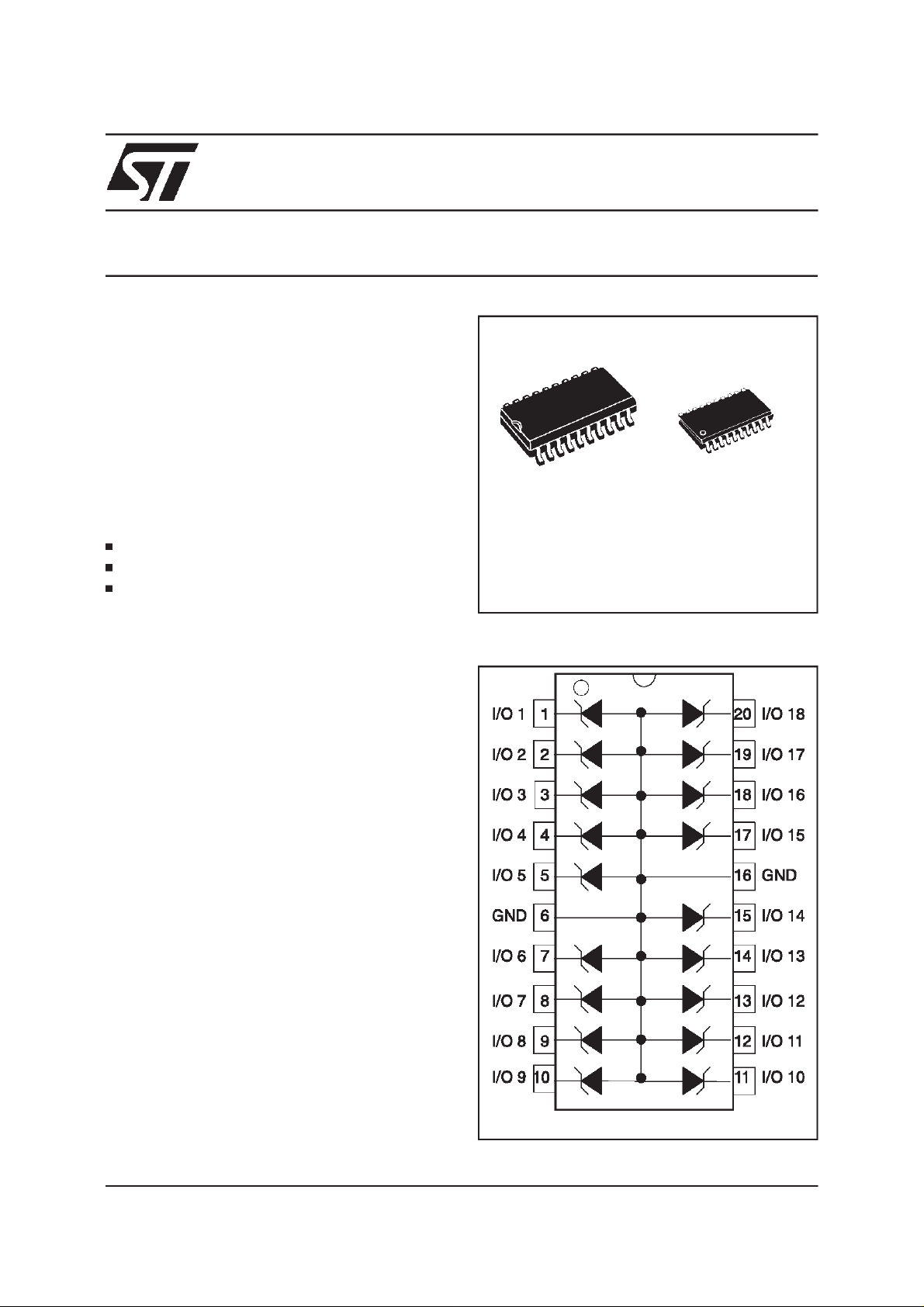
18 UNIDIRECTIONALTRANSIL FUNCTIONS
LOWLEAKAGECURRENT: I
200 W PEAKPULSEPOWER(8/20µs)
max.<2 µA
R
ESDA6V2S6
TRANSIL ARRAY
FOR ESD PROTECTION
SO20
ESDA6V1S3
SSOP20
ESDA6V2S6
DESCRITION
The ESDA6xxSx is a monolithic voltage
suppressordesignedto protectcomponentswhich
are connected to data and transmission lines
againstESD.
It clamps the voltage just above the logic level
supply for positive transients, and to a diode drop
belowground for negative transients.
BENEFITS
HighESDprotection level: upto 25 kV
Highintegration
Suitablefor highdensityboards
COMPLIESWITH THEFOLLOWING STANDARDS :
IEC1000-4-2: level4
MILSTD883C-Method3015-6: class3
(humanbodymodel)
FUNCTIONALDIAGRAM
October 1998 Ed: 2A
1/7

ESDA6V1S3 / ESDA6V2S6
ABSOLUTEMAXIMUM RATINGS(T
amb
=25°C)
Symbol Parameter Value Unit
V
PP
Electrostaticdischarge
25 kV
MILSTD883C- Method3015-6
P
PP
T
stg
T
j
T
L
ELECTRICALCHARACTERISTICS
Peakpulse power(8/20µs) 200 W
Storagetemperaturerange
Maximumjunction temperature
- 55 to +150
150
Maximumlead temperatureforsolderingduring 10s 260 °C
(T
=25°C)
amb
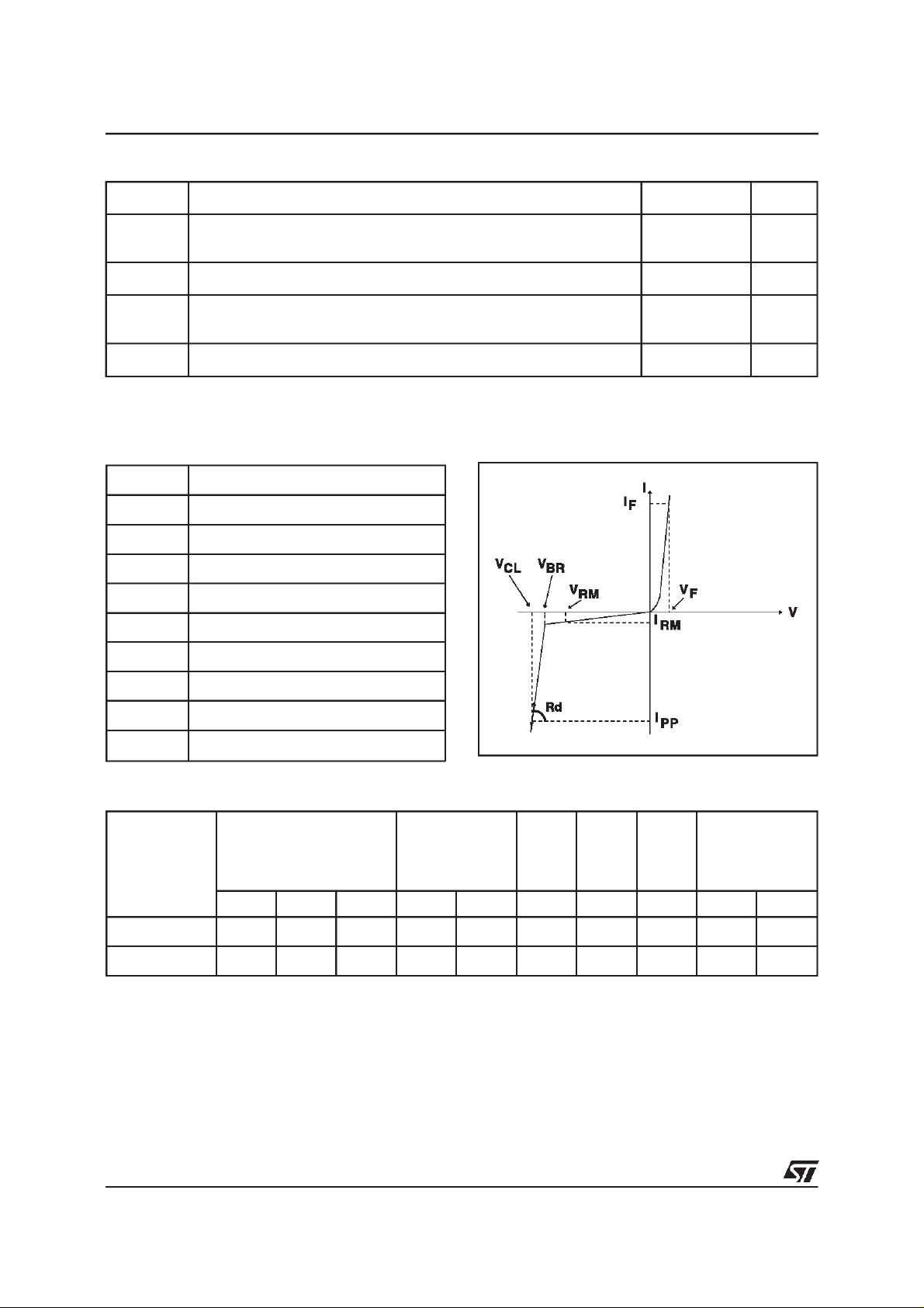
Symbol Parameter
V
RM
V
BR
V
CL
I
RM
Stand-offvoltage
Breakdownvoltage
Clampingvoltage
Leakagecurrent
°C
°C
I
PP
α
T Voltagetemperaturecoefficient
Peak pulsecurrent
C Capacitance
Rd Dynamicresistance
V
F
Types VBR@I
ESDA6V1S3
ESDA6V2S6
Note 1: Betweenany I/O pin and Ground
Note 2: Square pulse, IPP= 25A forESDA6V1S3and IPP= 15Afor ESDA6V2S6 , tp= 2.5µs
Note 3: ∆VBR= αT*[T
Forwardvoltagedrop
I
R
min. max. max. typ. max. typ. max.
note1 note1 note 2 note 3 0V bias
VVmAµAV
6.1 7.2 1 2 5.25 0.5 6 120 1.25 200
6.2 7.2 1 2 5.25 0.5 6 100 1.25 200
-25] * VBR(25°C)
amb
RM
@V
RM
Rd
Ω10
TC V
α
-4
/°CpF V mA
@I
F
F
2/7

CALCULATION OF THECLAMPING VOLTAGE
USEOFTHEDYNAMICRESISTANCE
TheESDAfamilyhasbeen designed to clamp fast
spikes like ESD. Generally the PCB designers
need to calculate easily the clamping voltageV
CL
This is why we give the dynamic resistance in
addition to the classical parameters. The voltage
across the protection cell can be calculated with
thefollowingformula:
V
CL=VBR
+RdI
PP
WhereIppisthepeakcurrentthroughtheESDAcell.
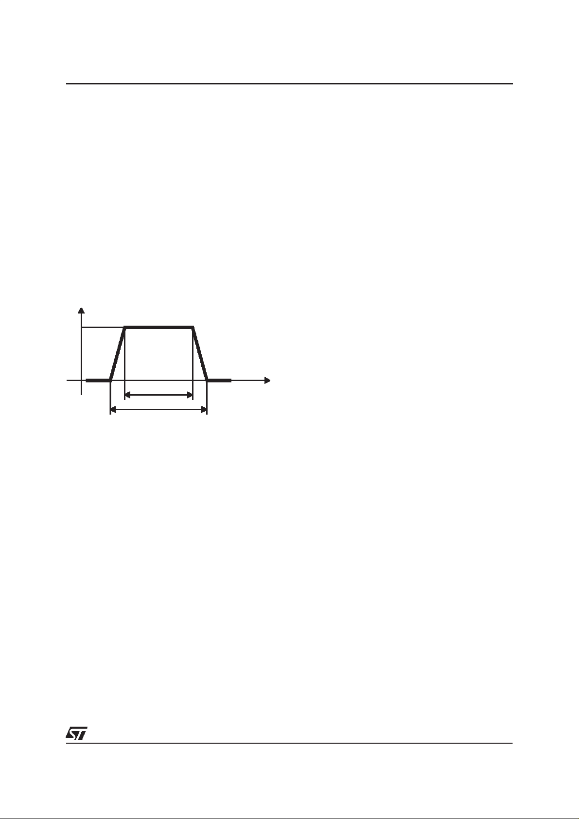
DYNAMICRESISTANCEMEASUREMENT
Theshortdurationof the ESDhasled us toprefer
amoreadaptedtestwave,asbelowdefined,tothe
classical8/20µs and 10/1000µssurges.
I
Ipp
ESDA6V1S3 / ESDA6V2S6
As the value of the dynamic resistance remains
stable for a surge duration lower than 20µs, the
.
2.5µsrectangularsurgeis welladapted.Inaddition
bothrise and fall times are optimized to avoid any
parasiticphenomenonduring the measurementof
Rd.
2µs
tp = 2.5µs
2.5µsdurationmeasurementwave.
t
3/7
 Loading...