®
ESDA6V1P6
Application Specific Discretes
A.S.D.
MAIN APPLICATIONS
Where transient overvoltage protection in ESD
sensitive equipment is required, such as :
Computers
■
Printers
■
Communication systems and cellular phones
■
Video equipment
■
Thisdeviceisparticularlyadpatedto the protection
of symmetrical signals.
FEATURES
4UNIDIRECTIONAL TRANSIL™ FUNCTIONS.
■
■ BREAKDOWN VOLTAGE V
■ LOW LEAKAGE CURRENT < 500 nA
VERY SMALL PCB AREA < 2.6 mm
■
DESCRIPTION
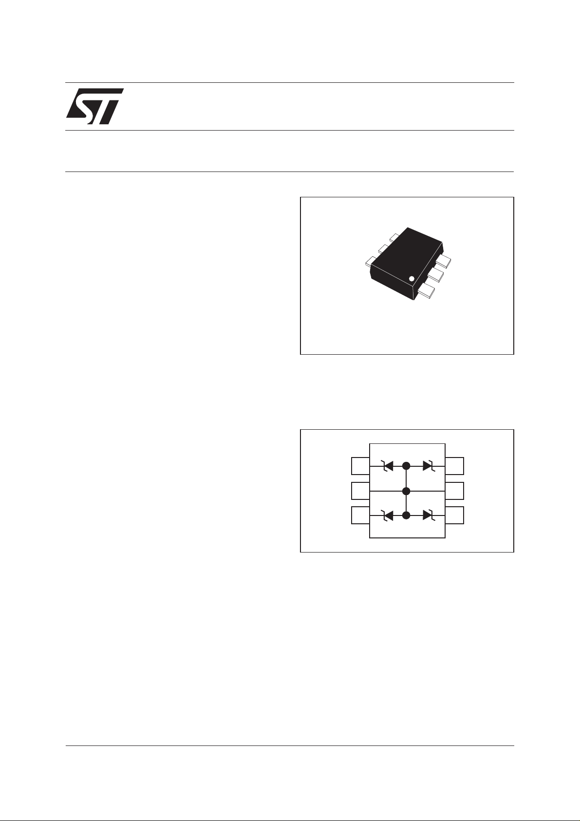
The ESDA6V1P6 is a monolithic array designed to
protect up to 4 lines against ESD transients.
This device is ideal for applications where board
space saving is required.
= 6.1V MIN
BR
2
QUAD TRANSIL™ ARRAY
FOR ESD PROTECTION
SOT-666
FUNCTIONAL DIAGRAM
1
6
BENEFITS
■
High ESD protection level.
■
High integration.
■
Suitable for high density boards.
COMPLIESWITH THE FOLLOWING STANDARDS:
■
IEC61000-4-2 level 4: 15 kV (air discharge)
8kV (contact discharge)
■
MIL STD 883E-Method 3015-7: class 3
25kV HBM (Human Body Model)
January 2003 - Ed: 2
2
3
5
4
1/8

ESDA6V1P6
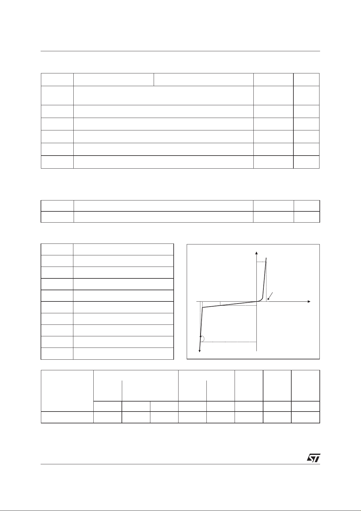
ABSOLUTE RATINGS (T
amb
= 25°C)
Symbol Parameter Test conditions Value Unit
V
PP
P
PP
T
j
T
stg
T
L
T
op
Note 1: for a surge greater than the maximum values, the diode will fail in short-circuit.
ESD discharge - IEC61000-4-2 air discharge
IEC61000-4-2 contact discharge
Peak pulse power (8/20 µs) (see note 1) Tjinitial = Tamb
Junction temperature
Storage temperature range
Maximum lead temperature for soldering during 10s at 5mm for case
Operating temperature range
±15
±8
150 W
125 °C
-55to+150 °C
260 °C
-40to+150 °C
THERMAL RESISTANCES
Symbol Parameter Value Unit
R
th(j-a)
ELECTRICAL CHARACTERISTICS (T
Junction to ambient on printed circuit on recommended pad layout
= 25°C)
amb
220 °C/W
kV
Symbol Parameter
V
RM
V
BR
V
CL
I
RM
I
PP
αT
V
F
C
R
d
Types V
ESDA6V1P6
Stand-off voltage
Breakdown voltage
Clamping voltage
Leakage current
Peak pulse current
Voltage tempature coefficient
Forward voltage drop
Capacitance per line
Dynamic resistance
BR
min. max. max. typ. max. typ.
VVmAµAV
6.1 7.2 1 0.5 3 1.5 4.5 70
@I
R
V
CLVBRVRM
Slope: 1/R
IRM@V
RM
I
I
F
V
F
I
RM
d
I
PP
Rd αTC
@0V
Ω10
-4
/°C pF
V
2/8

ESDA6V1P6
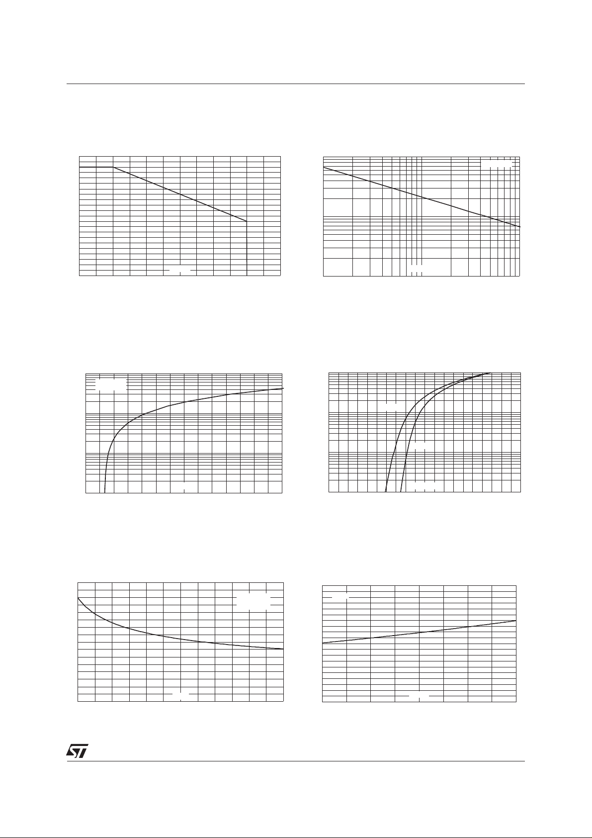
Fig. 1: Relative variation of peak pulse power
versus initial junction temperature.
P [T initial] / P [T initial=25°C)
PP j PP j
1.1
1.0
0.9
0.8
0.7
0.6
0.5
0.4
0.3
0.2
0.1
0.0
0 25 50 75 100 125 150
T (°C)
j
Fig. 3: Clamping voltage versus peak pulse
current (typical values, rectangular waveform).
I (A)
PP
100.0
t =2.5µs
p
T initial=25°C
j
Fig. 2:Peak pulse power versusexponentialpulse
duration.
P (W)
PP
1000
100
T (µs)
10
1 10 100
p
T initial=25°C
j
Fig. 4: Forward voltage drop versus peak forward
current (typical values).
I (A)
FM
1.E+00
10.0
1.0
V (V)
0.1
0 10203040506070
CL
Fig. 5: Junction capacitance versus reverse
voltage applied (typical values).
C(pF)
80
70
60
50
40
30
20
10
0
0123456
V (V)
R
F=1MHz
V =30mV
OSC RMS
T=25°C
j
T=125°C
1.E-01
1.E-02
1.E-03
0.0 0.2 0.4 0.6 0.8 1.0 1.2 1.4 1.6 1.8 2.0
j
T=25°C
j
V (V)
FM
Fig. 6: Relative variation of leakage current versus
junction temperature (typical values).
I [T ] / I [T =25°C]
Rj Rj
2.0
V =3V
R
1.8
1.6
1.4
1.2
1.0
0.8
0.6
0.4
0.2
0.0
25 50 75 100 125
T (°C)
j
3/8
 Loading...