


®
ESDAxxL
Application Specific Discretes
A.S.D.
APPLICATIONS
Where transient overvoltage protection in ESD
sensitive equipment is required, such as :
- COMPUTERS
- PRINTERS
- COMMUNICATION SYSTEMS
It is particulary recommended for the RS232 I/O
port protection where the line interface withstands
only with 2kV ESD surges.
FEATURES
2 UNIDIRECTIONAL TRANSIL FUNCTIONS.
n
LOW LEAKAGE CURRENT : IRmax. < 20µAat
n
.
V
BR
300 W PEAK PULSE POWER (8/20µs)
n
DESCRIPTION
The ESDAxxL is a dual monolithic voltage
suppressordesignedtoprotectcomponentswhich
are connected to data and transmission lines
against ESD.
It clamps the voltage just above the logic level
supply for positive transients, and to a diode drop
below ground for negative transients.
It can also work as bidirectionnal suppressor by
connecting only pin1 and 2.
DUAL TRANSIL ARRAY
FOR ESD PROTECTION
SOT23
FUNCTIONAL DIAGRAM
BENEFITS
High ESD protection level : up to 25 kV.
High integration.
Suitable for high density boards.
COMPLIESWITHTHEFOLLOWINGSTANDARDS :
IEC61000-4-2 level 4
MIL STD 883C-Method 3015-6 : class 3.
(human body model)
Marchr 2000 - Ed: 4A
1/6
ESDAxxL
ABSOLUTE MAXIMUM RATINGS (T
amb
= 25°C)
Symbol Parameter Value Unit
V
PP
P
PP
T
stg
T
j
T
L
T
op
note 1: Evolution of functional parameters is given by curves.
ELECTRICAL CHARACTERISTICS (T
Symbol Parameter
V
RM
V
BR
V
CL
I
RM
I
PP
Electrostatic discharge
MIL STD 883C - Method 3015-6
IEC61000-4-2 air discharge
IEC61000-4-2 contact discharge
Peak pulse power (8/20 µs)
Storage temperature range
Maximum junction temperature
Maximum lead temperature for soldering during 10s
Operating temperature range
= 25°C)
amb
Stand-off voltage
Breakdown voltage
Clamping voltage
Leakage current
V
BR
V
Peak pulse current
RM
25
16
9
300 W
-55to+150
150
260 °C
-40to+125 °C
I
I
F
V
F
I
RM
kV
°C
°C
V
αT
C
Rd
V
F
Types VBR@
ESDA5V3L
ESDA6V1L
ESDA14V2L
ESDA25L
note 1 : Square pulse Ipp = 15A, tp=2.5µs.
note 2 : ∆ VBR= αT* (Tamb -25°C) * VBR(25°C)
Voltage temperature coefficient
Capacitance
Dynamic resistance
Forward voltage drop
min. max. max. typ. max. typ. max.
VVmAµAV
5.3 5.9 1 2 3 280 5 220 1.25 200
6.1 7.2 1 20 5.25 350 6 140 1.25 200
14.2 15.8 1 5 12 650 10 90 1.25 200
25 30 1 1 24 1000 10 50 1.2 10
1
Slope:
Rd
I
R
IRM@V
RM
Rd αTC V
note 1 note 2 0V bias
10-4/⊃CpF V mA
Ω
m
I
PP
@I
F
F
2/6

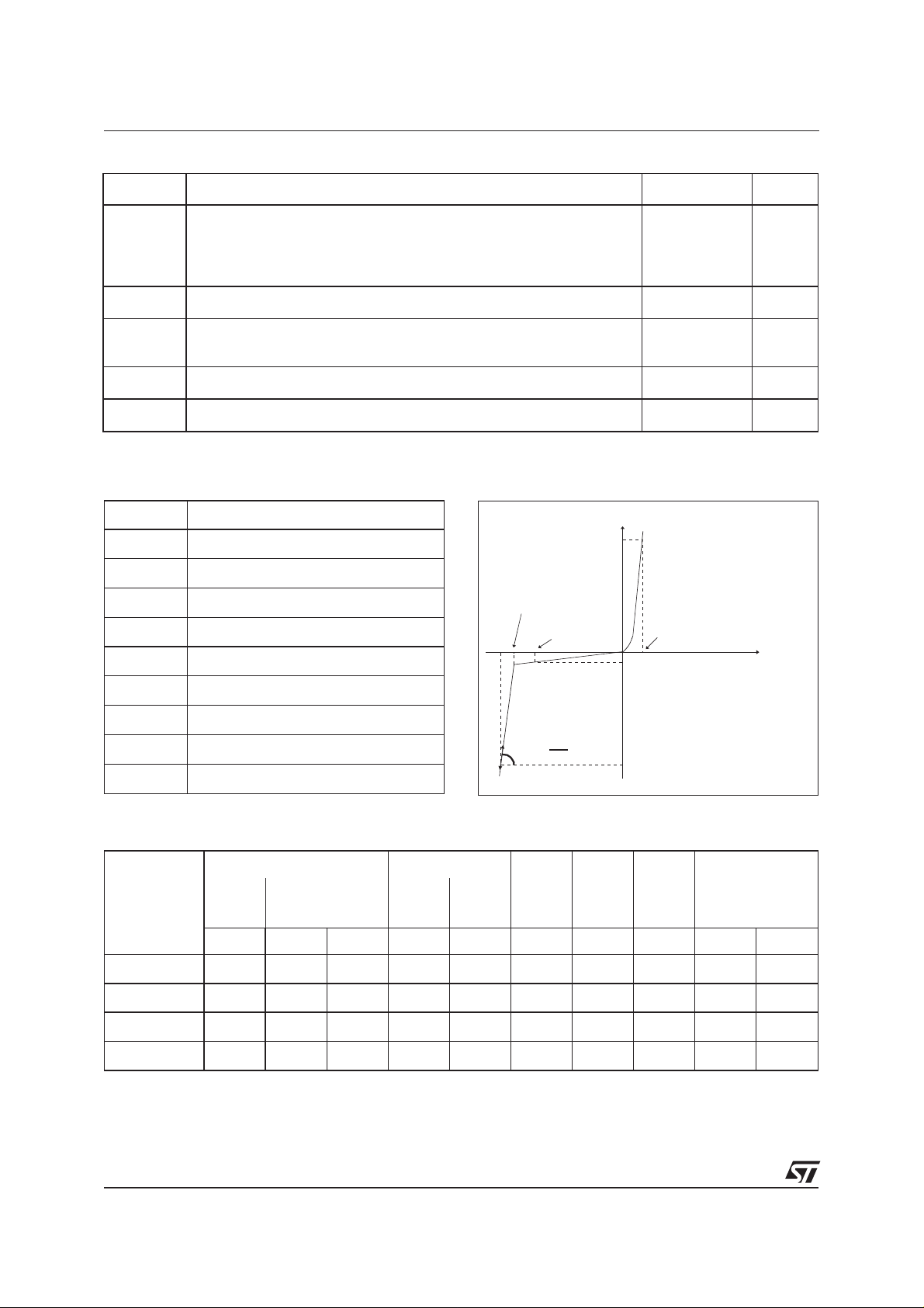
CALCULATION OF THE CLAMPING VOLTAGE
USE OF THE DYNAMIC RESISTANCE
The ESDA family has been designed to clamp fast
spikes like ESD. Generally the PCB designers
need to calculate easily the clamping voltage V
CL
This is why we give the dynamic resistance in
addition to the classical parameters. The voltage
across the protection cell can be calculated with
the following formula:
=VBR+RdI
V
CL
PP
WhereIpp is thepeak current throughthe ESDA cell.
DYNAMIC RESISTANCE MEASUREMENT
The short duration of the ESD has led us to prefer
amore adapted test wave, as below defined, to the
classical 8/20µs and 10/1000µs surges.
I
Ipp
As the value of the dynamic resistance remains
stable for a surge duration lower than 20µs, the
.
2.5µs rectangular surge is well adapted. In
addition both rise and fall times are optimized to
avoid any parasitic phenomenon during the
measurement of Rd.
ESDAxxL
2µs
tp = 2.5µs
2.5µs duration measurement wave.
t
3/6

ESDAxxL
Fig. 1: Peak power dissipation versus initial junc-
tion temperature.
Ppp[Tj initial]/Pp p [T j in itia l= 2 5 °C]
1.1
1.0
0.9
0.8
0.7
0.6
0.5
0.4
0.3
0.2
0.1
0.0
0 25 50 75 100 125 150
Tj initial(°C)
Fig. 3: Clamping voltage versus peak pulse cur-
rent (Tj initial = 25 °C).
Rectangular waveform tp = 2.5 µs.
Ipp(A)
50.0
ESDA5V3L
10.0
1.0
0.1
0 5 10 15 20 25 30 35 40 45 50 55 60 65 70 75 80
ESDA6V1L
ESDA14V2L
Vcl(V)
ESDA25L
tp=2.5µs
Fig. 2: Peak pulse power versus exponential
pulse duration (Tj initial = 25 °C).
Ppp(W)
3000
1000
100
tp(µs)
10
1 10 100
Fig. 4: Capacitance versus reverse applied voltage (typical values).
C(pF)
200
ESDA5V3L
100
ESDA6V1L
50
ESDA14V2L
20
VR(V)
10
12 51020 50
F=1MHz
Vosc=30mV
ESDA25L
Fig. 5: Relative variation of leakage current versus
junction temperature (typical values).
IR[Tj] / IR[Tj=25°C ]
200
100
10
Tj(°C)
1
25 50 75 100 125
4/6
ESDA6V1L
&
ESDA14V2L
ESDA25L
ESDA5V3L
Fig. 6: Peak forward voltage drop versuspeak forward current (typical values).
IFM(A)
5.00
Tj=25°C
1.00
0.10
0.01
0.0 0.5 1.0 1.5 2.0 2.5 3.0 3.5 4.0
ESDA5V3L
ESDA6V1L
VFM(V)
ESDA14V2L
ESDA25L

ESDAxxL
1. ESD protection by the ESDAxxL
Electrostatic discharge (ESD) is a major cause of
failure in electronic systems.
Transient Voltage Suppressors (TVS) are an ideal
choice for ESD protection. They are capable of
clamping the incoming transient to a low enough
level such that damage to the protected
semiconductor is prevented.
Surfacemount TVS arrays offer the best choice for
minimal lead inductance.
They serve as parallel protection elements,
connected between the signal line to ground. As
I/O
I/O
I/O
the transient rises above the operating voltage of
the device, the TVS array becomes a low
impedance path diverting the transient current to
ground.
The ESDAxxL array is the ideal board level
protection of ESD sensitive semiconductor
components.
Thetiny SOT23 package allows design flexibility in
the design of high density boards where the space
savingis at a premium. Thisenables to shorten the
routing and contributes to hardening againt ESD.
I/O
2 * ESDAXXL
2. Circuit Board Layout
Circuit board layout is a critical design step in the
suppression of ESD induced transients. The
following guidelines are recommended :
n
TheESDAxxL should be placed as close as possible to the input terminals or connectors.
n
The path length between the ESD suppressor
and the protected line should be minimized
ESD
sensitive
device
GND
n
All conductive loops, including power and
ground loops should be minimized
n
The ESD transient return path to ground should
be kept as short as possible.
n
Ground planes should be used whenever possible.
5/6

ESDAxxL
ORDER CODE
ESDA 6V1 L
ESD ARRAY
PACKAGE MECHANICAL DATA
SOT23 (Plastic)
E
e
B
e1
S
L
H
PACKAGE : SOT23 PLASTIC
VBRmin
A
REF.
Millimeters Inches
DIMENSIONS
Min. Max. Min. Max.
D
A 0.89 1.4 0.035 0.055
A1 0 0.1 0 0.004
B 0.3 0.51 0.012 0.02
A1
c 0.085 0.18 0.003 0.007
D 2.75 3.04 0.108 0.12
e 0.85 1.05 0.033 0.041
e1 1.7 2.1 0.067 0.083
E 1.2 1.6 0.047 0.063
H 2.1 2.75 0.083 0.108
c
L 0.6 typ. 0.024 typ.
S 0.35 0.65 0.014 0.026
FOOT PRINT (in millimeters)
0.9
0.035
2.35
0.92
Informationfurnishedisbelieved to be accurate and reliable. However, STMicroelectronics assumes no responsibility for the consequences of
useof such information nor for any infringement of patents or otherrightsof third parties which may result from its use. No licenseis granted by
implication or otherwise under any patent or patent rights of STMicroelectronics. Specifications mentioned in this publication are subject to
change without notice. This publication supersedes and replaces all information previously supplied.
STMicroelectronics products are not authorized for use as critical components in life support devices or systems without express written approval of STMicroelectronics.
0.037
1.45
0.075
0.035
0.9
0.035
1.1
0.043
1.9
mm
inch
1.1
0.043
0.9
MARKING
TYPE MARKING
ESDA5V3L EL53
ESDA6V1L EL61
ESDA14V2L EL15
ESDA25L EL25
Packaging: Standard packaging is tape and reel.
The ST logo is a registered trademark of STMicroelectronics
© 2000 STMicroelectronics - Printed in Italy - All rights reserved.
STMicroelectronics GROUP OF COMPANIES
Australia - Brazil - China - Finland - France - Germany - Hong Kong - India - Italy - Japan - Malaysia
Malta - Morocco - Singapore - Spain - Sweden - Switzerland - United Kingdom - U.S.A.
http://www.st.com
6/6
 Loading...