®
ESDA6V1-5W6
Application Specific Discretes
A.S.D.
APPLICATIONS
Where transient overvoltage protection in ESD
sensitive equipment is required, such as :
Computers
n
Printers
n
Communication systems
n
Cellular phone handsets and accessories
n
Other telephone sets
n
Set top boxes
n
DESCRIPTION
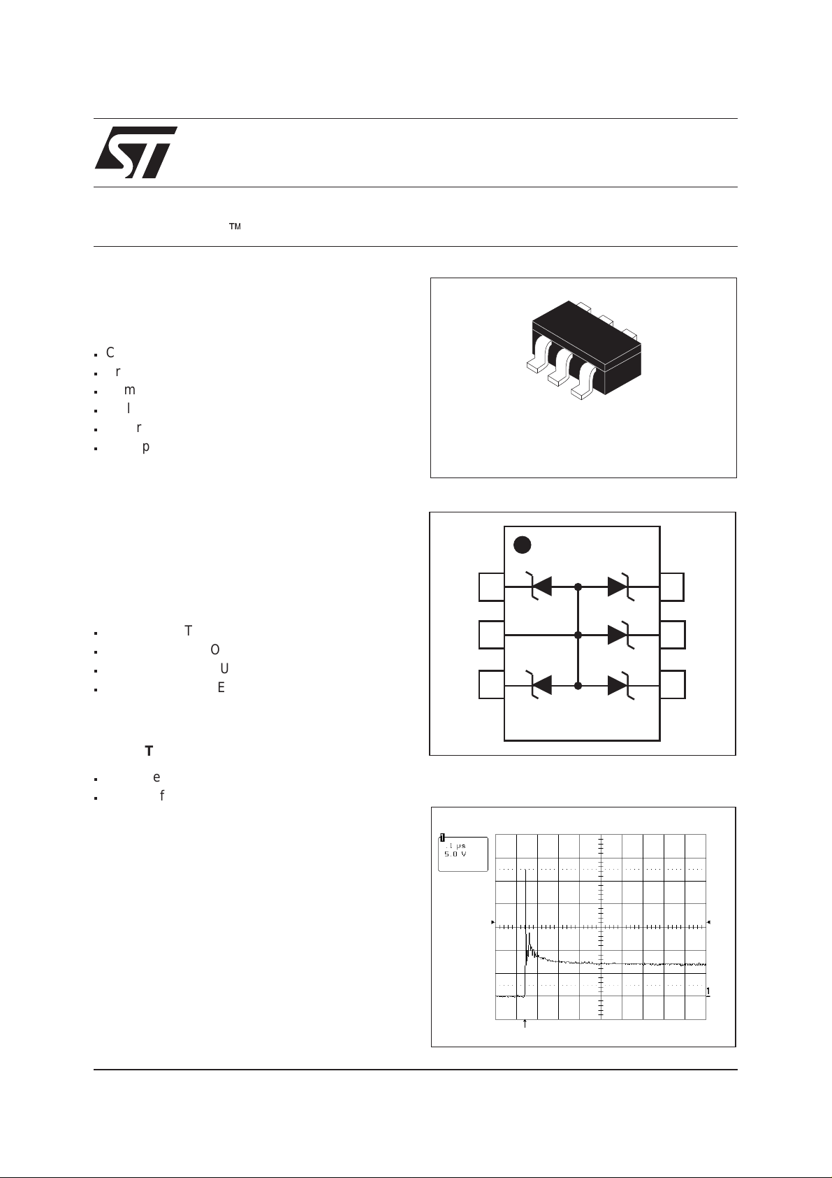
The ESDA6V1-5W6 is a 5-bit wide monolithic
suppressor which is designed to protect
components connected to data and transmission
lines against ESD.
FEATURES
n
5 UNIDIRECTIONAL TRANSIL FUNCTIONS
n
BREAKDOWN VOLTAGE: VBR = 6.1V min
n
LOW LEAKAGE CURRENT: IRmax<1µA
n
VERYSMALL SIZEFOR PCBSPACE SAVING:
4.2mm
2
TYPICALLY
ä
TRANSIL ARRAY
FOR ESD PROTECTION
SOT323-6L
FUNCTIONAL DIAGRAM
I/O1
Gnd
I/O2
I/O5
I/O4
I/O3
BENEFITS
n
High integration
n
Suitable for high density boards
COMPLIES WITH THE FOLLOWING STANDARDS:
- IEC 61000-4-2: level 4
15 kV (air discharge)
8 kV (contact discharge)
- MIL STD 883C-Method 3015-6: class3
(human body model)
March 2000 -Ed: 1A
ESD response to IEC61000-4-2
(air discharge 16kV, positive surge)
1/9

ESDA6V1-5W6
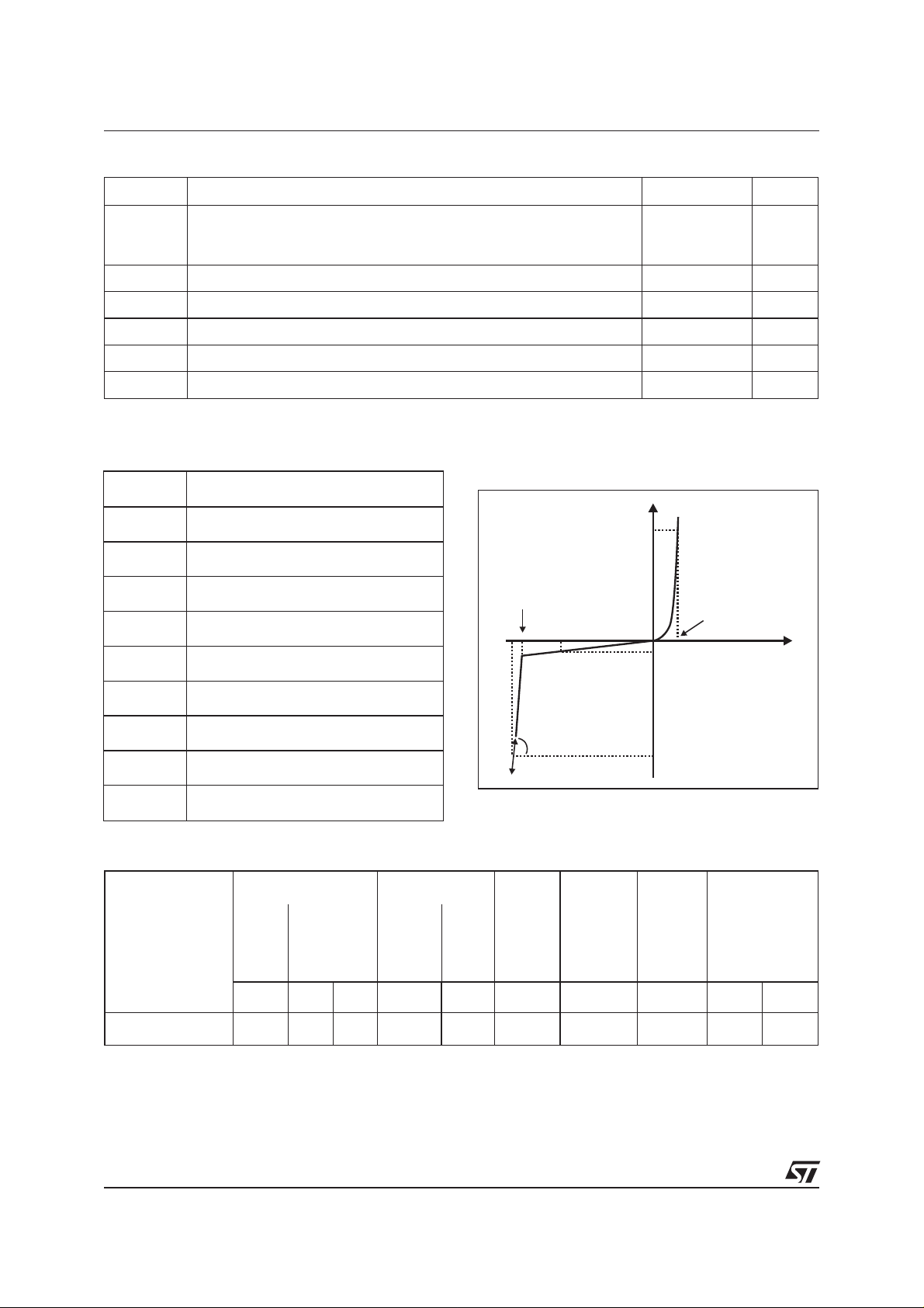
ABSOLUTE MAXIMUM RATINGS (T
amb
= 25°C)
Symbol Test conditions Value Unit
V
PP
P
PP
T
j
T
stg
T
L
T
op
Note 1: The evolution of the operating parameters versus temperature is given by curves and αT parameter.
ELECTRICAL CHARACTERISTICS (T
ESD discharge - MIL STD 883C - Method 3015-6
IEC 61000-4-2 air discharge
IEC 61000-4-2 contact discharge
Peak pulse power (8/20µs)
Junction temperature
Storage temperature range
Lead solder temperature (10 seconds duration)
Operating temperature range (note 1)
= 25°C)
amb
25
20
15
100 W
150 °C
-55 to +150 °C
260 °C
-40 to +125 °C
Symbol Parameter
I
V
RM
V
BR
V
CL
I
RM
I
PP
Stand-off voltage
Breakdown voltage
Clamping voltage
Leakage current
Peak pulse current
Vcl
VBR
IF
VF
VRM
IRM
kV
V
αT
C
Rd
V
F
Voltage temperature coefficient
Capacitance
Dynamic impedance
Forward voltage drop
V
BR@IR
min. max
Type
.
VVmAµAVmΩ10
ESDA6V1-5W6
Note 2 : Square pulse, Ipp = 15A, tp=2.5µs.
Note 3: ∆VBR= αT*(T
6.1 7.2 1 1 3 610 6 50 1.25 200
- 25°C) * VBR(25°C)
amb
Slope = 1/Rd
IPP
IRM@V
RM
Rd αTCV
max. typ. max. typ. max
note 2 note 3 0V bias
-4
/°C pF V mA
F@IF
2/9

ESDA6V1-5W6
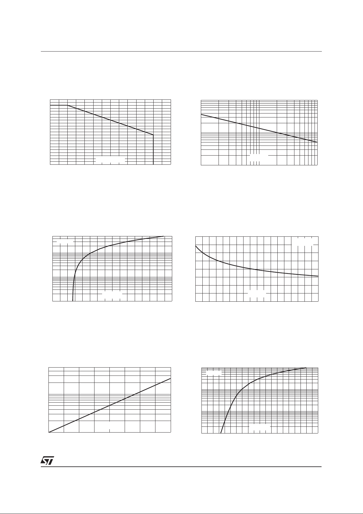
Fig. 1: Peak power dissipation versus initial
junction temperature.
Ppp[Tj initial]/Pp p [T j in itia l= 2 5 °C]
1.1
1.0
0.9
0.8
0.7
0.6
0.5
0.4
0.3
0.2
0.1
0.0
0 25 50 75 100 125 150 175
Tj initial(°C)
Fig. 3: Clamping voltage versus peak pulse current
(Tj initial = 25°C) Rectangular waveform tp = 2.5µs.
Ipp(A)
50.0
tp=2.5µs
10.0
Fig. 2: Peak pulse power versus exponential
pulse duration (Tj initial = 25°C).
Ppp(W)
1000
100
tp(µs)
10
1 10 100
Fig. 4: Capacitance versus reverse applied voltage
(typical values).
C(pF)
50
40
F=1MHz
Vosc=30mV
1.0
Vcl(V)
0.1
0 5 10 15 20 25 30 35 40
Fig. 5: Relative variation of leakage current versus junction temperature (typical values).
IR[Tj] / IR[Tj=25°C]
50
10
Tj(°C)
1
25 50 75 100 125
30
20
VR(V)
10
0.5 1.0 1.5 2.0 2.5 3.0 3.5 4.0 4.5 5.0
Fig. 6: Peak forward voltage drop versus peak
forward current (typical values).
IFM(A)
1E+0
1E-1
1E-2
1E-3
Tj=25°C
VFM(V)
0.6 0.7 0.8 0.9 1.0 1.1 1.2 1.3 1.4 1.5 1.6
3/9
 Loading...