

®
ESDA6V1-4F1
QUAD TRANSIL™ ARRAY
A.S.D.™
APPLICATIONS
Where transient overvoltage protection in ESD
sensitive equipment is required, such as :
Computers
■
Printers
■
Communication systems
■
GSM handsets and accessories
■
Other telephone sets
■
Set top boxes
■
DESCRIPTION
The ESDA6V1-4F1 is a 4-bit wide monolithic
suppressor designed to protect against ESD
components which are connected to data and
transmission lines.
It clamps the voltage just above the logic level
supply for positive transients, and to a diode
forward voltage drop below ground for negative
transients.
FEATURES
■
4 Unirectional transil functions
■
Breakdown voltage: VBR= 6.1Vmin
■
Low leakage current < 10 µA
■
Very low PCB space consuming
FOR ESD PROTECTION
3
A
B
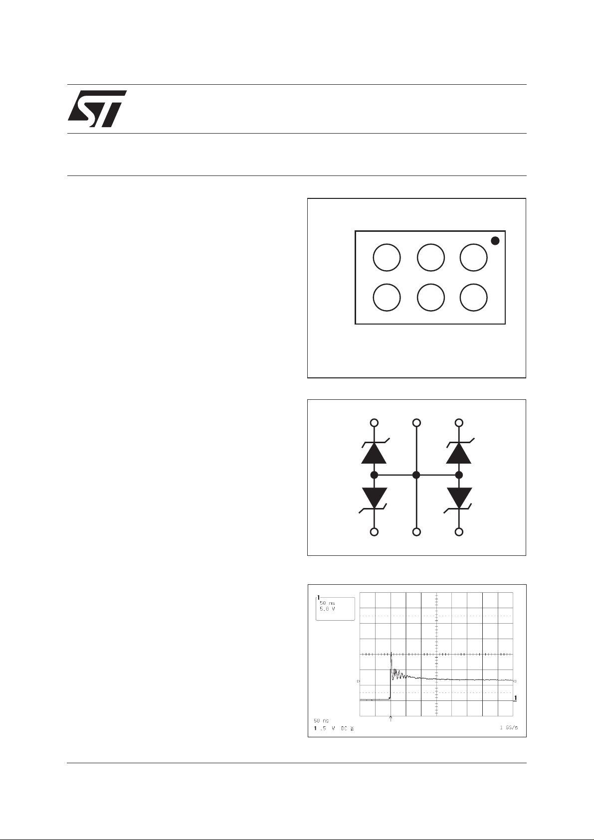
FUNCTIONAL DIAGRAM
Z1
Z2
Flip Chip
(Bump side)
A3
21
GND
GND
Z3
Z4
A1A2
BENEFITS
■
> ± 15kV ESD Protection
■
High integration
■
Suitable for high density boards
COMPLIES WITH THE FOLLOWING STANDARDS:
- IEC61000-4-2: Level 4
15 kV (air discharge)
8 kV (contact discharge)
- MIL STD 883E-Method 3015-6: class3
(Human body model)
July 2002- Ed: 2A
B3
B2 B1
ESD RESPONSE TO IEC61000-4-2
(air discharge 16kV, positive surge)
1/6
ESDA6V1-4F1
ABSOLUTE MAXIMUM RATINGS (T
amb
= 25°C)
Symbol Test conditions Value Unit
V
PP
P
PP
T
j
T
stg
T
L
T
op
ELECTRICAL CHARACTERISTICS (T
ESD discharge - MIL STD 883E - Method 3015-6
IEC61000-4-2 air discharge
IEC61000-4-2 contact discharge
Peak pulse power (8/20µs)
Junction temperature
Storage temperature range
Lead solder temperature (10 seconds duration)
Operating temperature range
= 25°C)
amb
±25
±15
±8
150 W
150 °C
-55 to +150 °C
260 °C
-40 to +85 °C
Symbol Parameter
I
V
RM
V
BR
V
CL
I
RM
I
PP
Stand-off voltage
Breakdown voltage
Clamping voltage
Leakage current
Peak pulse current
VCLVBR VRM
IRM
IR
kV
V
αT Voltage temperature coefficient
C Capacitance per line
Rd Dynamic impedance
V
F
Forward voltage drop
min. max. max. typ. max max
Type
ESDA6V1- 4F1
Note 1: Square pulse IPP= 15A, tp = 2.5µs
Note 2: ∆VBR= αT*(T
-25)*VBR(25°C)
amb
6.1 7.2 1 10 5 350 6 250
Slope = 1/Rd
IPP
V
@I
BR
VVmAµAVmΩ10
R
IRM@V
RM
Rd TC
note 1 note 2 0V bias
-4
/°C pF
2/6

ESDA6V1-4F1
Fig. 1: Peak power dissipation versus initial junc-
tion temperature
Ppp[Tj initial]/Ppp[Tj initial=25°C]
1.1
1.0
0.9
0.8
0.7
0.6
0.5
0.4
0.3
0.2
0.1
0.0
0 25 50 75 100 125 150 175
Tj initial(°C)
Fig. 3: Clamping voltage versus peak pulse current
(Tj initial = 25°C). Rectangular waveform t
Ipp(A)
50.0
tp = 2.5µs
10.0
1.0
Vcl(V)
0.1
0 5 10 15 20 25 30
= 2.5µs.
P
Fig. 2: Peakpulse power versus exponential pulse
duration (Tj initial = 25°C)
Ppp(W)
1000
100
tp(µs)
10
1 10 100
Fig. 4: Capacitance versus reverse applied voltage
(typical values).
C(pF)
250
225
200
175
150
125
100
75
0.0 0.5 1.0 1.5 2.0 2.5 3.0 3.5 4.0 4.5 5.0
VR(V)
F=1MHz
Vosc=30mV
Fig. 5: Relative variation of leakage current versus
junction temperature (typical values).
IR[Tj] / IR[Tj=25°C]
1.8
1.6
1.4
1.2
Tj(°C)
1.0
25 50 75 100 125 150
3/6

ESDA6V1-4F1
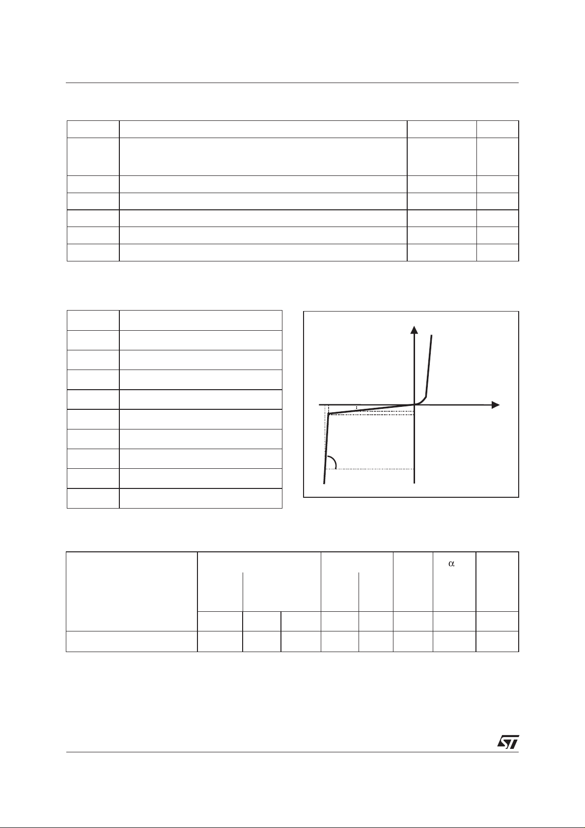
CALCULATION OF THE CLAMPING VOLTAGE
USE OF THE DYNAMIC RESISTANCE
The ESDA6V1-4F1 has been designed to clamp fast spikes like ESD. Generally thePCB designers need
to calculate easily the clamping voltage VCL. This is why we give the dynamic resistance in addition to the
classical parameters.
The voltage across the protection cell can be calculated with the following formula:
VVRI
=+⋅
CL BR d PP
Where IPPis the peak current through the ESDA cell.
DYNAMIC RESISTANCE MEASUREMENT
The short duration of the ESD has led us to prefer a more adapted test wave, as below defined, to the
classical 8/20 µs and 10/1000 µs surges
I
IPP
2µs
2.5 µs
2.5 µs duration measurement wave
tt
As the value of the dynamic resistance remains stable for a surge duration lower than 20µs, the 2.5µs
rectangular surge is well adapted. In addition both rise and fall times are optimised to avoid any parasitic
phenomenon during the measurement of Rd.
ESD PROTECTION WITH ESDA6V1-4F1
With the focus of lowering the operation levels, the problem of malfunction caused by the environment is
critical. Electrostatic discharge (ESD) is a major cause of failure in electronic system.
Transient Voltage Suppressors are an ideal choice for ESD protection and have proven capable in
suppressing ESD events. They are capable of clamping the incoming transient to a low enough level such
that damage to the protected semiconductor is prevented. Surface mount TVS arrays offerthe best choice
forminimal lead inductance. They serveas parallel protection elements, connectedbetween the signal line
to ground. As the transient rises above the operating voltage of the device,the TVS arraybecomes a low
impedance path diverting the transient current to ground.
4/6

ESDA6V1-4F1
Connector
IC to be protected
ESDA6V1-4F1
The ESDA6V1-4F1 array is the ideal product for use as board level protection of ESD sensitive
semiconductor components.
The Flip Chip package makes the ESDA6V1-4F1 device some of the smallest ESD protection devices
available. It also allows design flexibility in the design of “crowded” boards where the space saving is at a
premium. This enables to shorten the routing and can contribute to improved ESD performance.
LAYOUT RECOMMENDATIONS
Copper Pad
Cu - Ni (2-6µm) - Au (0.2µm max)
= 250µm (300µm max)∅
500µm
Ø =320µm max (stencil aperture)
Solder paste
Stencil Design
thickness of 150µm
500µm
500µm
Ø =340µm min (for 300µm pad
Non Solder mask opening
∅
Circuit board layout is a critical design step in the suppression of ESD induced transients. The following
guidelines are recommended :
■
The ESDA6V1-4F1 should be placed as close as possible to the input terminals or connectors.
■
Minimise the path length between the ESD suppressor and the protected device
■
Minimise all conductive loops, including power and ground loops
■
The ESD transient return path to ground should be kept as short as possible.
■
Use ground planes whenever possible.
5/6

ESDA6V1-4F1
PACKAGE MECHANICAL DATA
Flip Chip (all dimensions in µm)
500
500
MARKING
®
1070
650
Die size: (1570 ± 50) x (1070 ± 50)
Die height (including bumps): 650 ± 40
Bump diameter: 315 ± 50
Pitch: 500 ± 50
EB
1570
MARKING
Type Marking Delivery mode Order Code Base qty
ESDA6V1-4F1 EB Tape & reel ESDA6V1-4F1 5000
Note: For PCB design, assembly recommendations and packing information please refer to Application
note AN1235. (“Flip-Chip: Package Description and recommendations for use”)
Informationfurnishedisbelievedtobe accurate and reliable.However, STMicroelectronics assumes noresponsibility for the consequencesof
useof such information nor forany infringement of patents orother rights of thirdparties which may result fromits use. No license isgranted by
implication or otherwise under any patent or patent rights of STMicroelectronics. Specifications mentioned in this publication are subject to
change without notice. This publication supersedes and replaces all information previously supplied.
STMicroelectronics products are not authorized for use as critical components in life support devices or systems without express written approval of STMicroelectronics.
The ST logo is a registered trademark of STMicroelectronics
© 2002 STMicroelectronics - Printed in Italy - All rights reserved.
STMicroelectronics GROUP OF COMPANIES
Australia - Brazil - Canada - China - Finland - France - Germany
Hong Kong - India - Israel - Italy - Japan - Malaysia - Malta - Morocco - Singapore
Spain - Sweden - Switzerland - United Kingdom - United States.
http://www.st.com
6/6
 Loading...