

SGS Thomson Microelectronics ESDA6V1SC6, ESDA6V1SC5, ESDA25SC6, ESDA5V3SC6, ESDA5V3SC5 Datasheet
...
ESDAxxSC5
®
ESDAxxSC6
Application Specific Discretes
A.S.D.
APPLICATIONS
Where transient overvoltage protection in ESD
sensitive equipment is required, such as :
-COMPUTERS
- PRINTERS
- COMMUNICATION SYSTEMS
- GSM HANDSETS AND ACCESSORIES
- OTHER TELEPHONE SET
FEATURES
4 UNIDIRECTIONAL TRANSIL FUNCTIONS
n
LOW LEAKAGE CURRENT: IRmax. < 20 µAat
n
V
BR
n
500 W PEAK PULSE POWER (8/20 µs)
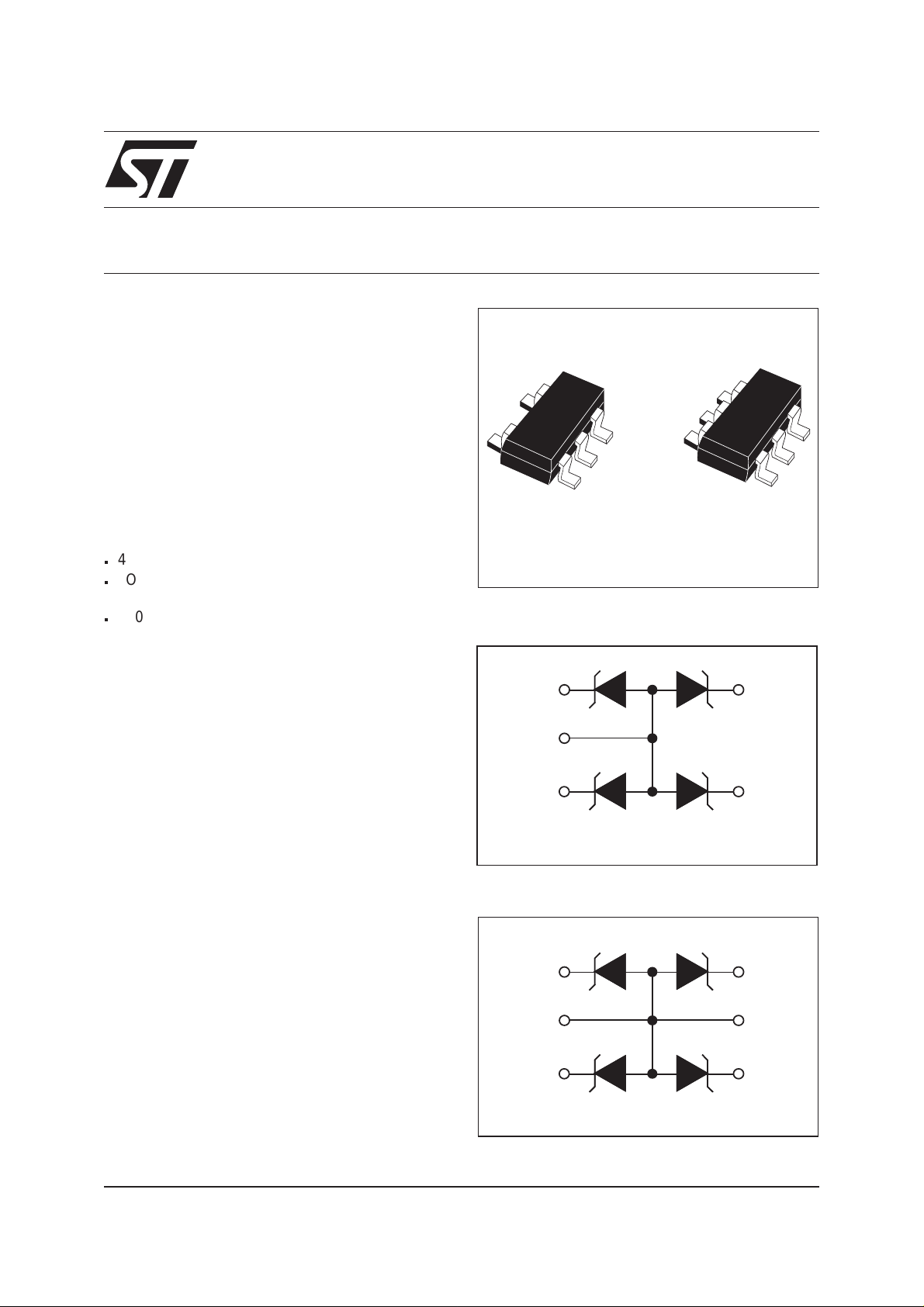
DESCRIPTION
QUAD TRANSIL ARRAY
FOR ESD PROTECTION
SOT23-5L (SC-59)
ESDAxxSC5
FUNCTIONAL DIAGRAM
SOT23-5L
SOT23-6L (SC-59)
ESDAxxSC6
The ESDAxxSC5 and ESDAxxSC6 are monolithic
voltage suppressors designed to protect
components which are connected to data and
transmission lines against ESD.
They clamp the voltage just above the logic level
supply for positive transients, and to a diode drop
below ground for negative transient.
BENEFITS
High ESD protection level : up to 25 kV
High integration
Suitable for high density boards
COMPLIES WITH THE FOLLOWING STANDARDS:
IEC61000-4-2 : level 4
MIL STD 883C-Method 3015-6 : class3
(human body model)
1
2
3
SOT23-6L
1
2
3
5
4
6
5
4
March 2000 Ed: 5D
1/7
ESDAxxSC5 / ESDAxxSC6
ABSOLUTE MAXIMUM RATINGS (T
amb
= 25°C)
Symbol Test conditions Value Unit
V
PP
P
PP
T
j
T
stg
T
L
T
op
note 1: 300 W for ESDA14V2SC5 AND ESDA14V2SC6
note 2: Evolution of functional parameters is given by curves.
ELECTRICAL CHARACTERISTICS (T
Symbol Parameter
V
RM
V
BR
V
CL
I
RM
I
PP
αT
C
Rd
V
F
ESD discharge - MIL STD 883C - Method 3015-6
IEC61000-4-2 air discharge
IEC61000-4-2 contact discharge
Peak pulse power (8/20µs) note1
Junction temperature
Storage temperature range
Lead solder temperature (10 second duration)
Operating temperature range
= 25°C)
amb
Stand-off voltage
Breakdown voltage
V
Clamping voltage
BR
Leakage current
Peak pulse current
Voltage temperature coefficient
Capacitance
Dynamic resistance
Slope:
Forward voltage drop
25
16
9
500 W
150 °C
-55 to +150 °C
260 °C
-40 to +125 °C
I
I
F
I
I
RM
PP
V
F
V
RM
1
Rd
kV
V
@IRIRM@V
V
BR
min. max. max. typ. max. typ. max.
Types
VVmAµAVmΩ10
ESDA5V3SC5
5.3 5.9 1 2 3 230 5 280 1.25 200
ESDA5V3SC6
ESDA6V1SC5
6.1 7.2 1 20 5.25 350 6 190 1.25 200
ESDA6V1SC6
ESDA14V2SC5
14.2 15.8 1 5 12 650 10 100 1.25 200
ESDA14V2SC6
ESDA25SC6
note 1 : Square pulse, Ipp = 15A, tp=2.5µs.
note 2 : ∆ VBR= αT* (Tamb -25°C) * VBR(25°C)
2/7
25 30 1 1 24 1000 10 60 1.2 10
Rd αTCV
RM
note 1 note 2 0V bias
-4
/°C pF V mA
@I
F
F

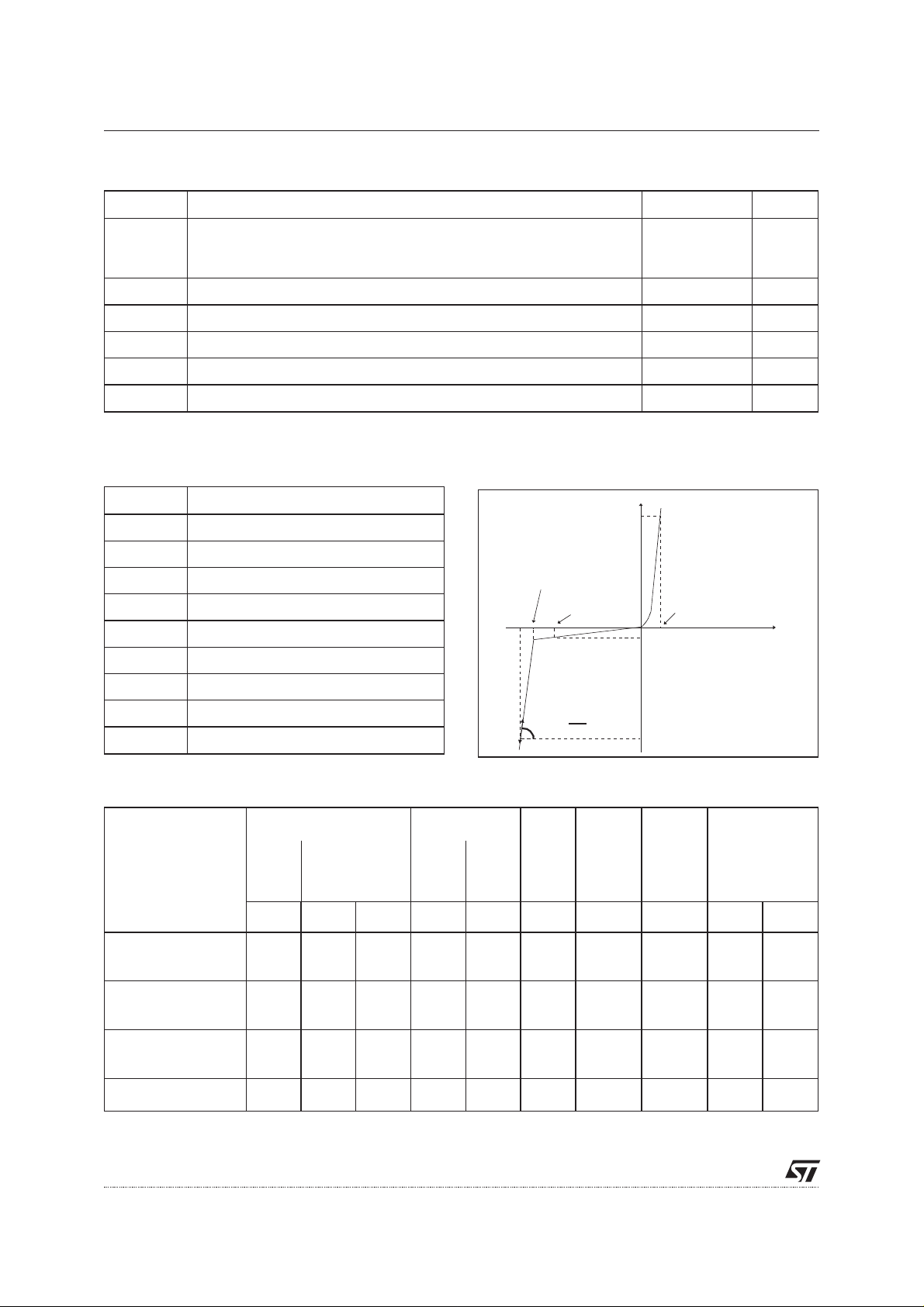
CALCULATION OF THE CLAMPING VOLTAGE
USE OF THE DYNAMIC RESISTANCE
The ESDA familyhasbeendesigned to clamp fast
spikes like ESD. Generally the PCB designers
need to calculate easily the clamping voltage V
CL
This is why we give the dynamic resistance in
addition to the classical parameters. The voltage
across the protection cell can be calculated with
the following formula:
VCL=VBR+RdI
PP
WhereIppisthepeak currentthrough theESDA cell.
DYNAMIC RESISTANCE MEASUREMENT
The short duration of the ESDhasledusto prefer
amoreadapted testwave, as belowdefined, tothe
classical 8/20µs and 10/1000µs surges.
I
Ipp
ESDAxxSC5 / ESDAxxSC6
As the value of the dynamic resistance remains
stable for a surge duration lower than 20µs, the
.
2.5µs rectangular surge is well adapted. In
addition both rise and fall times are optimized to
avoid any parasitic phenomenon during the
measurement of Rd.
2µs
tp = 2.5µs
2.5µs duration measurement wave.
t
3/7

ESDAxxSC5 / ESDAxxSC6
Fig. 1: Peak power dissipation versus initial
junction temperature.
Ppp[Tj initial]/Pp p [T j in itia l= 2 5 °C]
1.1
1.0
0.9
0.8
0.7
0.6
0.5
0.4
0.3
0.2
0.1
0.0
0 25 50 75 100 125 150
Tj initial(°C)
Fig. 3: Clamping voltage versus peak pulse
current (Tj initial = 25 °C).
Rectangular waveform tp = 2.5 µs.
Ipp(A)
50.0
10.0
ESDA6V1SC5/SC6
1.0
ESDA5V3SC5/SC6
Vcl(V)
0.1
0 5 10 15 20 25 30 35 40 45 50 55 60 65 70 75 80
ESDA25SC5/SC6
ESDA14V2SC5/SC6
tp=2.5µs
Fig. 2:Peak pulsepowerversus exponentialpulse
duration (Tj initial = 25 °C).
Ppp(W)
5000
ESDA5V3SC5/SC6
&
1000
ESDA14V2SC5/SC6
&
ESDA25SC6
ESDA6V1SC5/SC6
tp(µs)
100
1 10 100
Fig. 4: Capacitance versus reverse applied
voltage (typical values).
C(pF)
500
200
100
50
ESDA5V3SC5/SC6
ESDA6V1SC5/SC6
ESDA14V2SC5/SC6
20
VR(V)
10
12 51020 50
F=1MHz
Vosc=30mV
ESDA25SC6
Fig. 5:Relative variation ofleakage current versus
junction temperature (typical values).
IR[Tj] / IR[Tj=25°C ]
200
Tj(°C)
ESDA14V2SC5/SC6
&
ESDA6V1SC5/SC6
ESDA25SC6
ESDA5V3SC5/SC6
100
10
1
25 50 75 100 125
4/7
Fig. 6: Peak forward voltage drop versus peak
forward current (typical values).
IFM(A)
5.00
ESDA5V3SC5/SC6
1.00
0.10
0.01
0.5 1.0 1.5 2.0 2.5 3.0 3.5 4.0
ESDA14V2SC5/SC6
ESDA6V1SC5/SC6
VFM(V)
&
ESDA25SC6
Tj=25°C

ESD protection by ESDAXXXSCX
ESDAxxSC5 / ESDAxxSC6
Electrostatic discharge (ESD) is a major cause of
failure in electronic systems.
Transient Voltage Suppressors (TVS) are an ideal
choice for ESD protection. They are capable of
clamping the incoming transient overvoltage to a
low enough level such that damage to the
protected semiconductor is prevented.
SurfacemountTVS arraysofferthe bestchoicefor
minimal lead inductance.
I/ O LINES
They serve as parallel protection elements,
connected between the signal line and ground. As
the transient rises above the operating voltage of
the device, the TVS array becomes a low
impedance path diverting the transient current to
ground.
ESD
sensitive
device
ESDA6V1SC6 (1connection to GND for ESDAxxSC5)
The ESDAxxSCx array is the ideal board level
protection of ESD sensitive semiconductor
components.
ThetinySOT23-5L andSOT23-6L packages allow
design flexibility in the high density boards where
the space saving is at a premium. This enables to
shorten the routing and contributes to hardening
against ESD.
ADVICE FOR OPTIMIZING CIRCUIT BOARD
LAYOUT
Circuit board layout is a critical design step in the
suppression of ESD induced transients. The
following guidelines are recommended :
n
TheESDAxxSC5/6should beplaced ascloseas
possible to the input terminals or connectors.
GND
n
The path length between the ESD suppressor
and the protected line should be minimized
n
All conductive loops, including power and
ground loops should be minimized
n
The ESD transient return path to ground should
be kept as short as possible.
n
Ground planes should be used whenever possible.
5/7

ESDAxxSC5 / ESDAxxSC6
ORDER CODE
ESDA 6V1 SC6
ESD ARRAY
MARKING
Type Marking
ESDA6V1SC5 EC61
ESDA6V1SC6 ES61
ESDA5V3SC5 EC53
Packaging: Standard packaging is tape and reel.
PACKAGE MECHANICAL DATA
SOT23-5L
A
H
e
D
e
b
A2
V
BR min
PACKAGE :
SC5: SOT23-5L
SC6: SOT23-6L
MARKING
Type Marking
ESDA5V3SC6 ES53
ESDA14V2SC5 EC15
ESDA14V2SC6 ES15
ESDA25SC6 ES25
Packaging: Standard packaging is tape and reel.
DIMENSIONS
REF.
Millimeters Inches
Min. Typ. Max. Min. Typ. Max.
A 0.90 1.45 0.035 0.057
A1 0 0.15 0 0.006
A2 0.90 1.30 0.035 0.0512
FOOT PRINT
1
3.6
0.137
6/7
0.040
A1
L
c
M
E
b 0.35 0.50 0.0137 0.02
c 0.09 0.20 0.004 0.008
D 2.80 3.00 0.11 0.118
E 1.50 1.75 0.059 0.0689
e 0.95 0.0374
H 2.60 3.00 0.102 0.118
0.65
0.025
0.95
0.037
1.3
0.051
mm
inch
L 0.10 0.60 0.004 0.024
M 10° 10°

PACKAGE MECHANICAL DATA
SOT23-6L
H
A
A2
REF.
ESDAxxSC5 / ESDAxxSC6
DIMENSIONS
Millimeters Inches
e
D
e
FOOT PRINT
1
3.6
0.137
0.040
Min. Typ. Max. Min. Typ. Max.
b
A 0.90 1.45 0.035 0.057
A1 0 0.15 0 0.006
A2 0.90 1.30 0.035 0.0512
A1
L
c
M
E
b 0.35 0.50 0.0137 0.02
C 0.09 0.20 0.004 0.008
D 2.80 3.00 0.11 0.118
E 1.50 1.75 0.059 0.0689
e 0.95 0.0374
H 2.60 3.00 0.102 0.118
L 0.10 0.60 0.004 0.024
0.65
0.025
1.3
0.051
mm
inch
M 10° 10°
0.95
0.037
Informationfurnished is believedto be accurateandreliable. However, STMicroelectronicsassumesno responsibility fortheconsequences of
useof such informationnor for anyinfringementof patents orotherrights of thirdpartieswhich may resultfromits use. Nolicense is grantedby
implication or otherwise under any patent or patent rights of STMicroelectronics. Specifications mentioned in this publication are subject to
change without notice. This publication supersedes and replaces all information previously supplied.
STMicroelectronics products are not authorizedfor use as critical components in life support devices or systems without express writtenapproval of STMicroelectronics.
The ST logo is a registered trademark of STMicroelectronics
© 2000 STMicroelectronics - Printed in Italy - All rights reserved.
STMicroelectronics GROUP OF COMPANIES
Australia - Brazil- China - Finland - France- Germany - Hong Kong- India - Italy - Japan- Malaysia
Malta - Morocco- Singapore - Spain - Sweden- Switzerland - United Kingdom- U.S.A.
http://www.st.com
7/7
 Loading...