

ESDA25DB3
ApplicationSpecific Discretes
A.S.D.
APPLICATIONS
Where transient overvoltage protection in esd
sensitiveequipmentisrequired,such as :
-COMPUTERS
-PRINTERS
-COMMUNICATIONSYSTEMS
It is particulary recommended for RS232 I/O port
protectionwherethe lineinterfacewithstands2kV,
ESDsurges.
FEATURES
18BIDIRECTIONALTRANSILFUNCTIONS
LOWCAPACITANCE:C=30pF@V
500 W peak pulsepower(8/20µs)
DESCRIPTION
The ESDA25DB3 is a dual monolithic voltage
suppressordesignedto protect componentswhich
are connected to data and transmission lines
againstESD.
BENEFITS
HighESDprotection level: up to 25kV
Highintegration
Suitablefor high density boards
COMPLIESWITHTH EFOLLOWINGSTA NDAR DS:
IEC1000-4-2: level4
MILSTD883C-Method3015-6: class3
(humanbody model)
RM
TRANSILARRAY
FOR ESD PROTECTION
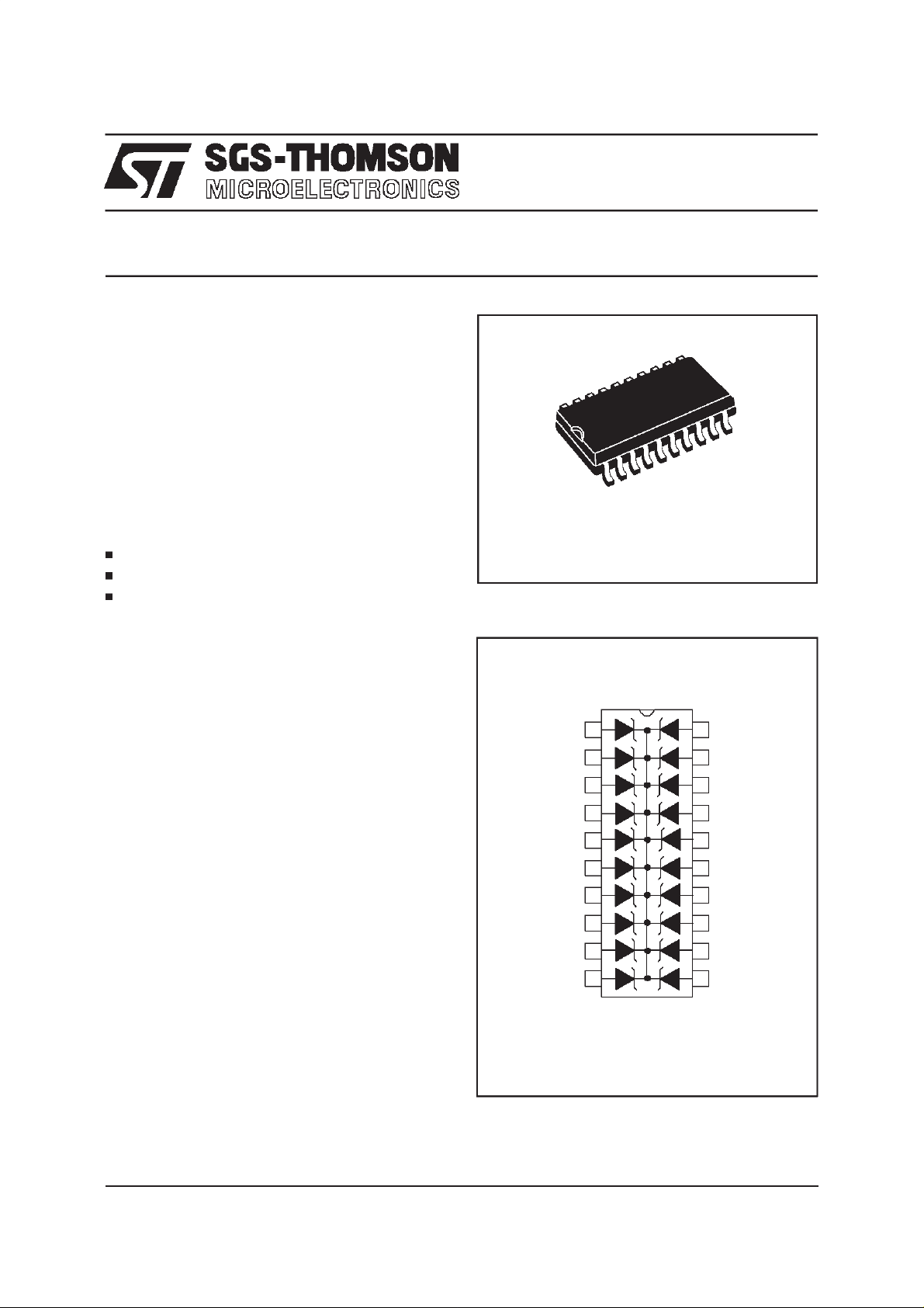
SO20
FUNCTIONAL DIAGRAM
I/O1
I/O2
I/O3
I/O4
I/O5
I/O6
I/O7
I/O8
I/O9
GND GND
1
2
3
4
5
6
7
8
9
10
20
19
18
17
16
15
14
13
12
11
I/O 18
I/O 17
I/O 16
I/O 15
I/O 14
I/O 13
I/O 12
I/O 11
I/O 10
January 1998 - Ed : 2
1/5
ESDA25DB3
ABSOLUTEMAXIMUMRATINGS(T
amb
=25°C)
Symbol Parameter Value Unit
V
PP
Electrostaticdischarge
25 kV
MILSTD883C- Method3015-6
P
PP
T
stg
T
j
T
L
ELECTRICALCHARACTERISTICS
Peakpulse power(8/20µs) 500 W
Storagetemperaturerange
Maximumjunction temperature
- 55 to +150
125
Maximumlead temperatureforsolderingduring 10s 260
=25°C)
(T
amb
Symbol Parameter
V
RM
V
BR
V
CL
I
RM
Stand-offvoltage
Breakdownvoltage
Clampingvoltage
Leakagecurrent
°C
°C
°
C
I
PP
α
T Voltagetemperaturecoefficient
Peak pulsecurrent
C Capacitance
Rd Dynamicresistance
Types V
@ I
BR
R
I
RM
@V
RM
Rd αTC
min. max. max. typ. max. typ.
note1 note1 note2 note 3 0Vbias
VVmA
µ
AV
Ω
-4
10
/°CpF
ESDA25DB3 25 30 1 2 24 0.5 9.7 50
note 1 : Betwennany I/O pin Groung
note 2 : Squarepulse, Ipp = 25A, tp=2.5µs.
note 3 : ∆ V
=αT* (Tamb-25°C)* VBR(25°C)
BR
2/5

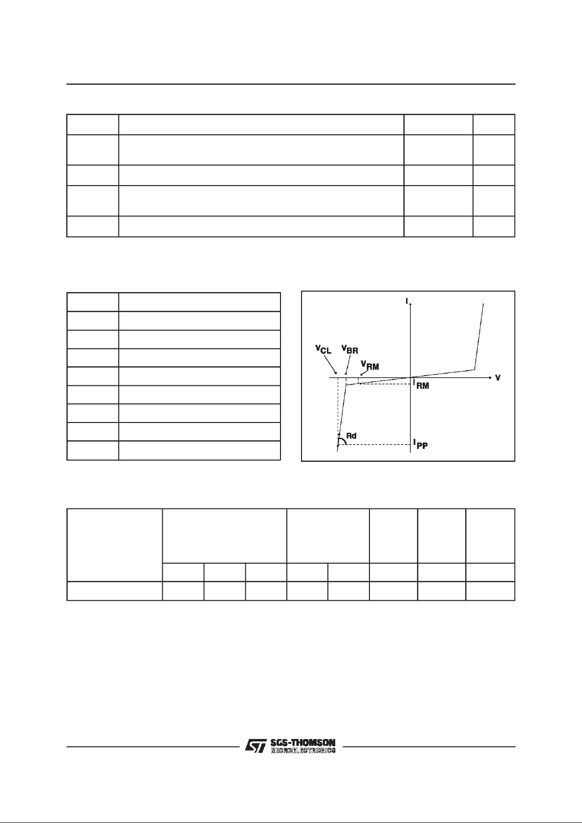
CALCULATION OF THECLAMPING VOLTAGE
USEOFTHEDYNAMIC RESISTANCE
TheESDAfamilyhasbeen designed to clamp fast
spikes like ESD. Generally the PCB designers
need to calculate easily the clampingvoltageV
CL
This is why we give the dynamic resistance in
addition to the classical parameters. The voltage
across the protection cell can be calculated with
thefollowingformula:
V
CL=VBR
+RdI
PP
WhereIppisthepeakcurrentthroughtheESDAcell.
DYNAMICRESISTANCEMEASUREMENT
Theshortdurationof theESDhas led ustoprefer
amoreadaptedtestwave,as belowdefined,to the
classical8/20µs and 10/1000µssurges.
I
Ipp
ESDA25DB3
As the value of the dynamic resistance remains
stable for a surge duration lower than 20µs, the
.
2.5µsrectangularsurgeis welladapted. Inaddition
bothrise and fall times are optimizedto avoid any
parasiticphenomenonduringthe measurementof
Rd.
2µs
tp = 2.5µs
2.5µsdurationmeasurementwave.
t
3/5

ESDA25DB3
Fig. 1 :
Peak power dissipation versus initial
junctiontempearature.
Ppp[Tj initial]/Ppp[Tjinitial=25°C]
1.1
1.0
0.9
0.8
0.7
0.6
0.5
0.4
0.3
0.2
0.1
0.0
0 25 50 75 100 125 150
Fig. 3 :
Clamping voltage versus peak pulse
Tj initial(°C)
current(Tj initial=25 °C).
Rectangularwaveformtp = 2.5µs.
Ipp(A)
50.0
10.0
tp=2.5µs
Fig. 2 :
Peak pulse power versus exponential
pulseduration(Tj initial= 25 °C).
Ppp(W)
5000
1000
tp(µs)
100
1 10 100
Fig. 4 : Capacitance versus reverse applied
voltage(typicalvalues).
C(pF)
100
F=1MHz
Vosc=30mV
50
1.0
0.1
20 25 30 35 40 45 50 55 60
V (V)CL
Fig.5 : Relativevariationof leakagecurrentversus
junctiontemperature(typical values).
I [Tj] / I [Tj=25°C]
RR
200
100
10
Tj(°C)
1
25 50 75 100 125
20
V (V)R
10
12 510 30
4/5

ORDERCODE
ESDARRAY
ESDA25DB3
ESDA 25 D B 3 RL
PACKAGING:
RL = Tape andreel
= Tube
Package:SO20
VBRmin
MARKING : Logo,Date Code, E25DB3
PACKAGEMECHANICALDATA
SO20 Plastic
D
A
K
e
A1B
EH
L
hx45°
Bidirectionel
DIMENSIONS
REF.
Millimetres Inches
Min. Typ. Max. Min. Typ. Max.
A 2.65 0.104
C
A1 0.10 0.20 0.004 0.008
B 0.33 0.51 0.013 0.020
C 0.23 0.32 0.009 0.013
D 12.6 13.0 0.484 0.512
E 7.40 7.60 0.291 0.299
e 1.27 0.050
H 10.0 10.65 0.394 0.419
h 0.50 0.020
L 0.50 1.27 0.020 0.050
K8°(max)
Packaging :
Weight:
Information furnished is believed to be accurate and reliable. However, SGS-THOMSON Microelectronics assumes no responsibility for the
consequences of use of such information nor for any infringementof patents or other rights of third parties which may result from its use. No
license is grantedby implication or otherwiseunder any patent orpatent rightsof SGS-THOMSON Microelectronics.Specifications mentioned
in thispublication are subject tochange withoutnotice. This publicationsupersedes and replaces all information previously supplied.
SGS-THOMSONMicroelectronics productsare not authorizedfor use ascriticalcomponents inlife support devices or systems without express
written approval of SGS-THOMSONMicroelectronics.
Australia - Brazil - Canada- China - France- Germany - Italy- Japan - Korea- Malaysia- Malta- Morocco
The Netherlands - Singapore - Spain - Sweden- Switzerland - Taiwan - Thailand - UnitedKingdom - U.S.A.
Preferredpackaging istapeandreel.
0.55g.
1998SGS-THOMSON Microelectronics- Printed in Italy - All rights reserved.
SGS-THOMSON Microelectronics GROUP OF COMPANIES
5/5
 Loading...