®
ESDA17/19-5SC6
Application Specific Discretes
A.S.D.™
APPLICATIONS
Where transient overvoltage protection in ESD
sensitive equipment is required, such as :
Computers
■
Printers and other peripherals
■
Communications systems
■
Cellular phone handsets and accessories
■
Other telephone sets
■
Consumer Electronics (Set top boxes, DVD
■
players, TV sets)
DESCRIPTION
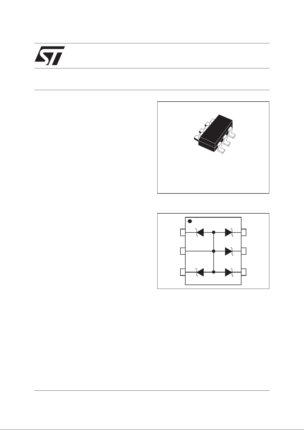
The ESDA17/19-5SC6 is a monolithic array
designed to protect up to 5 lines against ESD
transients.
The device is ideal for applications where board
space savind is required.
TRANSIL™ ARRAY
FOR ESD PROTECTION
SOT23-6L
ESDAxx-5SC6
FUNCTIONAL DIAGRAM
SOT23-6L
FEATURES
■
5 Unidirectional transil™ functions
■
Minimumbreakdown voltagerange v
BRmin
=17V
or 19V
■
Peak pulse power (8/20µs); 150W
■
Tiny leakage current at stand-off voltage: <
100nA
BENEFITS
■
High ESD protection level
■
High integration
■
Suitable for high density boards
COMPLIES WITH THE FOLLOWING STANDARDS:
- IEC61000-4-2: 15 kV (air discharge)
8 kV (contact discharge)
- MIL STD 883E-Method 3015-7: class3
25kV (human body model)
I/O1
Gnd
I/O2
I/O5
I/O4
I/O3
November 2002 -Ed: 1A
1/5

ESDA17/19-5SC6
ABSOLUTE MAXIMUM RATINGS (T
amb
= 25°C)
Symbol Test conditions Value Unit
V
PP
P
PP
ESD discharge - IEC61000-4-2 air discharge
IEC61000-4-2 contact discharge
Peak pulse power dissipation (8/20µs)
Tj initial = Tamb
±15
±8
150 W
Note 1
T
j
T
stg
T
L
Junction temperature
Storage temperature range
Maximum lead temperature for soldering during 10s at 5mm for
125 °C
-55 to +150 °C
260 °C
case
T
op
Note 1: For a surge greater than the maximum values, the diode will fail in short-circuit.
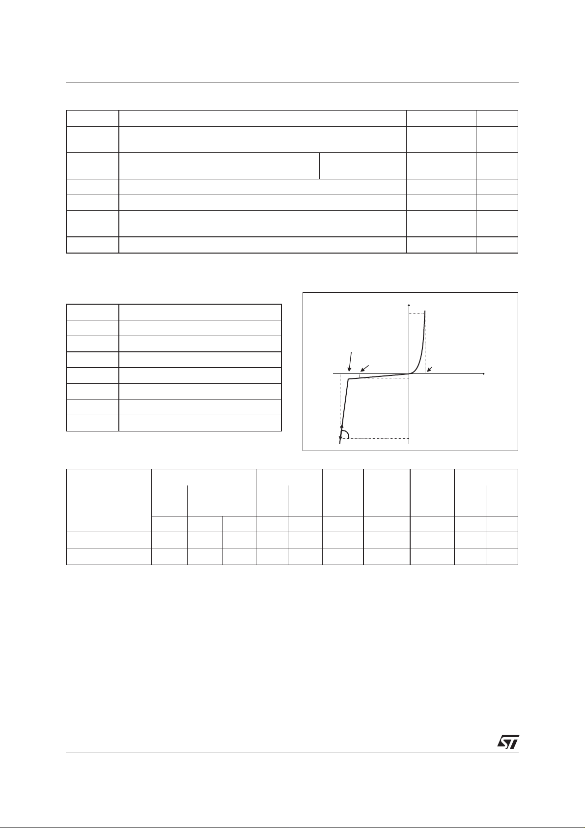
ELECTRICAL CHARACTERISTICS (T
Operating temperature range
= 25°C)
amb
Symbol Parameter
V
V
V
I
RM
I
PP
αT
V
RM
BR
CL
F
Stand-off voltage
Breakdown voltage
Clamping voltage
Leakage current @ V
RM
Peak pulse current
Voltage temperature coefficient
Forward voltage drop
V
CL
V
BR
V
RM
Rd
-40 to +125 °C
I
I
F
VF
I
RM
I
PP
kV
V
V
@IRIRM@V
BR
Type
min. max. max. typ. max.
V V mA nA V Ω 10
ESDA17-5SC6
ESDA19-5SC6
Note 1 : Square pulse, Ipp = 15A, tp=2.5µs.
Note 2: ∆ VBR= αT* (Tamb-25°C) * VBR(25°C)
17 19 1 75 14 1 10 33 1.2 10
19 21 1 100 15 1 8.5 33 1.2 10
RM
Rd αTCV
note 1 note 2 0V bias
-4
/°C pF V mA
F@IF
2/5
 Loading...