

®
ESDA14V2-4BF1
QUAD BIDIRECTIONAL TRANSIL™ ARRAY
A.S.D™
APPLICATIONS
Where transient overvoltage protection in ESD
sensitive equipment is required, such as :
Computers
■
Printers
■
Communication systems and cellular phones
■
Video equipment
■
Thisdevice is particularly adaptedto the protection
of symmetrical signals.
DESCRIPTION
The ESDA14V2-4BF1 is a monolithic array
designed to protect up to 4 lines in a bidirectional
way against ESD transients.
The device is ideal for situations where board
space saving is requested.
FEATURES
■ 4 Bidirectional Transil™ functions
■
ESD Protection: IEC61000-4-2 level 4
■
Stand off voltage: 12 V MIN.
■
Low leakage current < 1 µA
■
50W Peak pulse power ( 8/20 )
FOR ESD PROTECTION
Flip Chip package
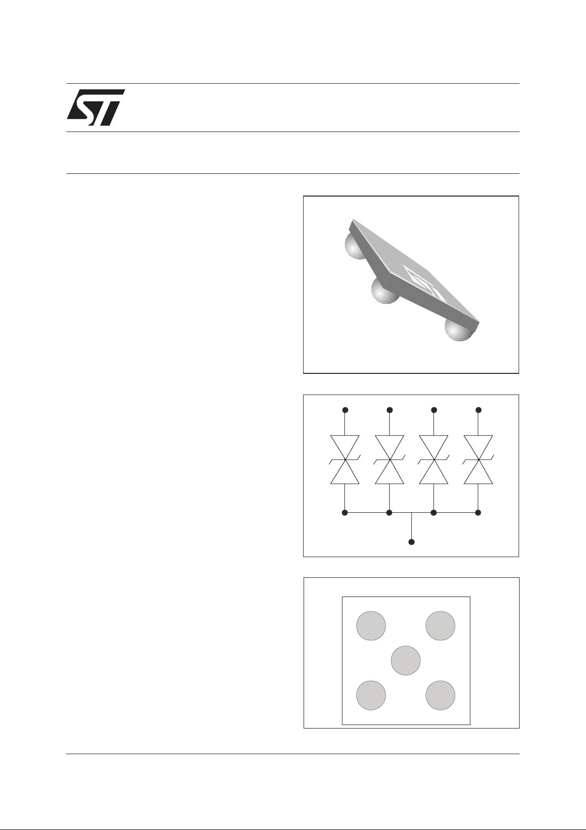
FUNCTIONAL DIAGRAM
A1
A3
C1 C3
BENEFITS
■
High ESD protection level
■
High integration
■
Suitable for high density boards
COMPLIES WITH THE FOLLOWING STANDARDS:
- IEC61000-4-2: 15 kV (air discharge)
8 kV (contact discharge)
- MIL STD 883E-Method 3015-7: class3
25kV (Human Body Model)
July 2002- Ed: 6B
GND
PIN CONFIGURATION (Ball Side)
312
A
B
C
1/9
ESDA14V2-4BF1
ABSOLUTE RATINGS (T
amb
= 25°C)
Symbol Test conditions Value Unit
V
PP
P
PP
T
j
T
stg
T
L
T
op
Note 1: Variation of parameters will be given in the final datasheet
ELECTRICAL CHARACTERISTICS (T
Symbol Parameter
V
RM
V
BR
V
CL
I
RM
ESD discharge - MIL STD 883E - Method 3015-7
IEC61000-4-2 air discharge
IEC61000-4-2 contact discharge
Peak pulse power (8/20µs)
Junction temperature
Storage temperature range
Lead solder temperature (10 seconds duration)
Operating temperature range (note 1)
= 25°C)
amb
Stand-off voltage
Breakdown voltage
Clamping voltage
V
V
CL
Leakage current
BR
±25
±15
±8
50 W
125 °C
-55 to +150 °C
260 °C
-40 to +125 °C
I
V
RM
I
RM
kV
V
I
PP
C
Rd
Peak pulse current
Capacitance
Dynamic resistance
Type
ESDA14V2- 4BF1
Note 1: Square pulse, IPP= 3A, tp = 2.5µs
Note 2: ∆VBR = αT(Tamb-25°C) x VBR(25°C)
V
@I
BR
R
Slope = 1/Rd
IRM@V
RM
I
PP
Rd TC
min. max. max. typ. max. max
note 1 note 2 0V bias
-4
VVmAµAV Ω10
/°C pF
112
14.2 18 1
3.2 10 15
0.1 3
2/9

ESDA14V2-4BF1
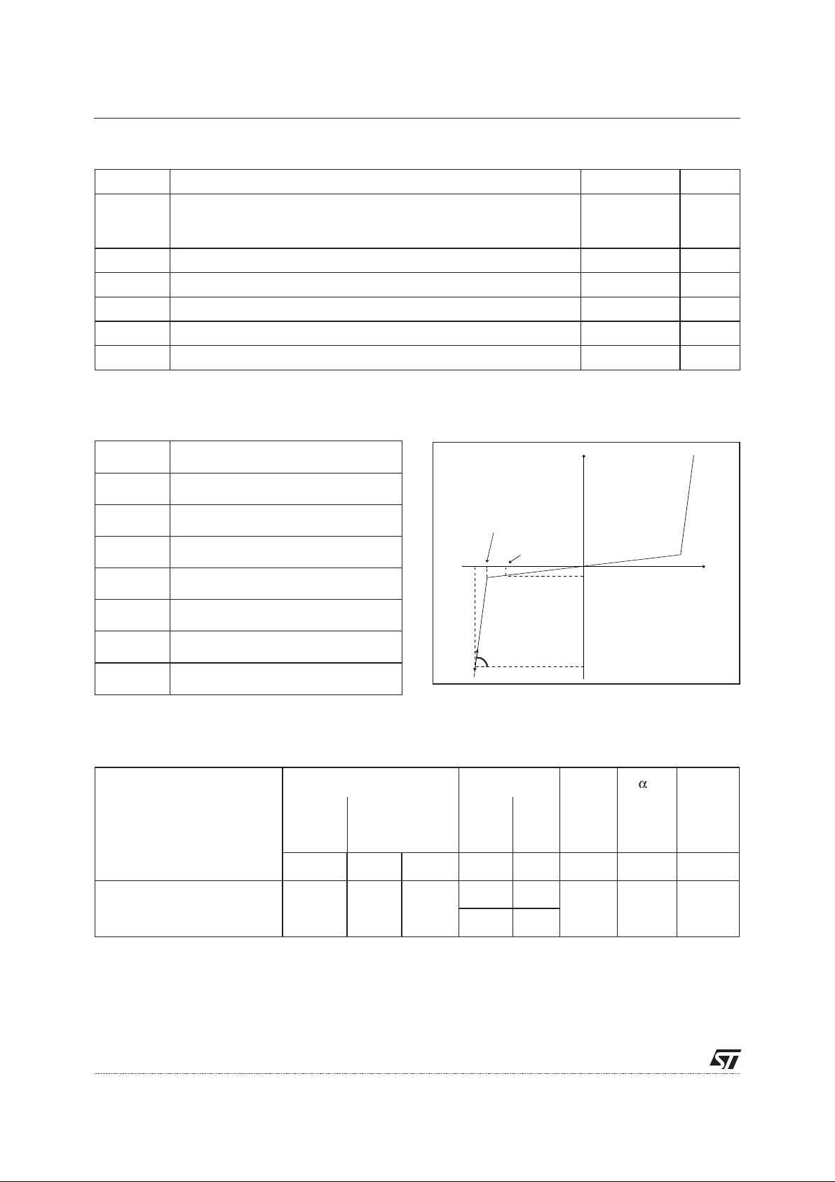
Fig. 1: Clamping voltage versus peak pulse current
(Tjinitial = 25°C) Rectangularwaveformtp = 2.5µs.
Ipp(A)
10.0
tp = 2.5µs
1.0
0.1
0 102030405060
Vcl(V)
Fig. 3: Relative variation of leakage current versus
junction temperature (typical values).
IR[Tj] / IR[Tj=25°C]
1000
100
Fig. 2: Capacitance versus reverse applied voltage
(typical values).
C(pF)
14
12
10
8
6
4
2
0
02468101214
VR(V)
F=1MHz
Vosc=30mV
Tj=25°C
RMS
10
Tj(°C)
1
25 50 75 100 125
APPLICATION EXAMPLE
A1
Connector
A3
C1
B2
C3
IC
to be
protected
3/9

ESDA14V2-4BF1
TECHNICAL INFORMATION
1. ESD protection by ESDA14V2- 4BF1
With the focus of lowering the operation levels, the problem of malfunction caused by the environment is
critical. Electrostatic discharge (ESD) is a major cause of failure in electronic systems.
As a transient voltage suppressor, ESDA14V2-4BF1is an ideal choice for ESD protectionby suppressing
ESDevents. It iscapable of clampingthe incoming transient to a low enough level such that anydamage is
prevented on the device protected by ESDA14V2-4BF1.
ESDA14V2-4BF1serves as a parallel protection elements, connectedbetween the signal line andground.
As the transient rises above the operating voltage of the device, the ESDA14V2-4BF1 becomes a low
impedance path diverting the transient current to ground.
The clamping voltage is given by the following formula:
VVRI
=+.
CL BR d pp
As shown in figure A1, the ESD strikes are clamped by the transient voltage suppressor.
Fig. A1: ESD clamping behavior
Rg
Ip
Rd
Vg
V
V(i/o)
BR
R load
Device
to be
ESD Surge
ESDA14V2-4BF1
Tohave a good approximationof the remaining voltagesat both Vi/o side,we provide the typicaldynamical
resistance value Rd. By taking into account the following hypothesis :
g>Rd
and Rload > R
d
R
we have:
V
Vi o V R
(/ )=+×
Theresults of the calculation done for V
and R
= 3.2 Ω (typ.) give:
d
BR
= 8 kV,Rg= 330 Ω(IEC 61000-4-2 standard), VBR= 14.2 V(min.)
g
g
d
R
g
protected
V(i/o) = 91.8 V
This confirms the very low remaining voltage across the device to be protected. It is also important to note
that in this approximation the parasitic inductance effect was not taken into account. This could be a few
tenths of volts during a few ns at the Vi/o side.
4/9

V(i/o)
ESDA14V2-4BF1
Fig. A2: ESD test board
TEST BOARD
V(i/o)
®
EB14
15
Fig. A3: ESD test configuration
A1, C1, A3 or C3
± 15kV
ESD Air discharge
B2
V(i/o)
The measurements done here after show very clearly (Fig. A4) the high efficiency of the ESD protection:
theclamping voltage V(i/o) becomes veryclose to +V
(positiveway, Fig. A4a) and -VBR(negativeway,
BR
Fig. A4b).
Fig. A4: Remaining voltage during ESD surge
V(i/o)
a: Response in the positive way
V(i/o)
b: Response in the negative way
5/9

ESDA14V2-4BF1
CROSSTALK BEHAVIOR
Fig. A5: Crosstalk phenomenon
R
G1
Line 1
V
G1
R
G2
R
L1
αβ1G1 12G2V+ V
Line 2
V
G2
DRIVERS
R
L2
RECEIVERS
αβ
2G2 21G1V+ V
Thecrosstalk phenomena aredue to the coupling between2 lines. Couplingfactors ( β12or β21 ) increase
when the gap across lines decreases, particularly in silicon dice. In the example above, the expected
signal on load R
the V
signal represents the effect of the crosstalk phenomenon of the line 1 on the line 2. This
G1
is α2VG2, in fact the real voltage at this point has got an extra value β21VG2. This part of
L2
phenomenon has to be taken into account when the drivers impose fast digital data or high frequency
analog signals. The perturbed line will be more affected if it works with low voltage signal or high load
Fig. A6: Analog crosstalk measurements
Connected to the port1
of the Network Analyser
6/9
TEST BOARD
A1
EB14
15
C3
Connected to the port2
of the Network Analyser

ESDA14V2-4BF1
Fig. A7: Typical analog crosstalk measurements
Typical crosstalk response of ESDA14V2-4BF1 (A1/A3 line)
0.00
-10.00
-20.00
-30.00
-40.00
-50.00
-60.00
-70.00
-80.00
-90.00
-100.0
100.0k 1.0M 10.0M 100.0M 1.0G
FigureA6 gives the measurement circuit for theanalog crosstalk application. In figureA7, the curve shows
theeffect of theline A1 on theline A3. Inusual frequency rangeof analog signals (upto 100MHz) theeffect
on disturbed line is less than -30dB.
f/Hz
Fig. A8: Digital crosstalk measurements configu-
Fig. A9: Digital crosstalk results
ration.
0 - 3V
Pulse generator
f = 5MHz
risetime = 3ns
A1
G1
V
C3
unloaded
B2 = GND
β
21 G1V
unloaded
VG1
β21 G1V
rise time: t = 3ns
crosstalk
10-90%
Figure A8 shows the measurement circuit used to quantify the crosstalk effect in a classical digital
application.
Figure A9 shows that in sucha condition, the impact on the disturbed line is less than 50 mV peak to peak.
No data disturbance was noted on the concerned line. The measurements performed with falling edges
give an impact within the same range.
7/9

Fig. A10: Aplac model
ESDA14V2-4BF1
1.2pF
100m
D02_r
BV = 16
IBV = 1m
CJO = 200p
M = 0.3333
RS = 1
VJ = 0.6
TT = 100n
A1
D02_f
BV = 16
IBV = 1m
CJO = 10.4p
M = 0.3333
RS = 2
VJ = 0.6
TT = 100n
1.2pF
100m
B2
50pH
A3
50m
1.2pF
100m
D02_r
B2
160pH
C1
1.8
C3
1.2pF
100m
ORDER CODE
ESD ARRAY
8/9
ESDA 14V2 - 4 B F 1
V min
BR
Nb of lines
Flip Chip
Bidirectional
Pitch & bump
Defined below

ESDA14V2-4BF1
PACKAGE MECHANICAL DATA
DIE SIZE (all dimensions in µm)
700 ± 50
315 ± 50
650 ± 65
MARKING
265
275
diam 230
1270
200
EAT
YWW
1270
OTHER INFORMATION
495 ± 50
1270 ± 50
®
220
40
1270 ± 50
■
YWW: Date code
Ordering code Marking Package Weight Base qty Delivery mode
ESDA14V2-4BF1
EAT Flip-Chip 2.1 mg 5000 Tape& reel 7”
Note: More packing informations are available in the application note AN1235: "Flip-Chip: Package description and recommandations for use"
Informationfurnishedis believed tobeaccurate and reliable. However,STMicroelectronics assumes no responsibilityforthe consequences of
useofsuch information nor foranyinfringement of patents orother rights of thirdpartieswhich may result fromitsuse. No licenseisgranted by
implication or otherwise under any patent or patent rights of STMicroelectronics. Specifications mentioned in this publication are subject to
change without notice. This publication supersedes and replaces all information previously supplied.
STMicroelectronics products are not authorized for use as critical components in life support devices or systems without express written approval of STMicroelectronics.
The ST logo is a registered trademark of STMicroelectronics
© 2002 STMicroelectronics - Printed in Italy - All rights reserved.
STMicroelectronics GROUP OF COMPANIES
Australia - Brazil - Canada - China - Finland - France - Germany
Hong Kong - India - Israel - Italy - Japan - Malaysia - Malta - Morocco - Singapore
Spain - Sweden - Switzerland - United Kingdom - United States.
http://www.st.com
9/9
 Loading...