


EMIF10-COM01
®
January 2002 - Ed: 5A 1/5
Flip Chip package
12345
E
D
C
B
A
02 0403 05
06 0908 01007
GNDGND GND
I1
I9I8 I10
I2 I4
I3 I5
GNDGND
I6
I7
01
PIN CONFIGURATION (Ball Side)
EMI FILTER
INCLUDING ESD PROTECTION
IPAD.
TM
The EMIF10-COM01 is a highly integrated device
designed to suppress EMI / RFI noise in all
systems subjected to electromagnetic
interferences. The EMIF10 flip-chip packaging
means the package size is equal to the die size.
That'swhyEMIF10-COM01is avery smalldevice.
Additionally, this filter includes an ESD protection
circuitry which prevents the protected device from
destruction when subjected to ESD surges up to
DESCRIPTION
ASD is a trademark of STMicroelectronics.
Where EMI filtering in ESD sensitive equipment is
required:
■
Computers and printers
■
Communication systems
■
Mobile phones
MAIN APPLICATIONS
■ EMI symetrical (I/O) low-pass filter
■ Very low PCB space consuming:
2.64 x 2.64 mm
2
■ Very thin package: 0.63 mm
■
High efficiencyinESD suppression on both input
& outputPINS(IEC61000-4-2 level 4).
■
High reliability offered by monolithic integration
BENEFITS
Output
Low-pass Filter
R = 200
Cinput = 45 pF
I/O
Ω
Input
BASIC CELL CONFIGURATION
IEC61000-4-2 level 4 15 KV (air discharge)
8 kV (contact discharge)
COMPLIES WITH FOLLOWING STANDARD:
EMIF10-COM01
2/5
1.0M 3.0M 10.0M 30.0M 100.0M 300.0M 1.0G 3.0G
-50.00
-45.00
-40.00
-35.00
-30.00
-25.00
-20.00
-15.00
-10.00
-5.00
0.00
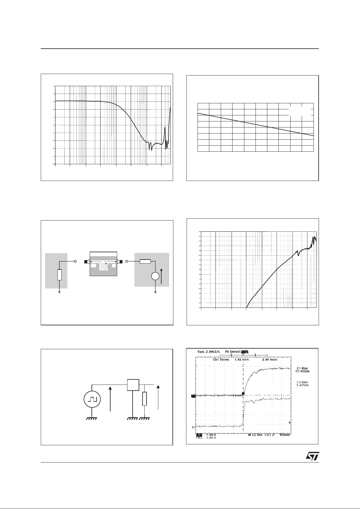
EMIF10-COM01:Typical S21(dB) measurement on line I10/O10
dB
f/Hz
Filtering Behavior
Vout
Vin
Rise Time
1.0M 3.0M 10.0M 30.0M 100.0M 300.0M 1.0G 3.0G
-80.00
-75.00
-70.00
-65.00
-60.00
-55.00
-50.00
-45.00
-40.00
-35.00
-30.00
-25.00
-20.00
-15.00
-10.00
-5.00
0.00
dB
f/Hz
EMIF10-COM01:Typical A1/A2 crosstalk measurement
Crosstalk Behavior
TEST BOARD
out2 in1
50
Ω
Vg
50
Ω
EMIF10
COM01
Analog Crosstalk: Measurements
10
20
30
40
50
012345
VR(V)
C(pF)
F=1MHz
Vosc=30mV
Capacitance versus reverse applied voltage
Note: Spikes at high frequencies are inducedby the PCB layout
EMIF10-COM01
In Out
Square signal
Generator Vc = 2.8V
100k
Vout
Vin
Rise Time: Measurement

EMIF10-COM01
3/5
Symbol Parameters
V
BR
Breakdown voltage
I
RM
Leakage current @ V
RM
V
RM
Stand-off voltage
V
CL
Clamping voltage
R
d
Dynamic impedance
I
PP
Peak pulse current
R
I/O
Series resistance between Input &
Output
C
in
Input capacitance per line
ELECTRICAL CHARACTERISTICS (T
amb
= 25°C)
V
I
V
RM
PP
I
RM
I
V
BR
R
I
V
CL
slope : 1 / Rd
Symbol Parameter and test conditions Value Unit
V
PP
ESD discharge IEC61000-4-2, air discharge
ESD discharge IEC61000-4-2, contact discharg
15
8
kV
T
j
Junction temperature
125 °C
T
op
Operating temperature range
-40 to + 85 °C
T
stg
Storage temperature range
-55 to +150 °C
ABSOLUTE MAXIMUM RATINGS (T
amb
=25°C)
Symbol Test conditions Min Typ Max Unit
V
BR
IR= 1mA
6 8 10 V
I
RM
VRM= 3V per line
500 nA
R
d
IPP= 10A, tp= 2.5µs (see note 1)
1 Ω
R
I/O
180 200 220 Ω
C
in
At 0V bias
45 50 pF
t
LH
Vout = 2.8V Rload = 100kΩ
25 ns

EMIF10-COM01
4/5
EMIF 10 - COM 01
EMI Filter
Nb of lines
For communication
Version
ORDERING CODE
Demif10 model
BV = 7
IBV = 1m
CJO = 25p
M = 0.3333
RS = 1
VJ = 0.6
TT = 100n
out
in
200R
MODEL = demif10 MODEL = demif10
sub
APLAC MODEL
In order to ensure a good efficiency in terms of ESD protection and filtering behavior, we recommend to
implement microvias (100 µm dia.) between the GND bumps and the GND layer. GND bumps can be
connected together inPCBlayer 1, and in addition, if possible,usethrough hole vias (200 um dia.) inboth
sides of filter to improve contact to GND (layer). This layout will minimize the distance to the ground and
thus parasitic inductances. In addition, we recommend to have GND plane wherever possible.
PCB grounding recommendations

EMIF10-COM01
5/5
Informationfurnished is believed to be accurateand reliable. However,STMicroelectronics assumes noresponsibility for the consequencesof
useof such information nor forany infringement ofpatents or otherrights ofthird parties whichmay result fromits use. Nolicense is grantedby
implication or otherwise under any patent or patent rights of STMicroelectronics. Specifications mentioned in this publication are subject to
change without notice. This publication supersedes andreplaces all information previously supplied.
STMicroelectronics products are not authorized for use as critical components in life support devices or systems without express written
approval of STMicroelectronics.
The ST logo is a registered trademark of STMicroelectronics
© 2002 STMicroelectronics - Printed in Italy - All rights reserved.
STMicroelectronics GROUP OF COMPANIES
Australia - Brazil - Canada -China - Finland - France - Germany
Hong Kong - India - Israel - Italy - Japan - Malaysia -Malta - Morocco - Singapore
Spain - Sweden - Switzerland -United Kingdom - United States.
http://www.st.com
2640
2640
500
PACKAGE MECHANICAL DATA
DIE SIZE
2640
300
300
2640
diam 400
®
W
FET
YW
MARKING
650
■
Die size: (2640 ± 50) x (2640 ± 50)
■
Die height (including bumps): 650 ± 65
■
Bump diameter: 315 ± 50
■
Pitch: 500 ± 50
■
Weight: 9.3mg
EMIF10-COM01 is delivered in Tape & Reel (7 inches reel); one Tape & Reel contains 5000 dice.
PACKING:
All dimensions in µm
Note: More packing informationare available in the applicationnote AN1235: "Flip-Chip package descriptionand recommendations for use"
■
Y W W: Date code
 Loading...