


SGS Thomson Microelectronics EMIF09-02726S6, EMIF09-02726S3 Datasheet
EMIF09-02726Sx
Application Specific Discretes
A.S.D.
MAINAPPLICATIONS
Where EMI filtering in ESD sensitive equipmentis
required:
Computersandprinters
Communicationsystems
Mobilephones
MCU Boards
DESCRIPTION
The EMIF09-02726sxis a highly integrated array
designed to suppress EMI / RFI noise in all
systems subjected to electromagnetic
interferences.
Additionally,this filter includes an ESD protection
circuitrywhich prevents the protected device from
destruction when subjected to ESD surges up to
15kV.
BENEFITS
Cost-effectivenesscomparedto discrete
solution
EMI bi-directionallow-passfilter
Highefficiencyin ESD suppression.
Highreliabilityoffered by monolithicintegration
TM
EMI FILTER
INCLUDING ESDPROTECTION
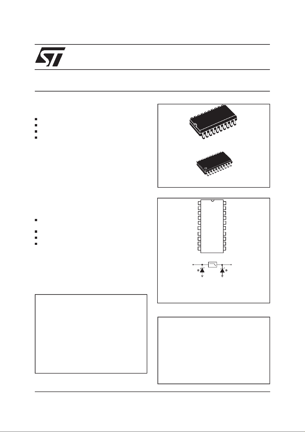
SO-20
SSOP20
PIN-OUTCONFIGURATION
I1
I2
I3
I4
I5
GND GND
I6
I7
I8
I9
9
C
E
L
L
S
O1
O2
O3
O4
O5
O6
O7
O8
O9
COMPLIESWITHTHEFOLLOWINGSTANDARD:
IEC1000-4-2
15kV (airdischarge)
8 kV (contactdischarge)
EMIF09-02726Sxfilteringresponsecurves
ASD is a trademark of STMicroelectronics
August 1999 - Ed: 2
I
DD
R
=27Ω, tolerance +/-20%
I/O
C
=130pF
IN
O
Typicalresponseto IEC1000-4-2
(16kV air discharge)
1/12
EMIF09-02726Sx
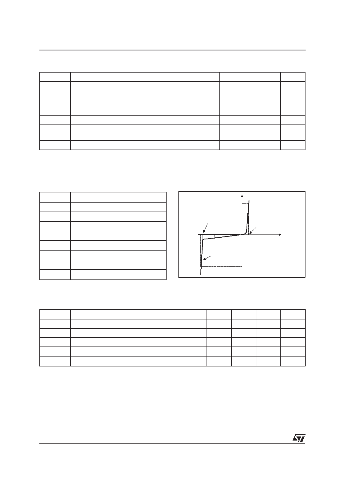
ABSOLUTEMAXIMUM RATINGS
(T
amb
= 25°C)
Symbol Parameter Value Unit
V
PP
Maximumelectrostaticdischargein following
measurementconditions:
MILSTD 883C - METHOD3015-6
IEC1000-4-2- air discharge
IEC1000-4-2- contact discharge
P
PP
T
stg
T
j
T
OP
Peak pulse power (8/20µs) 200 W
Storagetemperaturerange
Junctiontemperature
Operatingtemperaturerange - 40 to+ 85 °C
Symbol Parameter
V
RM
V
BR
V
CL
V
F
C
IN
Stand-offvoltage
Breakdownvoltage
Clampingvoltage
Forwardvoltagedrop
Inputcapacitanceper line
Rd Dynamicimpedance
I
I
RM
PP
Leakagecurrent
Peakpulse current
V
CL
V
BR
V
RM
Slope = 1 / Rd
25
16
9
- 55to +150
150
I
I
F
V
F
I
RM
I
PP
V
kV
°C
°
C
Symbol Testconditions Min. Typ. Max. Unit
I
RM
V
BR
V
F
Rd I
C 0Vbias V
Note 1: VCLcorresponds to the voltage level seen at the output pin
Note 2: Rd is given per diode
Note 3: C is given per diode
2/12
VRM= 5.25V, betweenany I/Opin and GND 20
IR=1 mA, betweenany I/O pin and GND 6.1 7.2 V
IF = 200 mA, betweenanyI/Opin and GND 1.25 V
=15A,tp= 2.5µs (note2) 0.3 Ω
PP
= 30mV F= 1MHz (note3) 130 pF
RMS
µ
A
EMIF09-02726Sx
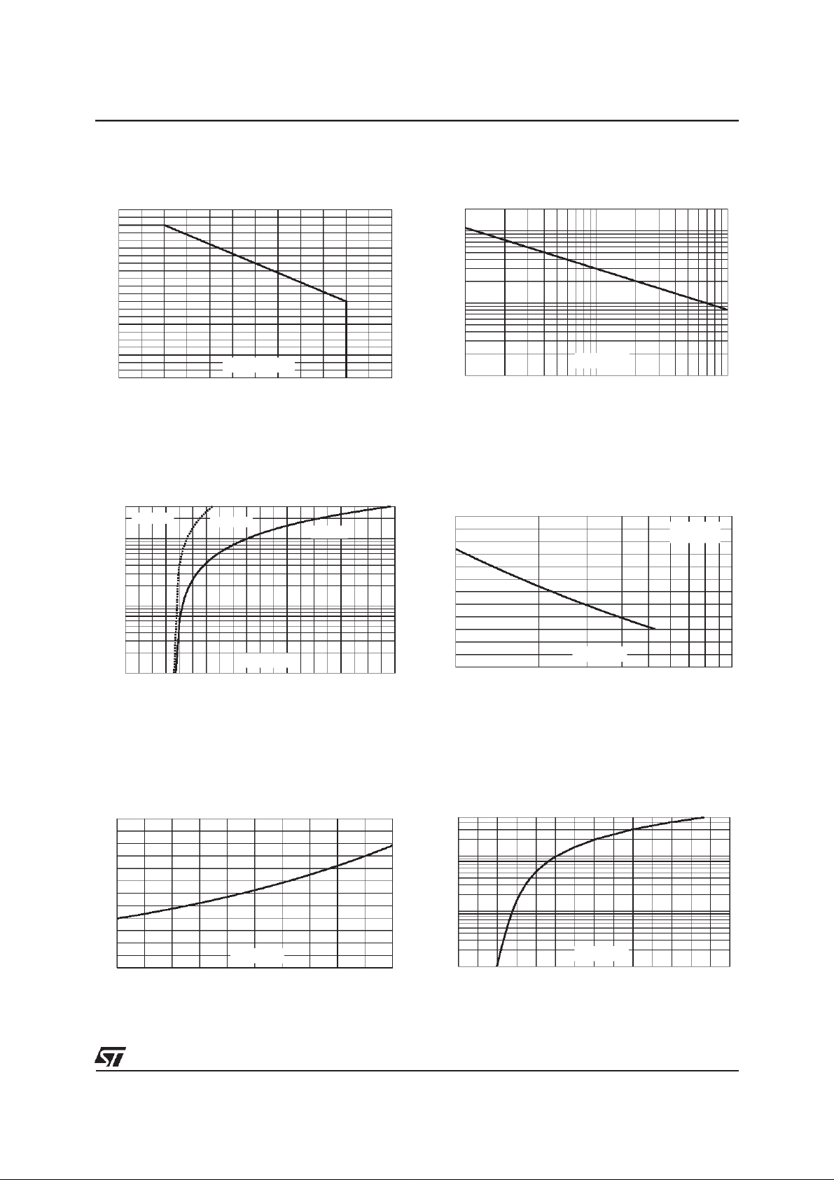
Fig. 1:
Peak power dissipation versus initial junc-
tiontemperature.
Ppp[Tj initial]/Ppp[Tj initial=25°C]
1.1
1.0
0.9
0.8
0.7
0.6
0.5
0.4
0.3
0.2
0.1
0.0
0 25 50 75 100 125 150
Fig. 3:
Clamping voltage versus peak pulse cur-
Tj initial(°C)
rent (Tjinitial=25°C).
Rectangularwaveform: tp= 2.5µs
Ipp(A)
30.0
tp=2.5µs
10.0
Output Vcl
Input Vcl
Fig.2:
Peakpulse powerversusexponentialpulse
duration(Tj initial=25°C).
Ppp(W)
2000
1000
100
tp(µs)
10
1 10 100
Fig. 4:
Input capacitance versus reverse applied
voltage(typicalvalues).
C(pF)
220
200
F=1MHz
Vosc=30mV
1.0
Vcl(V)
0.1
5 6 7 8 9 101112131415
Fig. 5:
Relativevariationof leakagecurrentversus
junctiontemperature(typicalvalues).
IR[Tj] / IR[Tj=25°C]
3.0
2.5
2.0
1.5
1.0
0.5
0.0
25 50 75 100 125 150
Tj(°C)
180
160
140
120
100
12 510
Fig.6:
Peakforwardvoltage drop versuspeak for-
VR(V)
wardcurrent(typicalvalues).
Rectangularwaveform:tp = 2.5µs
IFM(A)
5.00
1.00
0.10
VFM(V)
0.01
0.6 0.8 1.0 1.2 1.4 1.6 1.8 2.0
3/12
EMIF09-02726Sx
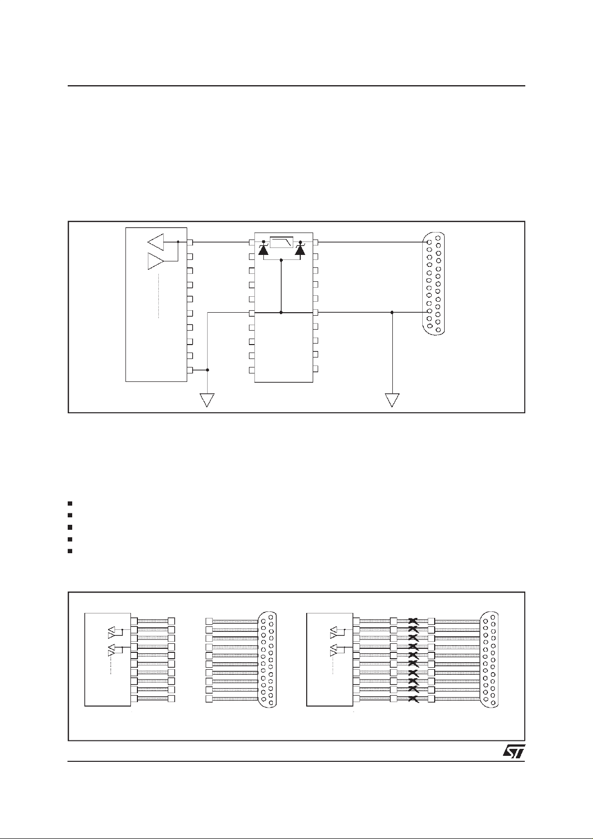
ESDprotectionby the EMIF09-02726Sx
Electrostaticdischarge(ESD)is a major causeof failurein electronicsystems.
TransientVoltage Suppressorsare an ideal choice for ESD protection.They are capableof clamping the
incomingtransientto a lowenoughlevel such that damageto the protectedsemiconductoris prevented.
SurfacemountTVSarrays offer the best choicefor minimallead inductance.
Theyserve as parallel protectionelements, connected betweenthe signal line to ground.As thetransient
risesabove theoperatingvoltageof thedevice,the TVSarraybecomesa lowimpedancepathdivertingthe
transientcurrentto ground.
Fig.7:
Exampleof connectionfor one cell of theEMIF09-02726Sx
I1 O1
O2
O3
O4
Logic
Transceiver
I2
I3
I4
I5 O5
GND GND
I6 O6
I7 O7
EMIF09-02726Sx
I8 O8
I9 O9
1284-A
Connector
The EMIF09-02726Sx array is the ideal board level protection of ESD sensitive semiconductor
components.Itprovidesbestefficiencywhen usingseparatedinputsand outputs, in the socalled4-points
structure.
CircuitBoardLayout
Circuit board layout is a critical design step in the suppressionof ESD induced transients. The following
guidelinesare recommended:
The EMIF09-02726Sxshouldbe placedas near as possible tothe input terminalsor connectors.
The pathlength between theESD suppressorandthe protectedline shouldbe minimized.
Allconductive loops,including powerand groundloops shouldbe minimized.
The ESDtransientreturn path to groundshouldbe keptas short as possible.
Groundplanes should be used wheneverpossible.
Fig.8:
Transceiver,
4/12
RecommendedPCB layout to benefitfrom 4-pointstructure
TO DO
I1
O1
I2
O2
I3
O3
I4
O4
I5
O5
GND
GND
I6
O6
I7
Logic
ASIC,...
EMIF09-02726Sx
O7
I8
O8
I9
O9
footprint
Logic
Transceiver,
ASIC,...
NOT TO DO
I1
O1
I2
O2
I3
O3
I4
O4
I5
O5
GND
GND
I6
O6
I7
O7
I8
O8
I9
O9
EMIF09-02726Sx
footprint