SGS Thomson Microelectronics EMIF01-10005W5 Datasheet

®
EMIF01-10005W5
Application Specific Discretes
A.S.D.
MAIN APPLICATIONS
Where EMI filtering in ESD sensitive equipment is required :
Computers and printers
Communication systems
Mobile phones
MCU Boards
DESCRIPTION
The EMIF01-10005W5 is a highly integrated array
designed to suppress EMI / RFI noise in all systems
subjected to electromagnetic interferen ces.
Additionally, this filter includes an ESD protection circuitry
which prevents the protected device from destruction when
subjected to ESD surges up to 15 kV.
BENEFITS
Cost-effectiveness compared to discrete solution
EMI bi-directional low-pass filter
High efficiency in ESD suppression.
High flexibility in the design of h igh density bo ards
Very low PCB space consuming : 4.2 mm2 typically
High reliability offered by monolithic integration
TM
EMI FILTER
INCLUDING ESD PROTECTION
SOT323-5L
FUNCTIONAL DIAGRAM
I1
GND
I2
O1
O2
COMPLIES WITH THE FOLLOW ING STANDARD:
IEC 1000-4-2 15kV (air discharge)
8 kV (contact discharge)
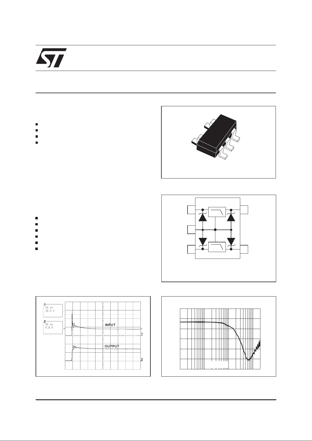
ESD response to IEC1000-4-2 (16 kV air discharge) Filtering response
dB
0
-10
-20
-30
1 10 100 1000 2000
TM
: ASD is trademark of STMicroelectronics.
May 1999 - Ed: 1
R = 100
I/O
C = 50pF
IN
f(MHz)
Ω
1/10

EMIF01-10005W5
= 25 °C)
ABSOLUTE MAXIMUM RATINGS
Symbol Parameter and test conditions Value Unit
(T
amb
V
PP
ESD discharge IEC1000- 4-2, air dis charge
ESD discharge IEC1000- 4-2, c ontact disc harge
T
j
T
op
T
stg
T
L
Junction temperature 150 °C
Operating temperature range -40 to + 85 °C
Storage temperature range -55 to +150 °C
Lead solder temperature (10 second duration) 260 °C
ELECTRICAL CHARACTERISTICS
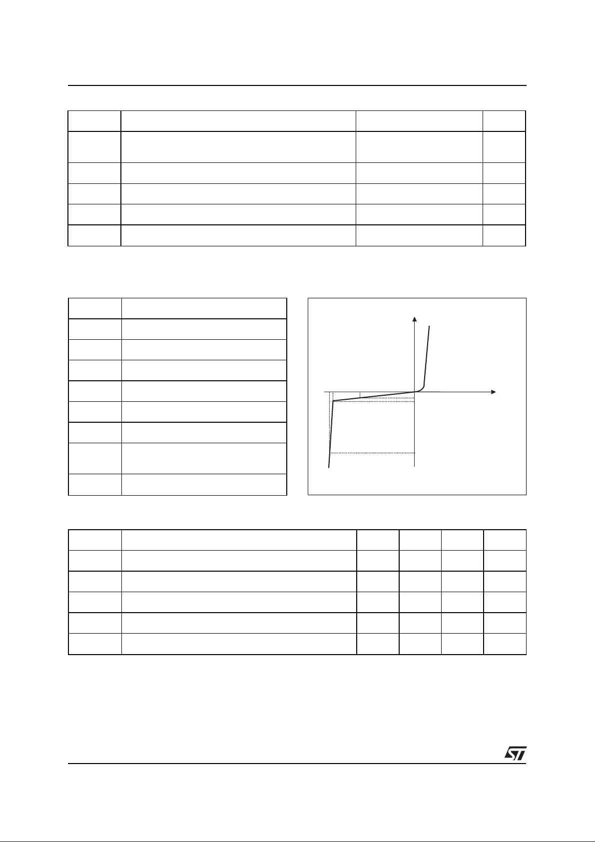
Symbol Parameter
V
BR
I
RM
V
RM
V
CL
Breakdown voltage
Leakage current @ V
Stand-off voltage
Clamping voltage
Rd Dynamic impedance
(T
RM
amb
= 25 °C)
16
kV
9
I
V
V
CL
V
RM
BR
I
RM
I
R
V
I
PP
R
I/O
Peak pulse current
Series resistance between Input
slope : 1 / R
d
I
PP
and Output
C
IN
Input capacitance per line
Symbol Test conditions Min. Typ. Max. Unit
V
I
BR
I
RM
R
I/O
R
d
C
IN
Note 1 : to calculate the ESD residual voltage, please refer to the paragraph "ESD PROTECTION" on pages 4 & 5
= 1 mA 6 7 8 V
R
V
RM
= 3V
1
80 100 120
Ipp = 10 A, tp = 2.5 µs (see note 1) 1
at 0V bias 50 pF
µ
A
Ω
Ω
2/10

EMIF01-10005W5
TECHNICAL INFORMATION
FREQUENCY BEHAV IOR
The EMIF01-10005W5 is firstly designed as an EMI/RFI filter. This low-pass filter is characterized by the following
parameters:
- Cut-off frequency
- Insertion loss
- High frequency rejection
Fig A1:
EMIF01-10005W5 frequency response curve.
dB
0
-10
-20
50Ω
f(MHz)
TG OUT
SMA SMA
TEST BOARD
EMIF01
SPECTRUM ANALYSER
RF IN
50Ω
-30
1 10 100 1000 2000
Figure A1 gives these parameters, in par ticular th e signal re jection at th e GSM frequency is about -24dB at 900 MHz,
Fig A2:
Measurement conditions
TRACKING GENERATOR
Vg
3/10
 Loading...