

HMOS2 SINGLE CHIP SEMI-GRAPHIC
.
SINGLE CHIP LOW-COST COLOR CRT
CONTROLLER
.
TV STANDARDCOMPATIBLE (50Hz or 60Hz)
.
2 SCREENFORMATS :
- 25 (or 21) ROWS OF 40CHARACTERS
- 25 (or 21) ROWS OF 80CHARACTERS
.
ON-CHIP 128 ALPHANUMERIC AND 128
SEMI-GRAPHIC CHARACTER GENERATOR
TWO STANDARD OPTIONS AVAILABLEFOR
ALPHANUMERIC SETS (EF9345-R003IS NO
MOREAVAILABLE)
.
EASY EXTENSION OF USER DEFINED ALPHANUMERIC OR SEMI-GRAPHICSETS
(> 1 K CHARACTERS)
.
40CHARACTERS/ROWATTRIBUTES : FOREGROUNDANDBACKGROUNDCOLOR,DOUBLE HEIGHT, DOUBLE WIDTH, BLINKING,
REVERSE, UNDERLINING, CONCEAL, INSERT, ACCENTUATION OF LOWER CASE
CHARACTERS
.
80 CHARACTERS/ROW ATTRIBUTES : UNDERLINING, BLINKING, REVERSE, COLOR
SELECT
.
PROGRAMMABLE ROLL-UP, ROLL-DOWN
ANDCURSOR DISPLAY
.
ON-CHIPR, G, B, I VIDEOSHIFTREGISTERS
.
EASY SYNCHRONIZATION WITH EXTERNAL VIDEO-SOURCE : ON-CHIP PHASE
COMPARATOR
.
ADDRESS/DATA MULTIPLEXED BUS DIRECTLYCOMPATIBLE WITH STANDARD MICROCOMPUTERS SUCH AS 6801, 6301,
8048,8051, ST9
.
ADDRESSING SPACE : 16K x 8 OF GENERALPURPOSE PRIVATEMEMORY
.
EASY OF USE OF ANY LOW-COST MEMORYCOMPONENTS: ROM, SRAM,DRAM
DESCRIPTION
The EF9345,new advancedcolor CRT controller,
in conjunctionwith an additional standardmemory
packageallowfull implementation of the complete
displaycontrolunit of a color or monochromelowcost termainl, thus significantly reducing IC cost
and PCB space.
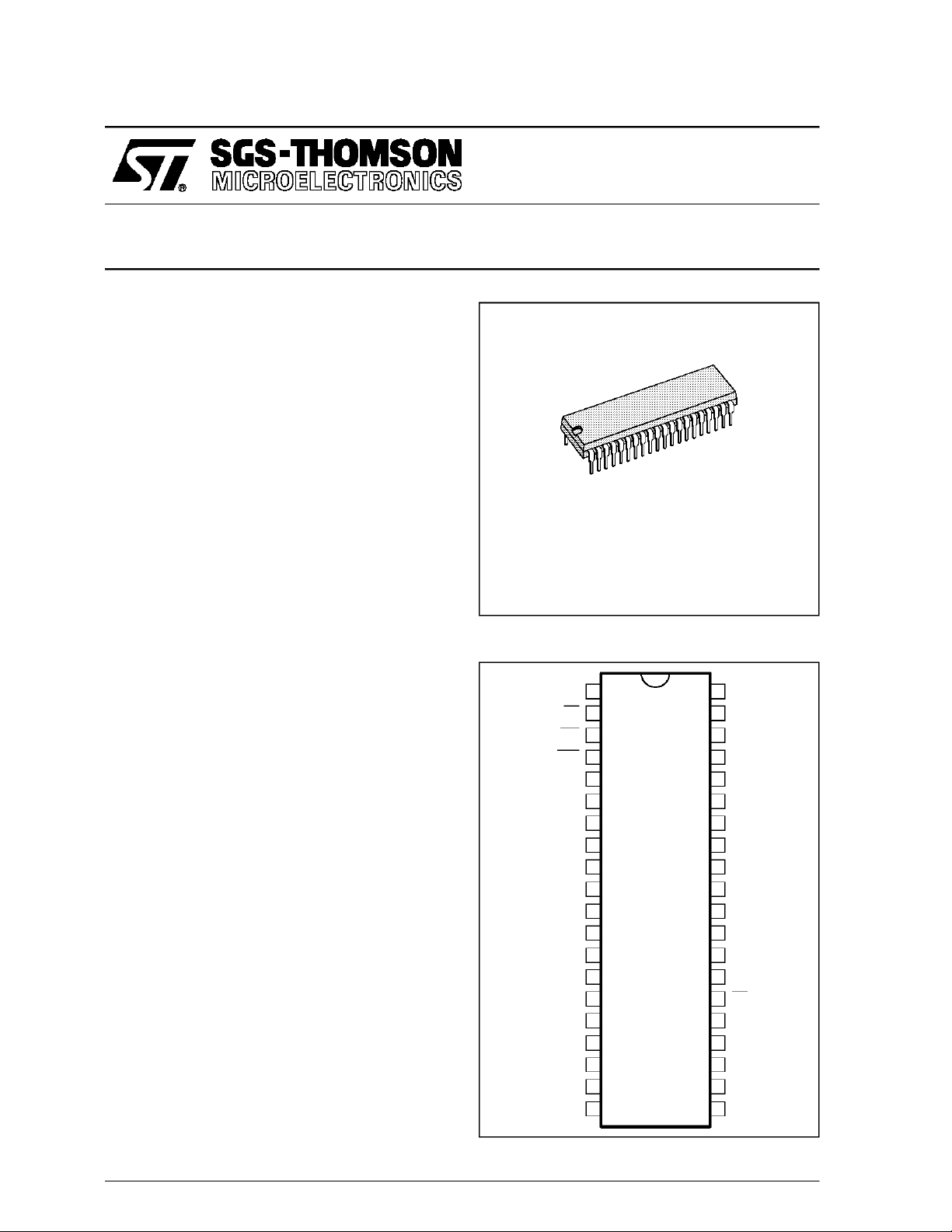
DISPLAY PROCESSOR
(Plastic Package)
ORDER CODE : EF9345P
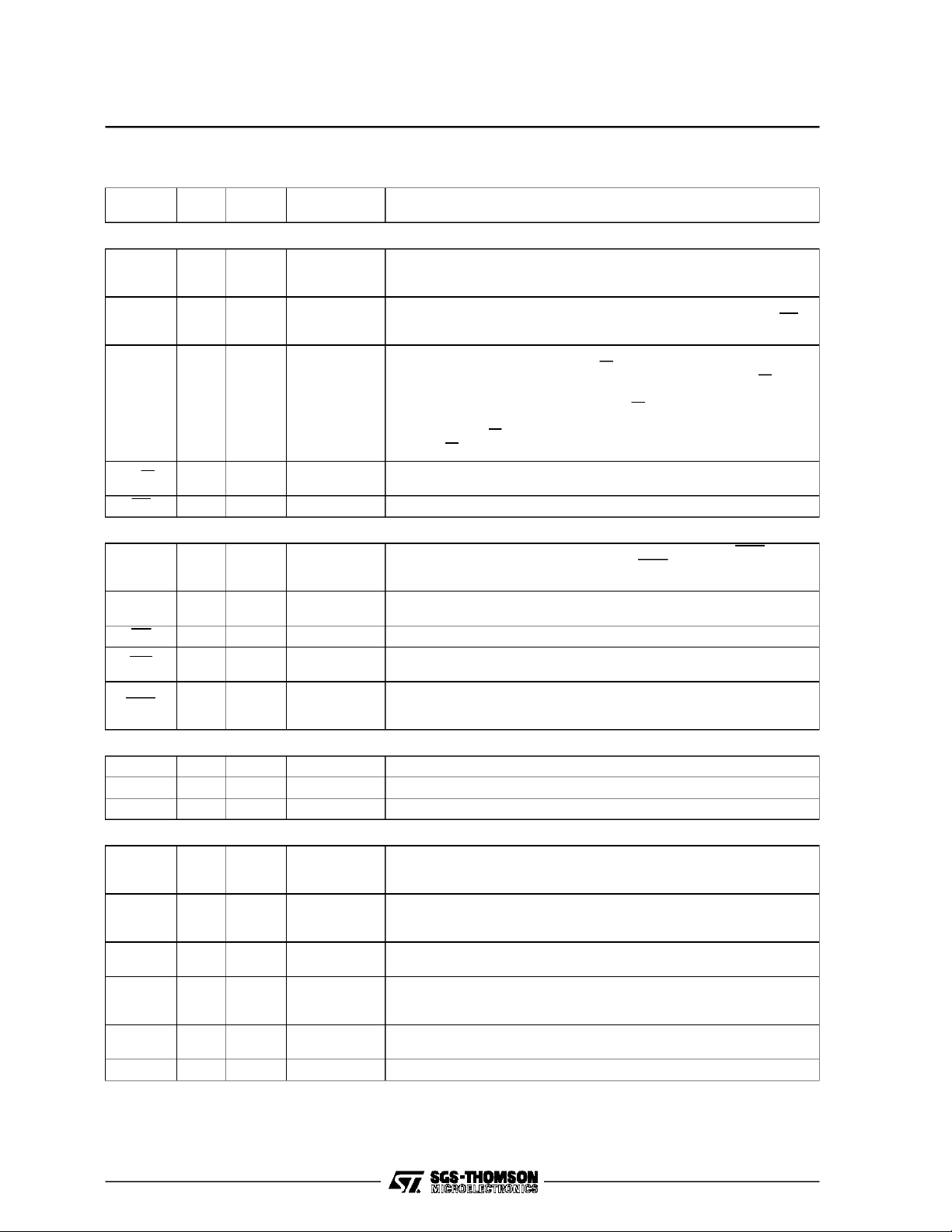
PIN CONNECTIONS
V
ASM
HVS/HS
PC/VS
CLK
SYNC IN
R/W
AD0
AD1
AD2
V
OE
WE
HP
AS
DS
1
SS
2
3
4
5
6
B
7
G
8
R
9
I
10
11
12
13
14
15
16
17
18
19
20
CC
DIP40
EF9345
40
ADM0
39
ADM1
38
ADM2
37
ADM3
36
ADM4
35
ADM5
34
ADM6
33
ADM7
32
AM8
31
AM9
30
AM10
29
AM11
28
AM12
27
AM13
26
CS
25
AD7
24
AD6
23
AD5
22
AD4
21
AD3
9345-01.EPS
March 1995
1/38
EF9345
PIN DESCRIPTION(All the input/outputpins are TTLcompatible)
Name
MICROPROCESSORINTERFACE
AD(0:7) I/O
AS I 14
DS I 15 Data Strobe
R/W I 16 Read/Write
CS I 26 Chip Select The EF9345 is selected when this inputis strobed low by AS.
MEMORY INTERFACE
ADM(0:7) I/O 40-43
AM(8:13) O 32-27
OE O 2 Output Enable When low, this output selects the memory data output buffers.
WE O 3 Write Enable
ASM O 4
OTHER PINS
CLK I 12 Clock Input External TTL clock Input (nominal value : 12MHz, duty cycle : 50%).
V
SS
V
CC
VIDEO INTERFACE
R
G
B
I O 10 Insert
HVS/HS O 5 Sync. Out
PC/VS O 6
SYNC IN I 13 Synchro In
HP O 11 Video Clock This output delivers a 4MHz clock phased with theR, G, B, I signals.
Pin
Type
Pin N° Function Description
17-29
21-25
Multiplexed
Address/Data
Bus
Address
Strobe
These 8 bidirectional pins provide communication with the
microprocessor system bus.
The falling edge of this control signal latches the address on the
AD(0:7) lines,the state of the Data Strobe (DS) and Chip Select (CS)
into the chip.
When this input is strobed high by AS, the output buffers are selected
while DS is low fora read cycle (R/W = 1).
In write cycle, data present on AD(0:7) lines are strobed by R/W low
(see timing diagram 2).
When this input is strobed low by AS, R/W gives the direction of data
transfer on AD(0:7) bus. DS high strobes the data to be written during
a write cycle (R/W = 0) orenables the output buffers during a read
cycle (R/W = 1). (see timing diagram 1).
This input determines whether the Internal registers get written or
read. A write is active low (”O”).
Multiplexed
Address/Data
Lower 8 bits of memory address appear on the bus when ASM is
high. It then becomes the data bus when ASMis low.
Bus
Memory
These 6 pins provide the highorder bits of the memory address.
Address Bus
This output determines whether the memory gets read or written. A
write is activelow (”0”).
Memory
Address
This signal cycles continuously. Address can be latched on its falling
edge.
Strobe
S 1 Power Supply Ground.
S 20 Power Supply +5V
O
O
O
7
8
9
Red
Green
Blue
These outputs deliver the videosignal. They are low during the
vertical and horizontal blanking intervals.
This active high output allows to insert R : G: B : in an external video
signal forcaptioning purposes, for example. It can also be used as a
general purpose attribute or color.
This output delivers either the composite synchro (bit TGS
horizontal synchro signal (bit TGS
Phase
Comparator /
When TGS
When TGS
Vertical Sync
This input allows vertical and/or horizontal synchronizing the EF9345
on an externalsignal. Itmust be grounded if not used.
=0)
4
= 1, this signal is the phase comparator output.
4
= 0, this output delivers the vertical synchro signal.
4
4
= 1) or the
9345-01.TBL
2/38
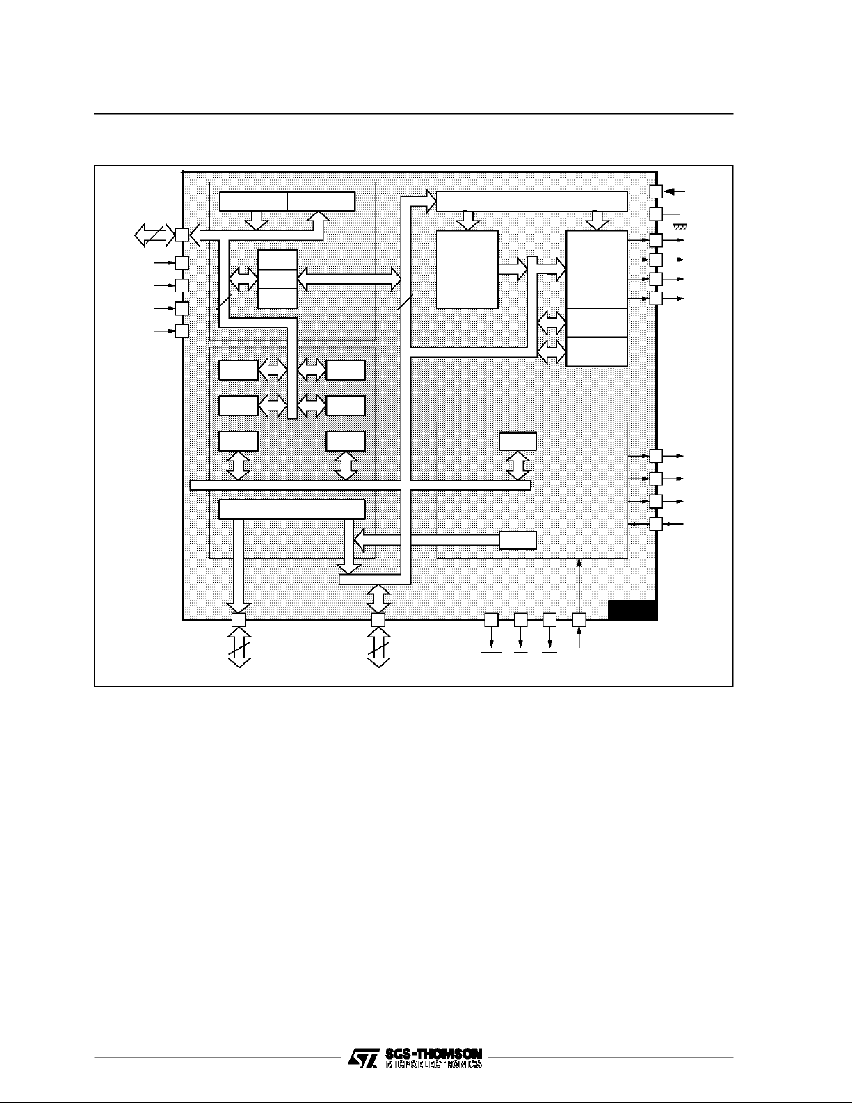
BLOCK DIAGRAM
EF9345
AD(0:7)
AS
STA CMD
8
14
15DS
16R/W
16CS
MPU ACCESS
8
R3R4
R3R6
R3ROR
TRANSCODER
ADDRESS UNIT
R1
R2
R3
R3R5
R3R7
R3DOR
8
DATA BUS
ROW BUFFER 120 x 8
ROM
R3TSG
R3RFSH
ATTRIBUTE
LOGIC
MAT
PAT
TIMING
GENERATOR
+5V
R
9
G
8
B
7
I
10
11
HP
HVS/HS
5
5
PC/VS
6
6
13
SYNC.IN
AM(8:13)
R3
3
2
4
6
ADM(0:7)
8
WE
OE
ASM
CLK
EF9345
12
9345-02.EPS
3/38

EF9345
ABSOLUTEMAXIMUM RATINGS
Symbol Parameter Value Unit
* Supply Voltage -0.3, 7.0 V
V
CC
* Input Voltage -0.3, 7.0 V
V
in
T
A
T
stg
P
Dm
* With respect to Vss.
Stresses above those hereby listed may cause permanent damage tothe device. The ratings are stress ones only and functional operation of
the device atthese or any conditionsbeyond thoseindicatedinthe operational sectionsof this specificationis notimplied. Exposure tomaximum
rating conditionsfor extendedperiods may affect reliability. StandardMOS circuits handlingprocedure should be used toavoid possibledamage
to the device.
Operating Temperature 0, +70
Storage Temperature -55, +150
Maximum Power Dissipation 0.75 W
ELECTRICAL CHARACTERISTICS
=5.0V ±5%, VSS=0V,TA= 0 to +70°C,unless otherwisespecified.
V
CC
Symbol Parameter Min. Typ. Max. Unit
V
CC
V
IL
V
IH
I
IN
V
OH
V
OL
P
D
C
IN
I
TSI
Supply Voltage 4.75 5 5.25 V
Input Low Voltage -0.3 0.8 V
Input HighVoltage : CLK
Other Inputs
2.2
2
V
CC
V
CC
Input Leakage Current 10 µ
Output HighVoltage (I
Output Low Voltage : I
= -500µA)
load
= 4mA ; AD(0:7), ADM(0:7), AM(8:13)
load
= 1mA ; Other Outputs
I
load
2.4 V
0.4
0.4
Power Dissipation 250 mW
Input Capacitance 15 pF
Three State (Off State) Input Current 10 µ
o
C
o
C
V
A
V
A
9345-02.TBL
9345-03.TBL
4/38

EF9345
MEMORYINTERFACE
=5.0V ±5%, TA=0 to + 70°C
V
CC
Clock : f
ReferenceLevels: V
Symbol Ident. N° Parameter Min. Typ. Max. Unit
t
ELEL
t
EHEL
t
ELDV
t
t
AVEL
t
ELAX
t
CLAZ
t
GHDX
t
t
GLDV
t
QVWL
t
WHQX
t
WLWH
= 12MHz ; DutyCycle 40 to 60% ; tr,tf< 5ns
in
= 0.8Vand VIH=2V,VOL= 0.4V and VOH=2.4V
IL
1 Memory Cycle Time 500 ns
t
D
2 Output Delay Time from CLK Rising Edge (ASM, OE, WE) 60 ns
3 ASM High Pule Width 120 ns
4 Memory Access Time from ASM Low 290 ns
DA
5 Output Delay Time from CLK Rising Edge (ADM(0:7), AM(8:13)) 80 ns
6 Address Setup Time to ASM 30 ns
7 Address Hold Time from ASM 55 ns
8 Address Off Time 80 ns
9 Memory Hold Time 10 ns
OZ
10 Data Off Time from OE 60 ns
11 Memory OE Access Time 150 ns
12 Data Setup Time (Write Cycle) 30 ns
13 Data Hold Time (WriteCycle) 30 ns
14 WE Pulse Width 110 ns
9345-04.TBL
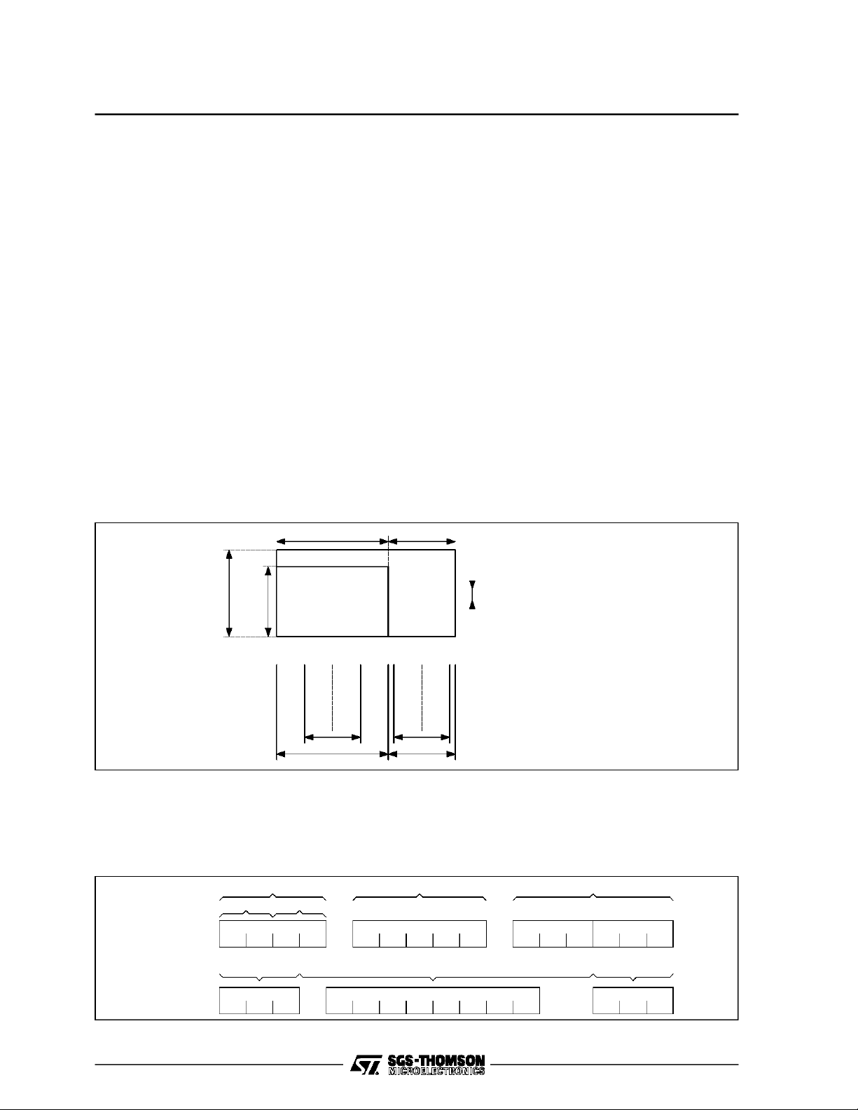
Figure 1 : TestLoad Table 1
V
DD
Symbol
C 100pF 50pF
R
Test
Point
R
L
C
L
R
MMD7000
or equivalent
R
9345-03.EPS
Figure 2 : Memory Interface Timing Diagram
1
2
D
2
11
3
56 7
IN
9
10
CLK
ASM
ADM (0:7)
AM (8:14)
OE
WE
T
2
56 7
READ ADDRESS WRITE ADDRESS
4
8
2
AM(8:13)
ADM(0:7)
AD(0:7)
L
1kΩ 3.3kΩ
4.7kΩ 4.7kΩ
5
D
OUT
22
12 13
14
Other
Outputs
9345-05.TBL
9345-04.EPS
5/38

EF9345
MICROPROCESSORINTERFACE
EF9345 is motel compatible. It automaticallyselects the processortype by using AS input latch to
state of the DS input.
No external logic is needed to adapt bus control
signals frommost of the common multiplexed bus
microprocessors.
MICROPROCESSORINTERFACE TIMING AD(0:7), AS, DS, R/W, CS
V
= 5.0V ±5%,TA= 0 to + 70°C, CL=100pF on AD(0:7)
CC
ReferenceLevels : V
Symbol Ident. N° Parameter Min. Typ. Max. Unit
t
CYC
t
ASD
t
ASED
t
PWEH
t
PWASH
t
RWS
t
RWH
t
ASL
t
AHL
t
DSW
t
DHW
t
DDR
t
DHR
t
ACC
1 Memory Cycle Time 400 ns
2
3
4 Write Pulse Width 200 ns
5 AS Pulse Width 100 ns
6 R/W to DS Setup Time (Timing 1) 100 ns
7 R/W to DS Hold Time (Timing 1) 10 ns
8 Address and CS Setup Time 20 ns
9 Address and CS Hold Time 20 ns
10 Data Setup Time (Write Cycle) 100 ns
11 Data Hold Time (Write Cycle) 10 ns
12 Data Access Time from DS (Read Cycle) 150 ns
13 DS Inactive to High Impedance State Time (Read Cycle) 10 80 ns
14 Address to Data Valid Access Time 300 ns
=0.8V and VIH=2V on All Inputs ; VOL= 0.4V andVOHonall Outputs.
IL
DS Low to AS High (Timing 1)
DS High or R/W High to AS High (Timing 2)
AS Low to High (Timing 1)
AS Low to DS Low or R/W Low (Timing 2)
EF9345 6801 INTEL Family
Timing 1 Timing 2
AS AS ALE
DS
DS, E, φ 2
RD
R/W R/W WR
30 ns
30 ns
9345-06.TBL
Figure 3 : MicroprocessorInterfaceTiming Diagram1 (6801 Type)
1
3
2
5
6
8
ADDRESS
8
ADDRESS
9
9
12
14
6/38
DS
ASM
R/W
CS
WRITECYCLE
AD (0:7)
READ CYCLE
AD (0:7)
10
INPUT DATA
OUTPUT
DATA
2
7
11
13
9345-05.EPS

Figure 4 : MicroprocessorInterfaceTiming Diagram2 (INTEL Type) - ReadCycle
1
EF9345
ALE
(Pin AS)
23
5
RD
(Pin DS)
WR
(Pin R/W)
2
12
CS
AD(0:7)
8
9
ADDRESS
14
13
D
OUT
Figure 5 : MicroprocessorInterfaceTiming Diagram2 (INTEL Type) - Write Cycle
1
ALE
(Pin AS)
RD
(Pin DS)
2
2
5
3
4
9345-06.EPS
WR
(Pin R/W)
CS
AD(0:7)
89
ADDRESS
10
11
D
IN
9345-07.EPS
7/38
EF9345
VIDEO INTERFACE R, G, B, I, HP, HVS/HS, PC/VS
V
= 5.0V ±5%,TA= 0 to + 70°C, CLK Duty Cycle = 50%, CL=50pF
CC
ReferenceLevels : V
Symbol Parameter Min. Typ. Max. Unit
t
t
HO
t
t
PWCH
t
PWCL
Setup Time R, G, B, I to HP 10 ns
SU
Hold Time R, G, B, I fromHP 50 ns
Output Delay from CLK Edge 60 ns
D
CLK High Pulse Width 30 ns
CLK Low Pulse Width 30 ns
Figure6
CLK
=0.8V and VIH=2.2V on CLK Inputs.VOL=0.4V and VOH= 2.4V on all Outputs.
IL
9345-07.TBL
R, G, B, I,
40 char/row
HP
R, G, B, I,
80 char/row
HVS/HS
PC/VS
INPUT CLK
CLK
t
D
t
HO
t
SU
t
D
t
D
t
PWCH
t
PWCL
t
D
t
D
t
D
8/38
9345-08.EPS
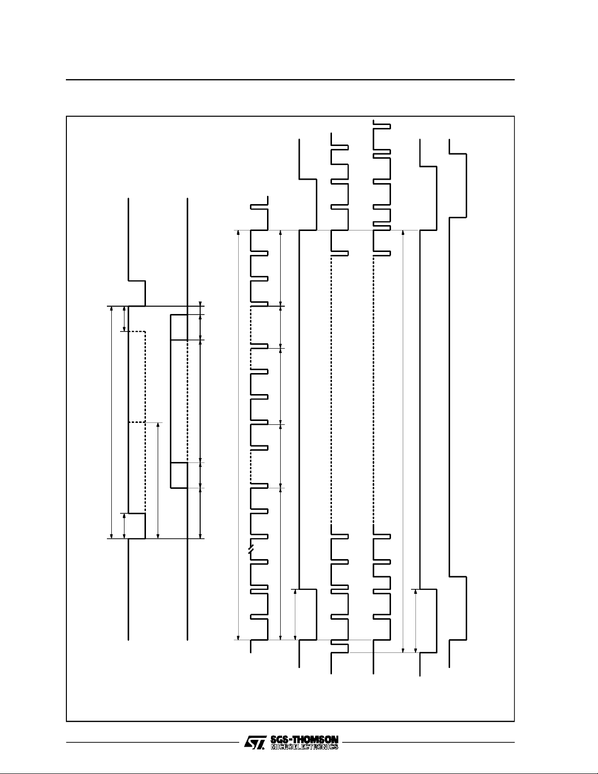
Figure 7 : Vertical and Horizontal SynchronizationOutputs (CLK = 12MHz)
Blanking 3 Lines
2.04µs
4.5µs4.5µs
Margin
18 Lines
EF9345
Bulk
40µs6µs2µs
40µs6µs6µs
=0)
=1)
0
312 lines (TGS
0
362 lines (TGS
64µs
6µs40 char/row
Margin Margin H BlankingH Blanking
32µs
Odd frame 1/2 pulse Even frame 1/2 pulse
10µs
9.96µs
=0)
0
312.5 lines (TGS
=1)
0
362.5 lines (TGS
80 char/row
Blanking 25 Lines Margin 16 Lines Page 250 Lines
2 lines
2.5 lines
=0)
4
HVS
OHVOL
V
=0
= 1 25 Lines 10 Lines 210 Lines 14 Lines 3Lines
0
R, G, B, I
=1)
0
4
TGS
TGS
=0)
4
=1)
4
HORIZONTAL SYNCHRO
VERTICAL SYNCHRO
NON INTERLACED
HVS (TGS
VS (TGS
INTERLACED
Even Frame
HVS (TGS
Odd Frame
Even Frame
VS (TGS
Odd Frame
9345-09.EPS
9/38

EF9345
FUNCTIONAL DESCRIPTION
The EF9345is a low cost, semigraphic,CRT controller.
It is optimizedfor use witha lowcost, monochrome
or color TV type CRT (64ms per line, 50 or 60Hz
refresh frequency).
The EF9345 displays up to 25 rows of 40 characters or 25 rows of 80 characters.
The on-chip character generator provides a 128
standard, 5 x 7, character set and standard semigraphic sets.
More usedefinable(8 x 10) alphanumericor semigraphicsets may bemappedin the16K x8 private
memory addressingspace.
These user definable sets are available only in 40
charactersper row format.
MicroprocessorInterface
The EF9345 provides an 8-bit, adress/data multiplexed microprocessorinterface.
It is directly compatible with popular (6801, 8048,
8051, 8035,...) microprocessors.
40 Charactersper Row : Character Code
Formatsand Attributes
Once the 40 characters per row format has been
selected, one character code format out of three
must be chosen :
- 24-bit fixed format :
All the attributesare providedin parallel.
- 8/24-bit compressedformat :
All the attributesare latched.
- 16-bit fixed format :
Some parallel attributes,other are latched.
Characterattributesprovided :
- Backgroundand foregroundcolor (3 bits each),
- Doubleheight, double width,
- Blinking,
- Reverse,
- Underlining,
- Conceal,
- Insert,
- Accentuationof lower casecharacters,
- 3 x 100 user definable character generator in
memory,
- 8 x 100semi-graphicquadrichromecharacters.
Registers
The microprocessordirectly accesses8 registers:
- R0 : Command/status register.
- R1, R2, R3 : Data registers.
- R4, R5, R6, R7 : Each of these register pairs
pointsinto the private memory.
Through these registers, the microprocessorindirectly accesses the private memory and 5 more
registers :
- ROR, DOR : Base address of displayed page
memoryand usedexternalcharactergenerators.
- PAT, MAT, TGS : Usedto select the page attributes and format, and to program thetiming generatoroption.
Private Memory
The usermay partitionthe 16Kx 8 private memory
addressingspace between :
- Page ofcharacter codes(2 K x 8 or 3 K x 8),
- Externalcharacter generators,
- Generalpurposeuser area.
Many types of memory componentsare suitable :
- ROM, DRAMor SRAM,
- 2 K x 8, 8 K x 8, 16 K x 4 organizations,
- Modest 500ns cycletime and 250nsaccess time
is required.
80 Charactersper Row Format : Character
Code Format and Attributes
Two character code formats are provided :
- Long (12 bits)with 4 parallel attributes:
• Blinking,
• Underlining,
• Reverse,
• Color select.
- Short (8 bits) : no attributes.
Timing Generator
The whole timing is derived from a 12MHz main
clock input.
The RGB outputs are shifted at 8MHz for the 40
character/row format and at 12MHz for the 80
character/row.
Besides,the user mayselect :
- 50Hz or 60Hzvertical sync. frequency,
- Interlacedor not,
- Separated or composite vertical and horizontal
sync.ouputs.
Furthermore,a compositesync.inputallows,when
it is required :
- An on-chip vertical resynchronization,
- An on-chip crude horizontalresynchronization,
- An off-chip high performance horizontal resynchronization by use of a simple external VCXO
controlledby theon-chip phase comparator.
10/38

MEMORYORGANIZATION
Logical And PhysicalAddressing
The physical16-Kbyteaddressingspaceis logicaly
partitioned by EF9345 into 40-byte buffers (Figure 8). Moreprecisely,a logicaladdressisgiven by
an X, Y,Z triplet where :
- X = (0 to 39) points to a byte inside a buffer,
- Y = (0, 1 ; 8 to 31) points to a buffer inside a
1 Kbyte blocks,
- Z = (0 to 15) points to a block.
Obviously, 1 K = 2
10
= 1024 cannot be exactly
divided by 40. Consequently, any block holds 25
full buffersand a24-byte remainder.Provided that
the physicalmemory is a multiple of 2 Kbytes, the
remainders are paired in sucha way as to make
available:
- A full buffer (Y = 1) in each evenblock,
- A partial buffer (Y = 1 ; X = 32 to 39)in each odd
block.
Figure 8 : Memory Row Buffer
EF9345
Pointers
EachX, Y and Z componentof alogical address is
binaryencodedand packed in two 8-bitsregisters.
Sucha registerpair is a pointer (Figure9). EF9345
containstwo pointers :
- R4, R5 : auxiliary pointer,
- R6, R7 : main pointer.
R5 and R7 have the same format. Each one holds
an X componentand the two LSB’sof a Z component. This packing induces a partitioning of Z in 4
districts of 4 blockseach.
R5, R7 points to a block number in a district. R4
and R6 have a slightlydifferent format : Each one
holds a Y component and the LSB of the district
number. But R6 holds bothdistrictMSB
Figure 11 gives the logical to physical address
transcodingscheme performed onchip.
Figure9 : PointerAuto Incrementation
X
839
32 32
DISTRICT
0
1
8
31
00
1
8
Y
31
0
1
8
31
0
1
8
31
0
9
DISTRICT
DISTRICT
120-BYTE ROW BUFFER 80-BYTE ROW BUFFER
- Row buffers lay indide a district
Notes :
- At two or threesuccessiveblock addresses (modulo 4)
- First block address is even
BLOCK0
(1Kbyte)
BLOCK1
BLOCK2
BLOCK3
839
X
Y
39 1
9345-10.EPS
Y = (0, 1 ; 8 to 31)
d1d’1d043210R6
X=0to39
b0b1543210R7
Y’ = (0, 1 ; 8 to 31)
__
b’0b’1543210R5
X incrementation
d’043210R4
X’ = 0 to 39
0
2=0
4=0
6=0
0
XYB
Modulo40
89
31
2
Y incrementation
1
3=1
5=1
7=1
Modulo24
MAIN
POINTER
AUXILIARY
POINTER
Z = (0 to 15)
3210
DB
1
10
0
3
Z incrementation/
decrementation
Modulo4 on the
blocknumber only
2
9345-11.EPS
11/38
EF9345
Data Structure in Memory
A page is a data structure displayable on the
screen up to 25 rows of characters. According to
the charactercode format, eachrow on the screen
is associatedwith 2 (or 3)40-bytebuffers. This set
of 2 (or 3) buffers constitutes a row buffer (Figure 8). Thebuffers belongingto arow buffer must
meet the followingrequirements :
- They have the same Y address,
- They have the same district number,
- They lie at 2 (or 3) successive (modulo 4) block
addressesin their common district.
Consequently, a row buffer is defined by its first
buffer address andits format.
A pageis a set of successiverow buffers :
- With thesame format,
- With thesame districtnumber,
- With the same block address of first buffer. This
blockaddress must be even,
- Lyingat successive(modulo 24) Y addresses.
Figure 10 : MemoryCycle Allocation
40µs24µs
Consequently, a page should not cross a district
boundary.General purpose memory area may be
used but should respect the buffer of row buffer
structure. See Figure 9 for pointer incrementation
implied by these data structures.
MemoryTime Sharing (See Figure10)
Thememoryinterfaceprovidesa 500ns cycletime.
Thatis to say a 2 Mbyte/smemory bandwith. This
bandwithis shared between :
- Reading a row buffer from memory to load the
internalrowbuffer(upto120bytesonceeachrow),
- Readinguser definedcharactersslicesfrom memory (1 byte each µs),
- Indirectmicroprocessor read or write operation,
- Refreshcycles to allowDRAM use, withno overhead.
A fixed allocation schemeimplements the sharing.
During these lines, no microprocessor access is
provided for 104µs ; this hold too when no user
definedcharacter slices are addressed.
312/362
250/210
SCAN
ACTIVE
LINES
SCAN
LINES
INACTIVE LINE
LAST ROW LINE
FIRST ROW LINE
OTHER ROW LINE
Notes : 1. Dummy cycles are read cycles at dummyaddresses.
2. RFSH cycles are read cycles performed by an 8-bit auto-incrementing counter. Low order address byte ADM(0:7) cycles
through its 256 statesin less than 1ms.
3.
The microprocessor may indirectly access the memory once every µs, except during the first and the last line of a row, when
the internalbuffer must be reloaded.
ACTIVE
DISPLAY
TIME
DUM
µP
UDS
LD
UDS
LD
UDS
µP
1µs
40µs24µs
RFSH
LD
RFSH
RFSH
µP
LD
µP
µP
1µs
ONE ROW = 10 SCAN LINES
MEMORY CYCLE
DUM : dummy cycle
µP : indirect access to memory
RFSH : refresh cycle
UDS :slice read cycle
LD : read cycle to load the internal row buffer
Figure 11 : Logicalto PhysicalAddress TranscodingPerformed On-chip
Z (0 to 15) Y (0, 1 ; 8 to 31) X (0 to 39)
DB
LOGICAL
ADDRESS
3210 43210 43210
TRANSCODING
5
9345-12.EPS
12/38
PHYSICAL
ADDRESS
131211 109876543 210
9345-13.EPS
 Loading...