


®
MAIN PRODUCTS CHARACTE RISTICS
DTVseries
(CRT HORIZO N TAL DEF LEC T ION)
HIGH VOLTAGE DAMPER DIODE
I
F(AV)
V
RRM
V
F
5 A to 10 A
1500 V
1.3 V to 1.5 V
FEATURES AND BENEFITS
HIGH BREAKDOWN VOLTAGE CA PABILITY
VERY FAST RECOVERY DIODE
SPECIFIED TURN ON SWITCHING
CHARACTERISTICS
LOW STATIC AND PE AK FORWARD VOLTAGE
DROP FOR LOW DISSIPATION
SUITED TO 32-110kHz MONITORS AND
16kHz TV DEFLECTION
INSULATED VERSION (ISOWA TT220AC):
Insulating voltage = 2000V DC
Capacitance = 12pF
PLANAR TECHNOLOGY ALLOWING HIGH
QUALITY AND BEST ELECTRICAL
CHARACTERISTICS
A
TO-220AC
DTVxxxD
A
K
ISOWATT220AC
DTVxxxF
K
DESCRIPTION
High voltage diode with high current capability
dedicated to horizontal deflection. DTV16 is
optimized to TV meanwhile DTV32 to DTV110 are
covering the full range of monitors from the low
end to the professional hi-definition SXGA CAD
display units.
These devices are packaged either in TO220-AC
or in ISOWATT220AC.
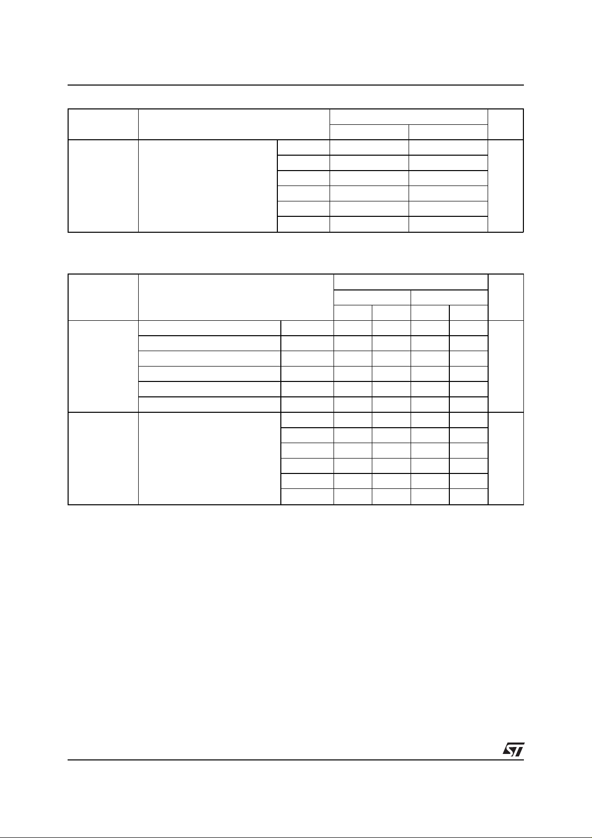
ABSOLUTE RATINGS
Symbol Parameter Value Unit
V
RRM
I
F(RMS)
I
FSM
Repetitive peak reverse voltage 1500 V
RMS forward current 15 A
Surge non repetitive forward current
tp = 10ms half sine wave
DTV16 50 A
DTV32 75
DTV56 80
DTV64 80
DTV82 80
DTV110 80
T
stg
T
j
August 1999 - Ed: 2B
Storage temperature range -65 to 150 ° C
Maximum operating junction temperature 150 ° C
1/10
DTVseries
THERMAL RESISTANCES
Symbol Parameter
R
th(j-c)
Junction to case thermal
resistanc e
STATIC ELECTRICAL CHARACTE RISTICS
Symbol Test Conditions
V
F *
I
R **
pulse test : * tp = 380 µs, δ < 2%
** tp = 5 ms, δ < 2%
IF = 5 A DTV16 1.6 1.0 1.5 V
= 6 A DTV32 1.5 1.1 1.35
I
F
= 6 A DTV56 1.8 1.1 1.5
I
F
= 6 A DTV64 1.7 1.1 1.4
I
F
= 6 A DTV82 1.8 1.0 1.3
I
F
= 10 A DTV110 2.3 1.15 1.5
I
F
VR = V
RRM
Value
TO-220AC ISOWATT220AC
Unit
DTV16 3 5.5 °C/W
DTV32 2.5 4.75
DTV56 2 4
DTV64 1 .8 4
DTV82 1.6 3.7
DTV110 1.3 3.5
Value
UnitTj = 25°C Tj = 125°C
Typ Max Typ Max
DTV16 60 100 500
A
µ
DTV32 100 100 1000
DTV56 100 100 1000
DTV64 100 100 1000
DTV82 100 100 1000
DTV110 100 100 1000
2/10

DTVseries
RECOVERY CHARA CTERISTICS
Symbol Test Conditions Typ Max Unit
t
rr
t
rr
IF = 100m A
I
= 100mA
R
I
= 10mA
RR
IF = 1 A
dI
/dt =-50A/µs
F
V
=30V
R
TURN-ON SWITCHING CHARACT ERISTICS
Tj = 25°C DTV16 1500 ns
DTV32 850
DTV56 750
DTV64 750
DTV82 675
DTV110 625
Tj = 25°C DTV16 200 300 ns
DTV32 130 175
DTV56 110 135
DTV64 110 135
DTV82 105 125
DTV110 95 115
Symbol Test Conditions Typ Max Unit
t
fr
IF = 6 A
dI
/dt = 80 A/µs
F
V
=3V
FR
Tj = 100°C DTV16 350 ns
DTV32 570
DTV56 350
DTV64 350
DTV82 270
DTV110 250
V
FP
IF = 6A
dI
/dt = 80 A/µs
F
Tj = 100°C DTV16 25 34 V
DTV32 21 28
DTV56 19 26
DTV64 18 22
DTV82 14 18
DTV110 11 14
To evaluate the maximum conduction losses use the following equation :
DTV16 P= 1.14 x I
DTV32 P= 1.069 x I
DTV56 P= 1.15 x I
DTV64 P= 1.06 x I
DTV82 P= 1.01 x I
DTV110 P= 1.12 x I
F(AV)
F(AV)
F(AV)
F(AV)
F(AV)
F(AV)
+ 0.072 x I
+ 0.047 x I
+ 0.059 x I
+ 0.053 x I
+ 0.048 x I
+ 0.038 x I
F2(RMS)
F2(RMS)
F2(RMS)
F2(RMS)
F2(RMS)
F2(RMS)
3/10

DTVseries
Fig. 1-1:
Power dissipation versus peak forward
current (triangular waveform, δ=0.45).
PF(av)(W)
3.5
3.0
2.5
2.0
1.5
DTV16
DTV110
1.0
0.5
0.0
0246810
Fig. 1-3:
Power dissipation versus peak forward
Ip(A)
current (triangular waveform, δ=0.45).
PF(av)(W)
2.0
1.5
Fig. 1- 2:
Power dissipation versus peak forward
current (triangular waveform, δ=0.45).
PF(av)(W)
2.0
1.5
DTV32
1.0
0.5
0.0
0123456
DTV56
Ip(A)
DTV82
1.0
DTV64
0.5
Ip(A)
0.0
0123456
Fig. 2-1:
Average current versus case temperature
(δ=0.5) (TO-220AC).
IF(av)(A)
12
10
8
DTV64
DTV56
DTV32
6
4
T
DTV16
2
=tp/T
δ
0
0 25 50 75 100 125 150
tp
Tcase(°C)
DTV110
DTV82
Fig. 2-2:
Average current versus case temperature
(δ=0.5) (ISOWATT220AC).
IF(av)(A)
12
10
8
DTV32
DTV56
DTV64
6
4
T
DTV16
2
Tcase(°C)
=tp/T
δ
0
0 25 50 75 100 125 150
tp
DTV110
DTV82
4/10

DTVseries
Fig. 3-1:
Forward voltage drop versus forward
current (DTV16D/F).
IFM(A)
20.0
10.0
1.0
Typical
Tj=125°C
Maximum
Tj=125°C
Maximum
Tj=25°C
VFM(V)
0.1
0.0 0.2 0.4 0.6 0.8 1.0 1.2 1.4 1.6 1.8 2.0 2.2
Fig. 3-3:
Forward voltage drop versus forward
current (DTV56D/F).
IFM(A)
20.0
10.0
1.0
Typical
Tj=125°C
Maximum
Tj=125°C
Maximum
Tj=25°C
Fig. 3-2:
Forward voltage drop versus forward
current (DTV32D/F).
IFM(A)
20.0
10.0
1.0
0.1
0.0 0.2 0.4 0.6 0.8 1.0 1.2 1.4 1.6 1.8 2.0
Fig. 3-4:
Forward voltage drop versus forward
Maximum
Tj=125°C
Typical
Tj=125°C
Maximum
Tj=25°C
VFM(V)
current (DTV64D/F).
IFM(A)
20.0
10.0
1.0
Maximum
Tj=125°C
Typical
Tj=125°C
Maximum
Tj=25°C
0.1
0.00 0.25 0.50 0.75 1.00 1.25 1.50 1.75 2.00 2.25 2.50
Fig. 3-5:
Forward voltage drop versus forward
VFM(V)
current (DTV82D/F).
IFM(A)
20.0
10.0
1.0
0.1
0.00 0.25 0.50 0.75 1.00 1.25 1.50 1.75 2.00 2.25 2.50
Typical
Tj=125°C
Maximum
Tj=125°C
VFM(V)
Maximum
Tj=25°C
0.1
0.0 0.2 0.4 0.6 0.8 1.0 1.2 1.4 1.6 1.8 2.0 2.2
Fig. 3-6:
Forward voltage drop versus forward
current (DTV110D/F).
IFM(A)
VFM(A)
20.0
10.0
1.0
0.1
0 0.5 1 1.5 2 2.5 3
Typical
Tj=125°C
Maximum
Tj=125°C
VFM(V)
Maximum
Tj=25°C
5/10

DTVseries
Fig. 4-1:
Non repetitive surge peak forward current
versus overload duration (TO-220AC)
(DTV16D / DTV32D / DTV56D).
IM(A)
60
55
50
45
DTV32D & DTV56D
Tc=100°C
40
35
30
DTV16D
25
20
15
I
M
10
5
0
1E-3 1E-2 1E-1 1E+0
Fig. 4-3:
t
δ
=0.5
t(s)
Non repetitive surge peak forward current
versus overload duration (TO-220AC)
(DTV64D / DTV82D / DTV110D).
IM(A)
100
90
80
70
DTV110D
DTV82D
60
50
DTV64D
40
30
I
M
20
10
0
1E-3 1E-2 1E-1 1E+0
t
δ
=0.5
t(s)
Tc=100°C
Fig. 4-2:
Non repetitive surge peak forward current
versus overload duration (ISOWATT220AC)
(DTV16F / DTV32F / DTV56F).
IM(A)
45
40
35
DTV32F & DTV56F
Tc=100°C
30
25
DTV16F
20
15
I
M
10
5
0
1E-3 1E-2 1E-1 1E+0
Fig. 4-4:
t
δ
=0.5
t(s)
Non repetitive surge peak forward current
versus overload duration (ISOWATT220AC)
(DTV64F / DTV82F / DTV110F).
IM(A)
60
55
50
45
DTV110F
DTV82F
40
35
30
25
DTV64F
20
15
I
M
10
5
0
1E-3 1E-2 1E-1 1E+0
t
δ
=0.5
t(s)
Tc=100°C
Fig. 5.1:
Reverse recovery charges versus dIF/dt
(DTV16D/F).
Qrr(µC)
2.4
IF=Ip
2.2
90% confidence
2.0
Tj=125°C
1.8
1.6
1.4
1.2
1.0
0.8
0.6
0.4
0.2
0.0
0.1 0.2 0.5 1.0 2.0 5.0
6/10
dIF/dt(A/µs)
Fig. 5.2:
Reverse recovery charges versus dIF/dt.
Qrr(nc)
1200
1000
800
600
IF=Ip
90% confidence
Tj=125°C
DTV64
DTV32
DTV82
400
200
dIF/dt(A/µs)
0
0.1 0.2 0.5 1 2 5

DTVseries
Fig. 5.3:
Reverse recovery charges versus dIF/dt.
Qrr(nc)
1200
1000
IF=Ip
90% confidence
Tj=125°C
DTV56
800
600
DTV110
400
200
dIF/dt(A/µs)
0
0.1 0.2 0.5 1 2 5
Fig. 6.2:
2.2
2.0
1.8
1.6
1.4
1.2
1.0
0.8
Reverse rec overy curr ent ver sus dIF/dt.
IRM(A)
IF=Ip
90% confidence
Tj=125°C
DTV64
DTV110
0.6
0.4
0.2
0.0
0.1 0.2 0.5 1 2 5
dIF/dt(A/µs)
Fig. 6.1:
3.0
2.7
2.4
Reverse recovery current versus dIF/dt.
IRM(A)
IF=Ip
90% confidence
Tj=125°C
2.1
1.8
DTV16
1.5
1.2
DTV32
0.9
0.6
0.3
0.0
0.1 0.2 0.5 1 2 5
Fig. 6.3:
2.2
2.0
1.8
Reverse rec overy curr ent ver sus dIF/dt.
IRM(A)
IF=Ip
90% confidence
Tj=125°C
dIF/dt(A/µs)
1.6
1.4
1.2
DTV56
1.0
0.8
0.6
DTV82
0.4
0.2
0.0
0.1 0.2 0.5 1 2 5
dIF/dt(A/µs)
Fig. 7-1:
Transient peak forward voltage versus
dIF/dt.
VFP(V)
45
IF=Ip
40
90% confidence
Tj=125°C
35
30
DTV32
25
20
15
10
5
0
0 20 40 60 80 100 120 140
DTV16DTV16DTV16
DTV56
dIF/dt(A/µs)
Fig. 7.2:
Transient peak forward voltage versus
dIF/dt.
VFP(V)
30
IF=Ip
90% confidence
25
Tj=125°C
20
DTV82
15
10
5
0
0 20 40 60 80 100 120 140
DTV64
DTV110
dIF/dt(A/µs)
7/10

DTVseries
Fig. 8.1:
Forward recovery time versus dIF/dt.
tfr(ns)
800
750
IF=Ip
90% confidence
Tj=125°C
700
650
DTV32
600
550
500
450
400
Fig. 9:
DTV16DTV16DTV16
dIF/dt(A/µs)
0 20 40 60 80 100 120 140
Dynamic parameters versus junction
DTV64
temperature.
VFP,IRM,Qrr[Tj]/VFP,IRM,Qrr[Tj=125°C]
1.2
1.0
Fig. 8-2:
700
650
Forward recov ery time versu s dIF/d t.
tfr(ns)
IF=Ip
90% confidence
Tj=125°C
600
550
500
450
400
350
300
Fig. 10:
DTV110
dIF/dt(A/µs)
0 20 40 60 80 100 120 140
Junction capacitance versus reverse
DTV56
DTV82
voltage applied (typical values).
C(pF)
200
100
DTV110
DTV82
Tj=25°C
F=1MHz
0.8
0.6
VFP
0.4
IRM
0.2
0.0
Fig. 11-1:
Qrr
Tj(°C)
0 20 40 60 80 100 120 140
Relative variation of thermal impedance
junction to case versus pulse duration
(ISOWATT220AC).
K=[Zth(j-c)/Rth(j-c)]
1.0
δ = 0.5
0.5
δ = 0.2
δ = 0.1
0.2
Single pulse
tp(s)
0.1
1E-2 1E-1 1E+0 1E+1
δ
=tp/T
T
tp
DTV16DTV16DTV16
10
1
1
Fig. 12-2:
Relative variation of thermal impedance
DTV32
DTV56
DTV64
VR(V)
10 100 200
junction to case versus pulse duration
(TO-220AC).
K=[Zth(j-c)/Rth(j-c)]
1.0
δ = 0.5
0.5
δ = 0.2
δ = 0.1
0.2
Single pulse
tp(s)
0.1
1E-3 1E-2 1E-1 1E+0
δ
=tp/T
T
tp
8/10

PACKAGE DAT A
TO-220AC (plastic) (JE DEC outline)
H2
L5
Ø I
L6
L2
L9
F1
L4
F
G
DTVseries
DIMENSIONS
REF.
A
C
A 4. 40 4.60 0.173 0.181
C 1.23 1.32 0.048 0.051
L7
D 2.40 2.72 0.094 0.107
E 0. 49 0.70 0.019 0.027
F 0.61 0.88 0.024 0.034
F1 1.14 1.70 0.044 0.066
D
G 4.95 5.15 0.194 0.202
H2 10.00 10.40 0.393 0.409
L2 16.40 typ. 0.645 typ.
M
E
L4 13.00 14.00 0.511 0.551
L5 2.65 2.95 0.104 0.116
L6 15.25 15.75 0.600 0.620
L7 6.20 6.60 0.244 0.259
L9 3.50 3.93 0.137 0.154
M 2.6 typ. 0.102 typ.
Diam. I 3.75 3.85 0.147 0.151
Millimeters Inches
Min. Max. Min. Max.
Cooling method : c.
Torque value : 0.55 m.N typ (0.70 m.N max).
9/10

DTVseries
PACKAGE DATA
ISOWATT220AC (plastic)
H
L6
L2
L3
F1
F
G
A
B
Diam
D E
Cooling method : C.
Torque value : 0.55 m.N typ (0.70 m.N max).
DIMENSIONS
REF.
Millimeters Inches
Min. Typ. Max. Min. Typ. Max.
A 4.40 4.60 0.173 0.181
B 2.50 2.70 0.098 0.106
D 2.40 2.75 0.094 0.108
L7
E 0.40 0.70 0.016 0.028
F 0.75 1.00 0.030 0.039
F1 1.15 1.70 0.045 0.067
G 4.95 5.20 0.195 0.205
H 10.00 10.40 0.394 0.409
L2 16.00 0.630
L3 28.60 30.60 1.125 1.205
L6 15.90 16.40 0.626 0.646
L7 9.00 9.30 0.354 0.366
Diam 3.00 3.20 0.118 0.126
Electrical isolation : 2000V DC
Capacitance : 12 pF
Ordering code Marking Package Weight Base qty Delivery mode
DTV16D
DTV32D
DTV56D
DTV64D
DTV82D
DTV110D
DTV16F
DTV32F
DTV56F
DTV64F
DTV82F
DTV110F
DTV16D
DTV32D
DTV56D
DTV64D
DTV82D
DTV110D
DTV16F
DTV32F
DTV56F
DTV64F
DTV82F
DTV110F
TO-220AC 1.86g 50 Tube
ISOWATT220AC 2g 50 Tube
Epoxy meets UL94, V0
Information furnished is believed to be accurate and reliable. However, STMicroelectronics assumes no responsibility for the consequences of
use of such information nor for any infringement of patents or other rights of third parties which may result from its use. No license is granted by
implication or otherwi se un der any pat ent or patent rights of STMic roelec tronics. S pecifications ment ioned in t his publ ication are subject to
change without notice. This publication supersedes and replaces all information previously supplied.
STMicroelectronics products ar e not authorized for use as critical components in l i fe s upport devices or systems without express written approval of STMicroelectronics.
The ST logo is a registered trademark of STMicroe lectronics
© 1999 STMicroelectronics - Printed in Italy - All rights reser ved.
STMicroelectronics GROUP OF COMPANIES
Australia - Brazil - China - Finland - France - Germany - Hong Kong - India - Italy - Japan - Malaysia
Malta - Morocco - Singapore - Spain - Sweden - Switzerland - United Kingdom - U.S.A.
http://www.st.com
10/10
 Loading...