

DSM (Digital Signal Processor System Memory)
For Analog Devices ADSP-2191 DSPs (3.3V Supply)
FEATURES SUMMARY
■ Glueless Connection to DSP
– Easily add memory, logic, and I/O to the Exter-
nal Port of ADSP-2191 DSP
■ Dual Flash Memories
– Two independent Flash memory arrays for stor-
ing DSP code and data. DSP may access the
two arrays concurrently (read from one while
erasing or writing the other)
– 256K x 8 Main Flash memory divided into 8 sec-
tors (32KByte each)
– Ample storage for booting DSP code/data
upon reset and subsequent code swaps
– Large capacity for data recording
– 32K x 8 Secondary Flash memory divided into 4
sectors (8 KByte each). Multiple uses:
– Small sector size ideal for small data sets,
and calibration or configuration constants
– Store custom start-up code in one or more
sectors and configure DSP to run from external memory upon reset (no boot)
– Concatenate Secondary Flash with Main
Flash for total of 288 KBytes
– Each Flash sector can be write protected.
– Built-in programmable address decoding logic
allows mapping individual Flash sectors to any
address boundary
■ Up to 16 Multifunction I/O Pins
– Increase total DSP system I/O capability
– I/O controlled by DSP software or PLD logic
■ Genera l pu rpo s e P LD
– Over 3,000 Gates of PLD with 16 macro cells
– Use for peripheral glue logic to keypads, control
panel, displays, LCDs, and other devices
– Eliminate PLDs and external logic devices
– Create state machines, chip selects, simple
shifters and counters, clock dividers, delays
TM
– Simple PSDsoft Express
■ Operating Range
: 3.3V±10%; Temperature: –40oC to +85oC
–V
CC
software...Free
DSM2190F4V
Figure 1. Packages
PQFP52 (T)
PLCC52 (K)
■ In-System Programming (ISP) with JTAG
– Program entire chip in 10-25 seconds with no in-
volvement of the DSP
– Links with ADSP-2191 JTAG debug port
– Eliminate sockets f or pre-prog ramm ed me mory
and logic devices
– ISP allows efficient manufacturing and product
testing supporting Just-In-Time inventory
– Use low-cost FlashLINK
■ Content Security
– Programmable Security Bit blocks access of de-
vice programmers and readers
■ Zero-Power Technology
– As low as 25µA standby current
■ Packaging
– 52-pin PQFP or 52-pin PLCC
■ Flash Memory Speed, Endurance, Retention
– 150 ns, 100K cycles, 15 year retention
TM
cable with PC
1/61September 2002

DSM2190F4
TABLE OF CONTENTS
Summary Description . . . . . . . . . . . . . . . . . . . . . . . . . . . . . . . . . . . . . . . . . . . . . . . . . . . . . . . . . . . . . . 4
Architectural Overview . . . . . . . . . . . . . . . . . . . . . . . . . . . . . . . . . . . . . . . . . . . . . . . . . . . . . . . . . . . . . 6
DSP Address/Data/Control Interface. . . . . . . . . . . . . . . . . . . . . . . . . . . . . . . . . . . . . . . . . . . . . . . . . 6
Main Flash Memory. . . . . . . . . . . . . . . . . . . . . . . . . . . . . . . . . . . . . . . . . . . . . . . . . . . . . . . . . . . . . . 6
Secondary Flash Memory . . . . . . . . . . . . . . . . . . . . . . . . . . . . . . . . . . . . . . . . . . . . . . . . . . . . . . . . . 6
Programmable Logic (PLDs). . . . . . . . . . . . . . . . . . . . . . . . . . . . . . . . . . . . . . . . . . . . . . . . . . . . . . . 6
Runtime Control Registers . . . . . . . . . . . . . . . . . . . . . . . . . . . . . . . . . . . . . . . . . . . . . . . . . . . . . . . . 7
Memory Page Register . . . . . . . . . . . . . . . . . . . . . . . . . . . . . . . . . . . . . . . . . . . . . . . . . . . . . . . . . . . 7
I/O Ports . . . . . . . . . . . . . . . . . . . . . . . . . . . . . . . . . . . . . . . . . . . . . . . . . . . . . . . . . . . . . . . . . . . . . . 8
JTAG ISP Port. . . . . . . . . . . . . . . . . . . . . . . . . . . . . . . . . . . . . . . . . . . . . . . . . . . . . . . . . . . . . . . . . . 8
Power Management . . . . . . . . . . . . . . . . . . . . . . . . . . . . . . . . . . . . . . . . . . . . . . . . . . . . . . . . . . . . . 8
Security and NVM Sector Protection. . . . . . . . . . . . . . . . . . . . . . . . . . . . . . . . . . . . . . . . . . . . . . . . . 8
Pin Assignments . . . . . . . . . . . . . . . . . . . . . . . . . . . . . . . . . . . . . . . . . . . . . . . . . . . . . . . . . . . . . . . . 8
Typical connections . . . . . . . . . . . . . . . . . . . . . . . . . . . . . . . . . . . . . . . . . . . . . . . . . . . . . . . . . . . . . . 10
Typical Memory Map . . . . . . . . . . . . . . . . . . . . . . . . . . . . . . . . . . . . . . . . . . . . . . . . . . . . . . . . . . . . . . 12
Specifying the Memory Map with PSDsoft ExpressTM . . . . . . . . . . . . . . . . . . . . . . . . . . . . . . . . . . 14
Runtime control register definition . . . . . . . . . . . . . . . . . . . . . . . . . . . . . . . . . . . . . . . . . . . . . . . . . . 1 5
Detailed Operation. . . . . . . . . . . . . . . . . . . . . . . . . . . . . . . . . . . . . . . . . . . . . . . . . . . . . . . . . . . . . . . . 16
Flash Memories. . . . . . . . . . . . . . . . . . . . . . . . . . . . . . . . . . . . . . . . . . . . . . . . . . . . . . . . . . . . . . . . 16
Instruction Sequences. . . . . . . . . . . . . . . . . . . . . . . . . . . . . . . . . . . . . . . . . . . . . . . . . . . . . . . . . . . 18
Reading Flash Memory . . . . . . . . . . . . . . . . . . . . . . . . . . . . . . . . . . . . . . . . . . . . . . . . . . . . . . . . . . 18
Programming Flash Memory. . . . . . . . . . . . . . . . . . . . . . . . . . . . . . . . . . . . . . . . . . . . . . . . . . . . . . 19
Erasing Flash Memory. . . . . . . . . . . . . . . . . . . . . . . . . . . . . . . . . . . . . . . . . . . . . . . . . . . . . . . . . . . 21
Flash Memory Sector Protect.. . . . . . . . . . . . . . . . . . . . . . . . . . . . . . . . . . . . . . . . . . . . . . . . . . . . . 22
DSM Security Bit . . . . . . . . . . . . . . . . . . . . . . . . . . . . . . . . . . . . . . . . . . . . . . . . . . . . . . . . . . . . . . . 23
Reset Flash . . . . . . . . . . . . . . . . . . . . . . . . . . . . . . . . . . . . . . . . . . . . . . . . . . . . . . . . . . . . . . . . . . . 23
Page Register . . . . . . . . . . . . . . . . . . . . . . . . . . . . . . . . . . . . . . . . . . . . . . . . . . . . . . . . . . . . . . . . . 23
PLDs . . . . . . . . . . . . . . . . . . . . . . . . . . . . . . . . . . . . . . . . . . . . . . . . . . . . . . . . . . . . . . . . . . . . . . . . 23
Decode PLD (DPLD). . . . . . . . . . . . . . . . . . . . . . . . . . . . . . . . . . . . . . . . . . . . . . . . . . . . . . . . . . . . . . . 25
2/61

DSM2190F4
Complex PLD (CPLD) . . . . . . . . . . . . . . . . . . . . . . . . . . . . . . . . . . . . . . . . . . . . . . . . . . . . . . . . . . . . . 26
DSP Bus Interface. . . . . . . . . . . . . . . . . . . . . . . . . . . . . . . . . . . . . . . . . . . . . . . . . . . . . . . . . . . . . .30
I/O Ports . . . . . . . . . . . . . . . . . . . . . . . . . . . . . . . . . . . . . . . . . . . . . . . . . . . . . . . . . . . . . . . . . . . . . 30
Port Operating Modes . . . . . . . . . . . . . . . . . . . . . . . . . . . . . . . . . . . . . . . . . . . . . . . . . . . . . . . . . . . 31
Port B – Functionality and Structure . . . . . . . . . . . . . . . . . . . . . . . . . . . . . . . . . . . . . . . . . . . . . . . . 33
Port C – Functionality and Structure . . . . . . . . . . . . . . . . . . . . . . . . . . . . . . . . . . . . . . . . . . . . . . . . 34
Port D – Functionality and Structure . . . . . . . . . . . . . . . . . . . . . . . . . . . . . . . . . . . . . . . . . . . . . . . . 35
Power Management. . . . . . . . . . . . . . . . . . . . . . . . . . . . . . . . . . . . . . . . . . . . . . . . . . . . . . . . . . . . . . . 37
PLD Power Management . . . . . . . . . . . . . . . . . . . . . . . . . . . . . . . . . . . . . . . . . . . . . . . . . . . . . . . . 3 8
PSD Chip Select Input (CSI, PD2) . . . . . . . . . . . . . . . . . . . . . . . . . . . . . . . . . . . . . . . . . . . . . . . . . 38
Power On Reset, Warm Reset, Power-down . . . . . . . . . . . . . . . . . . . . . . . . . . . . . . . . . . . . . . . . . 39
Programming In-Circuit using JTAG ISP. . . . . . . . . . . . . . . . . . . . . . . . . . . . . . . . . . . . . . . . . . . . . .40
AC/DC Parameters. . . . . . . . . . . . . . . . . . . . . . . . . . . . . . . . . . . . . . . . . . . . . . . . . . . . . . . . . . . . . . . . 42
Table: Absolute Maximum Ratings . . . . . . . . . . . . . . . . . . . . . . . . . . . . . . . . . . . . . . . . . . . . . . . . .43
Table: Operating Conditions . . . . . . . . . . . . . . . . . . . . . . . . . . . . . . . . . . . . . . . . . . . . . . . . . . . . . . 44
Table: DC Characteristics . . . . . . . . . . . . . . . . . . . . . . . . . . . . . . . . . . . . . . . . . . . . . . . . . . . . . . . . 46
Table: CPLD Combinatorial Timing. . . . . . . . . . . . . . . . . . . . . . . . . . . . . . . . . . . . . . . . . . . . . . . . .47
Table: CPLD Macrocell Synchronous Clock Mode Timing . . . . . . . . . . . . . . . . . . . . . . . . . . . . . . . 48
Table: CPLD Macrocell Asynchronous Clock Mode Timing . . . . . . . . . . . . . . . . . . . . . . . . . . . . . . 48
Table: Input Macrocell Timing . . . . . . . . . . . . . . . . . . . . . . . . . . . . . . . . . . . . . . . . . . . . . . . . . . . . . 50
Table: Read Timing . . . . . . . . . . . . . . . . . . . . . . . . . . . . . . . . . . . . . . . . . . . . . . . . . . . . . . . . . . . . . 51
Table: Write Timing . . . . . . . . . . . . . . . . . . . . . . . . . . . . . . . . . . . . . . . . . . . . . . . . . . . . . . . . . . . . . 52
Table: Flash Memory Program, Write and Erase Times . . . . . . . . . . . . . . . . . . . . . . . . . . . . . . . . . 53
Table: Reset (Reset) Timing . . . . . . . . . . . . . . . . . . . . . . . . . . . . . . . . . . . . . . . . . . . . . . . . . . . . . . 5 3
Table: ISC Timing . . . . . . . . . . . . . . . . . . . . . . . . . . . . . . . . . . . . . . . . . . . . . . . . . . . . . . . . . . . . . . 54
Package Mechanical . . . . . . . . . . . . . . . . . . . . . . . . . . . . . . . . . . . . . . . . . . . . . . . . . . . . . . . . . . . . . . 5 5
Table: PLCC52 - 52 lead Plastic Leaded Chip Carrier, rectangular . . . . . . . . . . . . . . . . . . . . . . . . 55
Table: Assignments – PLCC52 . . . . . . . . . . . . . . . . . . . . . . . . . . . . . . . . . . . . . . . . . . . . . . . . . . . . 56
Table: PQFP52 - 52 lead Plastic Quad Flatpack. . . . . . . . . . . . . . . . . . . . . . . . . . . . . . . . . . . . . . . 57
Table: Pin Assignments – PQFP52. . . . . . . . . . . . . . . . . . . . . . . . . . . . . . . . . . . . . . . . . . . . . . . . .58
Table: Ordering Information Scheme . . . . . . . . . . . . . . . . . . . . . . . . . . . . . . . . . . . . . . . . . . . . . . .59
3/61
DSM2190F4
SUMMARY DESCRIPTION
The DSM2190F4 is a system memory device for
use with the Analog Devices ADSP-2191 DSP.
DSM means Digital signal processor System
Memory. A DSM device brings In-System Programmable (ISP) Flash memory, param eter storage, programmable logic, and additional I/O to
DSP systems. The result is a simple and flexible
two-chip solution for DSP designs. DSM devices
provide the flexibility of Flash memo ry and smart
JTAG programming technique s for both manu facturing and the field. On-chip integrated memory
decode logic makes it easy to map dual banks of
Flash memory to the ADSP -2191 in a variety of
ways for bootloading, code execution, data recording, code swapping, and parameter storage.
JTAG ISP reduces development time, simplifies
manufacturing flow, and lowers the cost of field upgrades. The JTAG ISP interface eliminates the
need for sockets and pre-programmed memory
and logic devices. For man ufacturing, end products may be assembled with a blank DSM device
soldered to the circuit board and programmed at
the end of the manufacturing line in 10 to 25 seconds with no involvement of the DS P. This a llows
efficient means to test product and manage inventory by rapidly programming test code, then appli-
cation code as determined by inventory
requirements (Just-In Time inv entory). A ddi tionally, JTAG ISP reduces development time by turning
fast iterations of DSP code in the lab. Code updates in the field require n o disassembly o f product. The FlashLINK
TM
JTAG programming cable
costs $59 USD and plugs into any PC or notebook parallel port.
In addition to ISP Flash memory, DSM devices
add programmable logic (PLD) and up to 16 configurable I/O pins to the DSP system. The state of
each I/O pin can be driven by DSP software or
PLD logic. PLD and I/O configuration are programmable by JTAG I SP, just like the Flash m emory.
The PLD consists of more than 3000 gates and
has 16 macro cell registers. Common uses for the
PLD include chip selects for external devices,
state-machines, simple shifters and counters, keypad and control panel interfaces, clock dividers,
handshake delay, multiplexers, etc. This eliminates the need for small external PLDs and l ogic
devices. Configuration of PLD, I/O, and Flash
memory mapping are easily entered in a pointand-click environment using the software development tool, PSDsoft Express
available at no charge from
TM
. This software is
www.st.com/psm
.
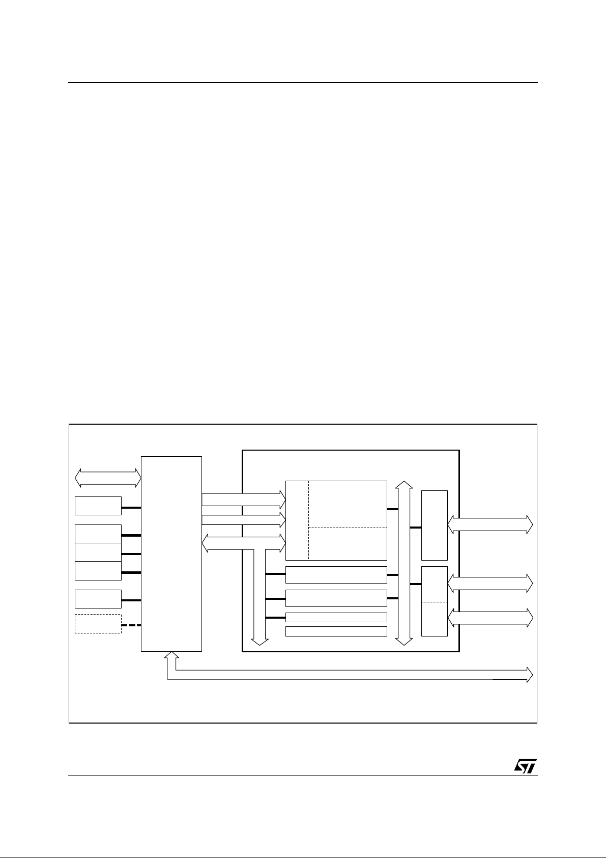
Figure 2. System Block Diagram, Two-C hip Solution
16 FLAGS
TIMER/
CAPTURE
SERIAL
DEVICE
SERIAL
DEVICE
SERIAL
DEVICE
UART
DEVICE
HOST
MCU
ANALOG
DEVICES
DSP
ADSP-2191
22 ADDRESS
WR, RD, BMS, MSx, IOMS
8 DATA
JTAG DEBUG
DSP SYSTEM MEMORY
LOGIC
ADDR & DECODE
16 MACROCELL PLD
POWER MANAGEMENT
CONTENT SECURITY
DSM2190F4
PRIMARY
FLA SH MEMORY
256K X 8
SECONDARY
FLA SH MEMORY
32K X 8
I/O CONTROL
8 I/O
I/O, PLD, CHIP SELECTS
PORTS
I/O BUS
8 I/O
PORTS
JTAG
ISP TO
ALL
AREAS
I/O, PLD, CHIP SEL
JTAG ISP
AI04959B
4/61

DSM2190F4
The two-chip combination of a D SP and a DSM
device is ideal for systems which have limitations
on size, EMI levels, and power consumption. DSM
memory and logic are “zero-power”, meaning they
automatically go to standby between memory accesses or logic input changes , producing low active and standby current consumption, which is
ideal for battery powered products.
Table 1. DSM2190F4V DSP Memory S ystem Devi ces
Secondar y
Flash
Memory
32KBytes =
4 sectors x
8KByte
32KBytes =
4 sectors x
8KByte
PLD
16
macro
-cells
16
macro
-cells
Part Number
DSM2190F4VV15T6
DSM2190F4VV15K6
Main Flash
Memory
256KBytes =
8 sectors x
32KByte
256KBytes =
8 sectors x
32KByte
Table 2. Compatible Analog Devices DSP
DSP Part Number
A programmable security bit in the DSM protects
its contents from unauthorized viewing and copying. When set, the security bit will block access of
programming devices (JTAG or others) to the
DSM Flash memories and PLD configuration. The
only way to defeat the security bit is to erase the
entire DSM device, after which the device is blank
and may be used again. The DSP will always have
access to Flash memory contents through the 8-bit
data port even while the security bit is set.
I/O
Ports
Up to
16
Up to
16
and I/O
V
CC
3.3V ±10% 150 ns
3.3V ±10% 150 ns
Operating Voltage, V
Mem
Speed
Package
52-pin
PQFP
52-pin
PLCC
CC
Operating
Temp
o
C to
–40
o
+85
o
C to
–40
o
+85
I/O Capability
C
C
ADSP-2191M 2.5V 2.5 - 3.6V
Figure 3. PLC C C onnection s Figure 4. PQFP C onnection s
RESET
PB7
CNTL2
CNTL0
CNTL1
PB0
PB1
PB2
PB3
PB4
PB5
GND
PB6
PB7
CNTL1
CNTL2
RESET
51
AD15
46
AD14
45
AD13
44
AD12
43
AD11
42
AD10
41
AD9
40
AD8
39
V
38
CC
AD7
37
AD6
36
AD5
35
AD4
34
PA0
AD2
AD1
AD3
AD0
AI02857
PD2
PD1
PD0
PC7
PC6
PC5
PC4
V
GND
PC3
PC2
PC1
PC0
CC
52515049484746454443424140
1
2
3
4
5
6
7
8
9
10
11
12
13
14151617181920212223242526
PA7
PA6
PA5
PA4
PA3
PA2
PA1
GND
47
48
49
50
CNTLO
39 AD15
38 AD14
37 AD13
36 AD12
35 AD11
34 AD10
33 AD9
32 AD8
31 V
CC
30 AD7
29 AD6
28 AD5
27 AD4
PA0
AD0
AD1
AD2
AD3
PD2
PD1
PD0
PC7
PC6
PC5
PC4
V
GND
PC3
PC2
PC1
PC0
PB0
PB1
PB2
PB3
PB4
PB5
GND
PB6
4
567
8
9
10
11
12
13
14
15
CC
16
17
18
19
20
21222324252627282930313233
PA7
PA6
PA5
PA4
52
2
3
1
PA3
PA2
PA1
GND
AI02858
5/61

DSM2190F4
ARCHITECTURAL OVERVIEW
Major functional blocks are shown in Figure 5.
DSP Address/Data/Control Interface
These DSP signals attach directly to the DSM for
a glueless connection. An 8-bit data connection is
formed and all 22 DSP address lines can be decoded as well as DSP memory strobes;
IOMS, and MSx. There are many different ways the
DSM2190F4 can be configured and used depending on system requirements. One convenient way
is to combine the function of t he
the
BMS signal. Doing this allows the DS P core t o
MSx signals into
access DSM memory at runtime even after the
boot process is complete using only the
nal. Comb ining
MSx and BMS consumes less I/O
pin(s) on the DMS device. See Analog Devices
ADSP-2191 DSP Hardware Reference Manual,
Chapter 7, Code Example: BMS Runtime Access.
Alternatively, any of the
MSx signals may also be
used to decode any of the sectors of DSM Main
Flash or Secondary flash memories.
Main Flash Memory
The 2M bit (256K x 8) Flash memory is divided into
eight equally-sized 32 K byte s ect ors t hat are i ndividually selectable through the Decode PLD. Each
Flash memory sector can be located at any address as defined by the user with PSDsoft Express. DSP code and data is easily placed in flash
memory using the P SDsoft Express software development tool.
Secondary Flash Memory
The 256K bit (32K x 8) Flash memory is divided
into eight equally-sized 8K byte sectors that are individually selectable through the Decode PLD.
Each Flash memory sector can be located at any
address as defined by the user with PSDsoft Express. DSP code and data can also be placed
Secondary Flash memory using the PSDsoft Express development tool.
Secondary flash memory is good for storing dat a
because of its small sectors. Additionally, software
EEPROM em ulation techniques can be used for
small data sets that change frequently on a byteby-byte basis.
Secondary flash may also be used to store custom
start-up code for applications that do not “boot” using DMA, but instead start executing code from external memory upon reset. Storing code here can
keep the entire Main Flash free of initialization
code for clean software partitioning. If only on e or
more 8K byte sectors are needed for start-up
code, the remaining sectors of Secondary Flash
may be used for data storage.
BMS,
BMS sig-
Secondary Flash may also be used as an extension to Main Flash memory producing a total of
288K bytes
Miscellaneous: Main and Secondary Flash memories are totally independent, allowing concurrent
operation if needed. The DSP can read from one
memory while erasing or programming the other.
The DSP can erase Flash memories by individual
sectors or the entire Flash memory array may be
erased at one time. Each sector in either Flash
memory may be individually write protected, blocking any writes from the DSP (good for boot and
start-up code protection). The Flash memories automatically go to standby between DSP read or
write accesses to conserve power. Maximum access times include sector decoding time. Maximum erase cycles is 100K and data retention is 15
years minimum. Flash memory, as well as the entire DSM device may be programmed with the
JTAG ISP interface with no DSP involvement.
Programm a b le Logic (PLD s)
The DSM family contains two PLDS that m ay optionally run in Turbo or Non-Turbo mode. PLDs operate faster (less propagation delay) while in
Turbo mode but consume more power than NonTurbo mode. Non-Turbo mode allows the PLDs to
automatically go to standby when no inputs are
change to conserve power. The Turbo mode setting is controlled at runtime by DSP software.
Decode PLD (DPLD). This is programmable logic used to select one of the eigh t individual Main
Flash memory segments, one of four individual
Secondary Flash memory segments, or the group
of control registers within the DSM device. The
DPLD can also optionally drive external chip select
signals on Port D pins. DPLD input signals include:
DSP address and control signals, Page Register
outputs, DSM Port Pins, CPLD logic feedback.
Complex PLD (CPLD). This programmable logic
is used to c reate bo th combinatorial and sequential general purpose logic. The C PLD contains 16
Output Macrocells (OMCs) and 16 Input Macrocells (IMCs). PSD Macrocell registers a re unique
in that that have direct connection to the DSP data
bus allowing them to be loaded and read directly
by the DSP at runtime. This di rect access is g ood
for making small peripheral devices (shifters,
counters, state machines, etc.) that are accessed
directly by the DSP with little overhead. DPLD inputs include DSP address and control signals,
Page Register outputs, DSM Port Pins, and CPLD
feedback.
6/61
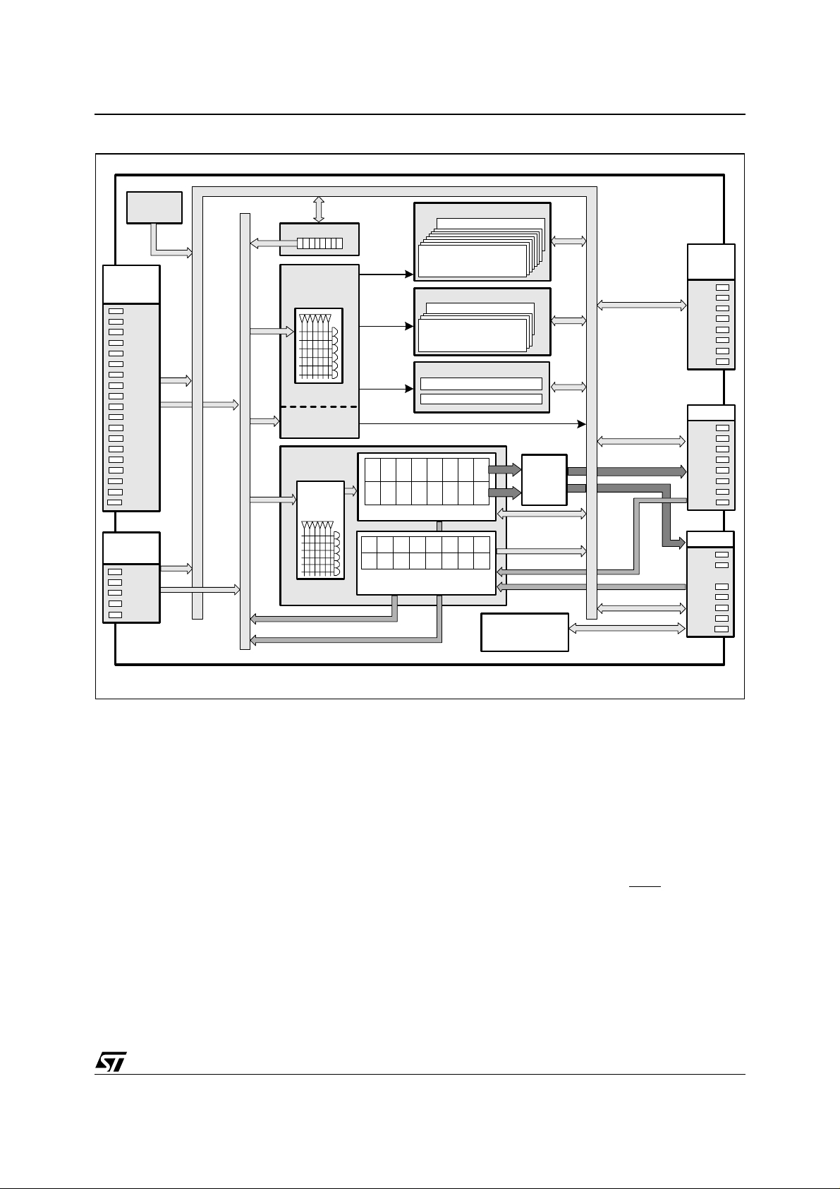
Figure 5. Block Diagram
DSM2190F4
SECURITY
LOCK
DSP
ADDR
AD0
AD1
AD2
AD3
AD4
AD5
AD6
AD7
AD8
AD9
AD10
AD11
AD12
AD13
AD14
AD15
PD0
PD1
PD2
DSP
CONTROL
CNTL0
CNTL1
CNTL2
PC2
RST\
INTERNAL ADDR, DATA, CONTROL BUS LINKED TO DSP
MAIN FLASH MEMORY
PAGE REG
DECODE PLD
(DPLD)
EXTERNAL
CHIP SELEC T S
COMPL EX PLD
PLD INPUT BUS
PIN FEEDBACK
NODE FEED BACK
(CPLD)
ARRAY
AND
FS0-7
CSBOOT0-3
CSIOP
EXTERNAL CHIP SELECTS, ESC0-2
ABA
B
BCBCBCBCBCBCBCB
16 Output Macrocells
BBB
CCCCBCBCBCBC
fs7
fs0
8 SEGMENTS, 32 KB
256 KBytes TOTAL
2nd FLASH MEMORY
csboot3
csboot0
4 SEGMEN T S, 8 KB
32 KBytes TOTAL
RUNTIME CONTROL
CSIOP REGISTER FILE
POWER MANAGEMENT
ABABABABABA
B
16 Input
Macrocell
B
C
JTAG-ISP
TO ALL AREAS
OF CHIP
ALLO-
CATOR
DSM2190F4
DSP SYS T EM
MEMORY
DSP
DATA
PA0
PA1
PA2
PA3
PA4
PA5
PA6
PA7
I/O PORT
PB0
PB1
PB2
PB3
PB4
PB5
PB6
PB7
I/O PORT
PC0
PC1
PC3
PC4
PC5
PC6
PC7
OMCs: The general structure of the CPLD is similar in nature to a 22V10 PLD device wit h t he familiar sum-of-products (AND-OR) construct. True
and compliment versions of 64 input signals are
available to a large AND array. AND array outputs
feed into a multiple product-term O R gate within
each OMC (up to 10 product-terms for each
OMC). Logic output of the OR gate can be passed
on as combinatorial logic or combined with a flipflop within in each OMC to realize sequential logic.
OMCs can be used a s a buried nodes with feedback to the AND array or OMC output can be routed to pins on Port B or PortC.
IMCs: Inputs from pins on Port B or Port C are
routed to IMCs for conditioning (clocking or latching) as they enter the chip, which is good for sampling and debouncing inputs. Alternatively, IMCs
can pass Port input signals directly to P LD inputs
without clocking or latching. The DSP may read
the IMCs at any time.
AI04960B
Runtime Control Registers
A block of 256 byt es is decoded inside the DSM
device as DSM control and status registers. 27
registers are used in the block of 256 locations to
control the output state of I/O pins, to read I/O
pins, to control p ower managem ent, to read /write
macrocells, and other functions at runtime. See
Table 4 for description. The base address of these
256 locations is referred to in this data sheet as
csiop
(Chip Select I/O Port). Individual registers
within this block are accessed with an offset from
csiop
the base address. The DSP accesses
ters using I/O memory with the
IOMS strobe.
regis-
csiop
registers are accessed as bytes.
Memory Page Register
This 8-bit register can be l oaded and read b y the
csiop
DSP at runtime as one of the
registers. Its
outputs feed directly into the PLDs. The page register can be used for special memory mapping requirements and also for general logic.
7/61

DSM2190F4
I/O Po r t s
The DSM has 19 individually configurable I/O pins
distributed over the three ports (Ports B, C, and D).
Each I/O pin can be individually configured for different functions such as standard MCU I/O p orts
or PLD I/O on a pin by pin basis. (MCU I/O means
that for each pin, its output state can be controlled
or its input value can be read by the DSP at runt-
csiop
ime using the
registers like an MCU would
do.)
Port C hosts the JTAG ISP signals. Sinc e JTAG-
ISP does not occur frequently during the life of a
product, those Port C pins are under-utilized. In
applications that need every I/O pin, JTAG signals
can be multiplexed with general I/O signals to use
them for I/O when not performing ISP. See section
titled “Programming In-Circuit using JTAG ISP” on
page 40 for muxing JTAG pins on Port C, and Application Note
The static configuration of all Port pins is d efined
with the PSDsoft Express
AN1153
.
TM
software development tool. The dynami c ac tion of th e P orts p ins is
controlled by DSP runtime software.
JTAG ISP Port
In-System Programming (ISP) can be pe rformed
through the JTAG signals on Port C. This serial interface allows programming of the entire DSM device or subsections (that is, only Flash memory but
not the PLDs) without the participation of the DSP.
A blank DSM device soldered to a circuit board
can be completely programmed i n 10 to 25 seconds. The basic JTAG signals; TMS, TCK, TDI,
and TDO form the IEEE-1149.1 interface. The
DSM device does not implement the IEEE-1149.1
Boundary Scan functions. The DSM uses the
JTAG interface for ISP only. However, the DSM
device can reside i n a standard JTAG chain with
other JTAG devices (including the ADSP-2191)
and it will remain in BYPASS mode while other devices perform Boundary Scan.
ISP programming time can be reduced as much as
30% by using two more signals on Port C, TSTAT
and TERR
in addition to TMS, TCK, TDI and TDO.
TM
The FlashLINK
JTAG programming cable is
available from STMicroelectronics for $59USD
and PSDsoft Express software is available at no
charge from
www.st.com/psm
. That is all that is
needed to program a DSM device using the parallel port on any PC or note-book. See section titled
“Programming In-Circuit using JTAG ISP” on page
40.
Power Management
csiop
The DSM has bits in
control registers that
are configured at run -time by the DSP to reduce
power consumption of the CPLD. The Turbo bit in
the PMMR0 register can be set to logic 1 and the
CPLD will go to Non-Turbo mode, meaning it will
latch its outputs and go to sleep until the next transition on its inputs. There is a slight penalty in PLD
performance (longer propagation delay), but significant power savings are realized.
Additionally, bits in two
csio p
registers can be set
by the DSP to selectively block signals from entering the CPLD which reduces power consumption.
See section titled “Power Management” on page
37.
Security and NVM Sector Protection
A programmable security bit in the DSM protects
its contents from unauthorized viewing and copying. When set, the security bit will block access of
programming devices (JTAG or others) to the
DSM Flash memory and PLD configuration. The
only way to defeat the security bit is to erase the
entire DSM device, after which the device is blank
and may be used again.
Additionally, the content s of ea ch in dividual F lash
memory sector can be write protected (sector protection) by configuration with PSDsoft Express
TM
This is typically used to protect DSP boot code
from being corrupted by inadvertent writes to
Flash memory from the DSP.
Pin Assign m ent s
Pin assignment are shown for the 52-pin PLCC
package in F igure 3, and the 5 2-pin PQFP package in Figure 4.
.
8/61
Table 3. Pin Description
Pin Name Type Description
ADIO0-15 In Sixteen address inputs from the DSP.
DSM2190F4
CNTL0 In Active low write strobe input (WR
CNTL1 In Active low read strobe input (RD
CNTL2 In Active low Byte Memory Select (BMS
Reset
PA0-7 I/O Eight data bus signals connected to DSP pins D8 - D15.
PB0-7 I/O
PC0-7 I/O
PD0-2 I/O
V
CC
GND Ground pins
Active low reset input from system. Resets DSM I/O Ports, Page Register contents, and other
In
DSM configuration registers. Must be logic Low at Power-up.
Eight configurable Port B signals with the following functions:
1. MCU I/O – DSP may write or read pins directly at runtime with csiop registers.
2. CPLD Output Macrocell (McellAB0-7 or McellBC0-7) outputs.
3. Inputs to the PLDs (Input Macrocells).
Note: Each of the four Port B signals PB0-PB3 may be configured at run-time as either standard
CMOS or for high slew rate. Each of the four Port B signals PB3-PB7 may be configured at
run-time as either standard CMOS or Open Drain Outputs.
Eight configurable Port C signals with the following functions:
1. MCU I/O – DSP may write or read pins directly at runtime with csiop registers.
2. CPLD Output Macrocell (McellBC0-7) output.
3. Input to the PLDs (Input Macrocells).
4. Pins PC0, PC1, PC5, and PC6 can optionally form the JTAG IEEE-1149.1 ISP serial
interface as signals TMS, TCK, TDI, and TDO respectively.
5. Pins PC3 and PC4 can optionally form the enhanced JTAG signals TSTAT and TERR
respectively. Reduces ISP programming time by up to 30% when used in addition to the
standard four JTAG signals: TDI, TDO, TMS, TCK.
6. Pin PC3 can optionally be configured as the Ready/Busy output to indicate Flash memory
programming status during parallel programming. May be polled by DSP or used as DSP
interrupt to indicate when Flash memory byte programming or erase operations are
complete.
Note 1: Port C pin PC2 input (or any PLD input pin) can be connected to the DSP IOMS
Note 2: When used as general I/O, each of the eight Port C signals may be configured at run-time
Note 3: The JTAG ISP pins may be multiplexed with other I/O functions.
Three configurable Port D signals with the following functions:
Note 1: Port D pin PD0 (or any PLD input pin) can be connected to the DSP A16 output. See
Note 2: Port D pin PD1 (or any PLD input pin) can be connected to the DSP A17 output. See
Note 3: Port D pin PD2 (or any PLD input pin) can be connected to the DSP A18 output. See
Supply Voltage
See Figure 6.
as either standard CMOS or Open Drain Outputs.
1. MCU I/O – DSP may write or read pins directly at runtime with csiop registers.
2. Input to the PLDs (no associated Input Macrocells, routes directly into PLDs).
3. CPLD output (External Chip Select). Does not consume Output Macrocells.
4. Pin PD1 can optionally be configured as CLKIN, a common clock input to PLD.
5. Pin PD2 can optionally be configured as CSI
memory. Flash memory is disabled to conserve more power when CSI
connect CSI
Figure 6
Figure 6.
Figure 6
to ADSP-218X PWDACK output signal.
) from the DSP
) from the DSP.
) signal from the DSP.
, an active low Chip Select Input to select Flash
output.
is logic high. Can
9/61

DSM2190F4
TYPICAL CONNECTIONS
Figure 6 shows a typical connection scheme.
Many connection possibilities exist since many
DSM pins are multipurpose. This scheme illustrates the use of a com bined function
(functions as
BMS and MSx), and many I/O pins. It
also illustrates how to chain the DSM and DSP devices together on the JTAG bus. The J TAG connector definition depends on development and
production environment requi reme nts. A s pe cially
defined connector can be devised to combine the
signals of the FlashLINK and the Analog Devices
emulator. Alternatively, two separate JTAG connectors can be used, one matching the pin out of
FlashLINK and the other matching the emulator pinout.
Keep in mind that signals
BMS, IOMS, MSx,
ADDR16, ADDR17, ADDR18 can be connected to
any DSM pin t hat is a PLD input. I /O pins on Po rt
B and Port C are m ore capable (more PLD functions) than Port D pins. It is recommended to use
Port D pins primarily for decode inputs first, leaving pins on Port B and Port C available for general
BSM signal
logic. Figure 6 illustrates a com mon way to m ake
connections.
Following are connection options to consider:
Port C JTAG: Figure 6 shows four JTAG signals
(TMS, TCK, TDI, TDO) connected to the DSM. Alternatively, using six-pin JTAG (two m ore signal s,
TSTAT and
TERR) can reduce ISP time by as
much as 30% compared to four-pin JTAG. Other
JTAG options include multiplexing JTAG pins with
general I/O (see “Programming In-Circuit using
JTAG ISP” on page 40 and Application Note
AN1153
), or not using J TAG at all. If no JTAG is
used, the DSM device has to be programmed on a
conventional programmer before it is installed on
the circuit board. Using no JTAG makes more
DSM I/O available.
Pins PC2 and PD2. If not all 288K a ddress locations need to be decoded in the DSM, then
ADDR18 on pin P D2 is n ot needed. In t his case,
IOMS signal can be connected to pin PD2, free-
the
ing pin PC2 for general I/O usage.
10/61
Figure 6. Typical Connections
DSM2190F4
DSM2190F4
PA0
PA1
PA2
PA3
PA4
I/O
PB0
PA5
I/O
PB1
PA6
I/O
PB2
PA7
I/O
I/O
PB3
PB4
CNTL0
I/O
CNTL1
I/O
PB6
PB5
CNTL2
PC2
I/O
PB7
CONNECTOR
DSM JTAG
VCC
JTAG_TDI
10k ohm
33 ohm
I/O
I/O
I/O
PC7
PC3
PC4
ADIO0
ADIO1
ADIO2
ADIO3
ADIO4
optional _TERR
optional TSTAT
TMS
TCK
TDI
TDO
PC1
PC0
PC6
PC5
ADIO5
ADIO6
ADIO7
ADIO8
ADIO9
ADIO10
ADIO11
ADIO12
ADIO13
ADIO14
ADIO15
PD1
PD2
PD0
_RESET
_RESET
DSP JTAG
JTAG_TMS
JTAG_TCK
JTAG_TDO
CONNECTOR
AI04961B
JTAG_TRST
EMULATOR STATUS
33 ohm
DATA1
DATA0
D0D1D2
_BR
BUS_REQUEST
DATA4
DATA2
DATA3
D3D4D5D6D7
ADSP-2191
_BG
_BGH
GRANT_HUNG
BUS_GRANT
DATA6
DATA5
CLKOUT
BYPASS
CLOCK OUT
PLL BYPASS
READ
WRITE
DATA7
I/O MEM SELECT
BOOT MEM SELECT
_RD
_WR
_MSx
_BMS
_IOM S
ADDR1
ADDR0
ADDR2
A0A1A2A3A4A5A6A7A8
ACK
ADDR4
ADDR6
ADDR8
ADDR10
ADDR3
ADDR5
ADDR7
ADDR13
ADDR9
ADDR11
ADDR12
ADDR14
ADDR15
ADDR16
ADDR17
ADDR18
RESET
A9
A12
A13
A14
A15
A18
A16
A10
A11
A17
_RESET
CLKIN
XTAL
PF1
PF2
PF3
PF0
I/O
I/O
I/O
I/O
I/O
XTAL
CLOCK or
PF8
PF9
PF6
PF10
PF7
PF4
PF5
I/O
I/O
I/O
PF11
PF12
PF13
PF14
PF15
SPORT0
SERIAL CHN
I/O
I/O
I/O
I/O
I/O
I/O
I/O
I/O
SERIAL
DEVICE
SPORT1
SERIAL CHN
DEVICE
SERIAL CHN
SERIAL
DEVICE
SPORT1
SERIAL
RxD, TxD
UART
DEVICE
JTAG TDI
TDI
JTAG TDO
TDO
TIMER/
JTAG TCK
TCK
TMR2-0
CAPTURE
JTAG _TRST
JTAG TMS
EMULATOR STATUS
TMS
_EMU
_TRST
BMODE0
BMODE1
OPMODE
Hx
HOST
PORT
11/61

DSM2190F4
TYPICAL MEMORY MAP
There many different ways to plac e (or map) the
addresses of DSM memory and I/O depending on
system requirements. The DP LD al lows com plete
mapping flexibility. Figure 7 shows one possible
system memory map. In this case, the DSP will
bootload (via DMA) the contents of Main Flash
memory upon reset. The Secondary Flash memory can be used for parameter storage or additional
code storage. BMS and MS x are conf igured in the
DSP to be combined into the
the DSP to access both Flash memories at runtime (after DMA boot). The DSP may execute code
BMS signal, allowing
directly from the DSM and well as erase and write
new code or data to DSM Flash.
The nomenclature
fs0..f s 7
are designators f or the
individual sectors of Main Flash memory, 32K
bytes each.
csboot0..csboot3
are designators for
the individual Secondary Flash memory segments, 8K bytes each.
csiop
designates the DSM
control register block.
The designer may easily specify memory mapping
in a point-and-click software environment using
PSDsoft Express
TM
.
12/61
Figure 7. Typ ic a l Sy st em Mem ory Map
DSM2190F4
56000-57FFF
54000-55FFF
52000-53FFF
50000-51FFF
4FFFF
48000
47FFF
40000
3FFFF
38000
37FFF
30000
2FFFF
28000
27FFF
20000
1FFFF
18000
17FFF
10000
DSP Boot Memory
Space (BMS)
csboot
, 8KB 2nd Flash
csboot
, 8KB 2nd Flash
csboot
, 8KB 2nd Flash
csboot
, 8KB 2nd Flash
fs7
32K bytes Main Flash
fs6
32K bytes Main Flash
fs5
32K bytes Main Flash
fs4
32K bytes Main Flash
fs3
32K bytes Main Flash
fs2
32K bytes Main Flash
fs1
32K bytes Main Flash
fs0
32K bytes Main Flash
DSP I/O Memor y
Space (IOMS)
csiop
256 CONTROL REGS
02000-020FF
AI04962
13/61
DSM2190F4
SPECIFYING THE MEMORY MAP WITH PSDSOFT EXPRESS
The memory map shown in Figure 7 can be easily
implemented using PSDsoft Express
and-click environment. PSDsoft Express
TM
in a point-
TM
will
statemen ts of the ABEL language. Figure 8 shows
the resulting equations generated by PSDsoft ExpressTM.
TM
generate Hardware Definition Language (HDL)
Figure 8. HDL Statements Generated from PSDsoft Express to Implement Memory M ap
csiop = ((address >= ^h2000) & (address <= ^h20FF) & (!_ioms));
fs0 = ((address >= ^h10000) & (address <= ^h17FFF) & (!_bms));
fs1 = ((address >= ^h18000) & (address <= ^h1FFFF) & (!_bms));
fs2 = ((address >= ^h20000) & (address <= ^h27FFF) & (!_bms));
fs3 = ((address >= ^h28000) & (address <= ^h2FFFF) & (!_bms));
fs4 = ((address >= ^h30000) & (address <= ^h37FFF) & (!_bms));
fs5 = ((address >= ^h38000) & (address <= ^h3FFFF) & (!_bms));
fs6 = ((address >= ^h40000) & (address <= ^h47FFF) & (!_bms));
fs7 = ((address >= ^h48000) & (address <= ^h4FFFF) & (!_bms));
csboot0 = ((address >= ^h50000) & (address <= ^h51FFF) & (!_bms));
csboot1 = ((address >= ^h52000) & (address <= ^h53FFF) & (!_bms));
csboot2 = ((address >= ^h54000) & (address <= ^h55FFF) & (!_bms));
csboot3 = ((address >= ^h56000) & (address <= ^h57FFF) & (!_bms));
Specifying these equations using PSDsoft Ex-
TM
press
is very simple. Figure 9 shows how to
specify the equation for the 32K Byt e Fl ash mem-
fs2
ory se gment,
. Notice
fs2
is qualified with the
signals
BMS. This specif ication proces s is repeat-
ed for all other Flash memory segments, the
register block, and any external chip select signals
that may be needed (ADC, etc.).
csiop
Figure 9. PSDsoft Express
TM
Memory Mapping
14/61
RUNTIME CONTROL REGISTER DEFINITION
There are up to 256 addresses decoded inside the
DSM device for control and status information. 27
of these locations contain registers that the DSP
can access at runtime. The base address of this
block of 256 locations is referred to in this manual
as
csiop
(Chip Select I/O Port). Table 4 lists the 27
registers and their offsets (in hexadecimal) from
csiop
the
base address needed t o acc ess in dividual DSM control and status registers. The DSP will
access these registers in I/O memory space using
DSM2190F4
its
IOMS strobe. These regis ters are accesses in
bytes, so the DSP should ignore the upper byte of
its 16-bit I/O access.
Note1: All
reset.
Note2: Do not write to unused locations within the
csiop
logic zero.
csiop
registers are cleared to logic 0 at
block of 256 registers. They should remain
Table 4.
Data In 01 10 11
Data Out 05 12 13
Direction 07 14 15
Drive Select 09 16 17
Input Macrocells 0B 18 Read to obtain state of IMCs. No writes.
Enable Out 0D 1A 1B
Output Macrocells AB 20
Output Macrocells BC 21
Mask Macrocells AB 22
Mask Macrocells BC 23
CSIOP
Register Name Port B P ort C Port D Other Description
Registers and their Offsets (in hexadecimal)
MCUI/O input mode. Read to obtain current logic level of
Port pins. No writes.
MCU I/O output mode. Write to set logic level on Port
pins. Read to check status.
MCU I/O mode. Configures Port pin as input or output.
Write to set direction of Port pins.
Logic 1 = out, Logic 0 = in. Read to check status.
Write to configure Port pins as either standard CMOS or
Open Drain on some pins, while selecting high slew rate
on other pins. Read to check status.
Read to obtain the status of the output enable logic on
each I/O Port driver. No writes.
Read to get logic state of output of OMC bank AB.
Write to load registers of OMC bank AB.
Read to get logic state of output of OMC bank BC.
Write to load registers of OMC bank BC.
Write to set mask for loading OMCs in bank AB. A logic
1 in a bit position will block reads/writes of the
corresponding OMC. A logic 0 will pass OMC value.
Read to check status.
Write to set mask for loading OMCs in bank BC. A logic
1 in a bit position will block reads/writes of the
corresponding OMC. A logic 0 will pass OMC value.
Read to check status.
Main Flash Sector
Protection
Security Bit and
Secondary Flash
Sector Protection
JTAG Enable C7
PMMR0 B0 Power Management Register 0. Write and read.
PMMR2 B4 Power Management Register 2. Write and read.
Page E0 Memory Page Register. Write and read.
Read to determine Main Flash Sector Protection
C0
Setting. No writes.
Read to determine if DSM devices Security Bit is active.
Logic 1 = device secured.
C2
Also read to determine Secondary Flash Protection
Setting status. No Writes.
Write to enable JTAG Pins (optional feature). Read to
check status.
15/61

DSM2190F4
DETAILED OPERATION
Figure 5 shows major functional areas of the device :
■ Flash Memories
■ PLDs (DPLD, CPLD, Page Register)
■ DSP Bus Interface (Address, Data, Control)
■ I/O Por ts
■ Runtime Control Registers
■ JTAG ISP Interface
The following describes these functions in more
detail.
Flash Memories
The Main Flash memory array is divided into eight
equal 32K byte sectors. The Secondary Flash
memory array is divided into four equ al 8K byte
sectors. Each sector is selected by the DPLD can
be separately protected from program and erase
cycles. This configuration is specified by using PSDsoft Express
Memory Sector Select Signals. The DPLD generates the Select signals for all the internal memory blocks (see Figure 14). Each of the twelve
sectors of the Flash mem ories has a sel ec t signal
FS0-FS7, or CSBOOT0-CSBOOT3
(
tains up to three product terms. Having t hree product terms for each select signal allows a given
sector to be mapped into multiple ar e as of system
memory if needed.
Ready/Busy
output the Ready/
output on Ready/
Flash memory array is being written,
ther Flash memory array is being erased. The output is a 1 (Ready) wh en no Write o r Erase cycle is
TM
.
) which con-
(PC3 ). This signal can be used to
Busy status of the device. The
Busy is a 0 (Busy) when either
or
when ei-
in progress. This signal may be polled by the DSP
or used as a DSP interrupt to indicate when an
erase or program cycle is complete.
Memory Operation. The Flash memories are accessed through the DSP Address, Data, and Control Bus Interface.
DSPs and MCUs cannot write to Flash memory as
it would an SRAM device. Flash memory must first
be “unlocked” with a special sequence of byte
write operations to invoke an internal algorithm,
then a single data byte is written to the Flash memory array, then programming status is chec ked by
a byte read operation or by checking the Ready/
Busy pin (PC3). Table 5 lists all of the special in-
struction sequences to program (write) data to the
Flash memory arrays, erase the arrays, and check
for different types of status from the arrays. These
instruction sequences are different combinations
of individual byte write and byte read operations.
IMPORTANT: The DSP may not read and execute
code from the same Flash memory array for which
it is directing an instruction sequence. Or more
simply stated, the DSP may not read code the
same Flash array that is writing or erasing. Instead, the DSP must execute code from an alternate memory (like its own internal SRAM or a
different Flash array) while sending instructions to
a given Flash array. Since the two Flash memory
arrays inside the DSM device are completely independent, the DSP may read code from one array
while sending instructions to the other.
After a Flash memo ry array is programmed (written) it will go to “Read Array” mo de, then th e DSP
can read from Flash mem ory just as if would from
any 8-bit ROM or SRAM device.
16/61

DSM2190F4
Table 5. Instruction Sequences
Instruction
Sequence
Cycle 1 Cycle 2 Cycle 3 Cycle 4 Cycle 5 Cycle 6 Cycle 7
1,2,3,4
Read byte
Read Memory
Contents
5
from any
valid Flash
memory addr
Read Flash
Identifier (Main
Flash only)
6,7
Read Memory
Sector Protection
6,7,8
Status
Program a Flash
Byte
Flash Bulk Erase
Flash Sector
10
Erase
Write AAh to
XX555h
Write AAh to
XX555h
Write AAh to
XX555h
Write AAh to
9
XX555h
Write AAh to
XX555h
Write 55h
to XXAAAh
Write 55h
to XXAAAh
Write 55h
to XXAAAh
Write 55h
to XXAAAh
Write 55h
to XXAAAh
Write 90h
to XX555h
Write 90h
to XX555h
Write A0h
to XX555h
Write 80h
to XX555h
Write 80h
to XX555h
Read identifier
with addr lines
A6,A1,A0 =
0,0,1
Read identifier
with addr lines
A6,A1,A0 =
0,1,0
Write
(program)
data to addr
Write AAh to
XX555h
Write AAh to
XX555h
Write 55h
to XXAAAh
Write 55h
to XXAAAh
Write 10h
to XX555h
Write 30h
to another
Sector
Write 30h
to another
Sector
Write B0h to
Suspend Sector
11
Erase
address that
activates any
of FS0 - FS7
Write 30h to
Resume Sector
12
Erase
addr that
activates any
of FS0 - FS7
Write F0h to
Reset Flash
6
address that
activates any
of FS0 - FS7
Note: 1. All val ues are in hexadecimal, X = Don’t Care
2. A d esired int ernal Flash memory sec tor select signal (FS0 - F S 7 or CSBOO T 0 - CSBOOT3 ) m ust be acti ve for each write or read
cycle. Only one of these sector select signals will be active at any given time depending on the address presented by the DSP and
the memory mapping defi ned in PSDs oft Express. FS0 - FS7 and CSBOOT0- CS BOOT3 are act i ve high logic internal l y.
3. DS P addres ses A18 thr ough A12 ar e Don’t Care during t he instruc tion sequ ence de coding . Only addre ss bits A 11-A0 are used
during Fl ash memo ry instructio n sequence decoding b us cycles . The individ ual sector select sign al (FS0 - F S7 or CSB OOT0CSBOOT3) which is active during the instruction sequences determines the complete address.
4. For write operations, addresses are latched on the falling edge of Write Strobe (WR
Write Strobe (WR
5. No Unlock or In st ruction cycl es are required when the device is in the Read Arr ay mode. Operation is like reading a ROM device.
6. The Reset Flash instruction is required to return to the normal Read Array mode if the Error Flag (DQ5) bit goes High, or after reading the Flash I dentifier or after read i ng t he Sector Protection Status.
7. The DSP cannot invoke this instruction sequence while executing code from the same Flash memory as that for which the instruction sequence is intended. The DSP must fetch, for example, the code from the DSP SRAM when reading the Flash memory Identifier or Sector Protection Status.
8. The da ta is 00h for an unprote cted sector, and 01h for a pr otected sec tor. In the fo urth cycle, th e Sector Sele ct is active, and
(A1,A0)= (1,0)
9. Di recting this comma nd to any in dividua l active Flash memory seg ment (FS 0 - FS7) will invoke th e bulk era se of all eight Flash
memory sectors.
10. DS P wr ites c omma nd s eque n ce t o init ial s egme nt t o be erase d, t hen wr ite s the byte 30h to ad diti onal sect ors to b e er ased . Th e
byte 30h must be addressed to one of the other Flash memory segments (FS0 - FS7) for each additional segment (write 30h to any
address within a desir ed sector). No more than 80uS can elaps e between su bsequent additional sector erase commands .
11. The s y stem ma y perfo rm R ead an d P rogra m c ycl es in n on- erasi ng s ecto rs, read t he Flas h ID o r read t he Se ctor Protec t S tatu s,
when in the Suspend Sector Erase mode. The Suspend Sector Erase instruction sequence is valid only during a Sector Erase cycle.
12. The Resume Sector Erase instru ction sequence is valid only during the Suspend Sector Erase mode.
, CNTL0)
, CNTL0), Dat a i s latched on the risin g e dge of
17/61

DSM2190F4
Instruction Sequences
An instruction sequence consists of a sequence of
specific write or read operations. Each byte written
to the device is received and sequentially decoded
and not executed as a standard write operation to
the memory array. The instruction sequence is executed when the correct number of bytes are properly received and the time between two
consecutive bytes is shorter than the time-out period. Some instruction sequences are structured to
include read operations after the initial write operations.
The instruction sequence must be followed exac tly. Any in valid com binatio n of ins truction bytes o r
time-out between two consecutive bytes while addressing Flash memory resets the device logic into
Read Array mode (Flash memory is read like a
ROM device). The device s upports the instruction
sequences summarized in Table 5:
Flash memory:
■ Erase memory by chip or sector
■ Suspend or resume sector erase
■ Program a Byte
■ Reset to Read Array mode
■ Read primary Flash Identifier value
■ Read Sector Protection Status
These instruction sequences are detailed in Table
5. For efficient decoding of the instruction sequences, the first two bytes of an i nstruction sequence are the coded cycles and are followed by
an instruction byte or confirmation byte. The coded
cycles consist of writing the data AAh to address
XX555h during the first cycle and data 55h to address XXAAAh during the second cycle. Address
signals A18-A12 are Don’t Care during the instruction sequence Write cycles. However, the appropriate internal Sector Select (
CSBOOT0-CSBOOT3
) must be selected internal-
FS0-FS7 or
ly (active, which is logic 1).
Reading Flash Memory
Under typical conditions, the D SP may read the
Flash memory using read operations just as it
would a ROM or RAM device. Alternately, the DSP
may use read operations to obtain status information about a Program or Erase cycle that is currently in progress. Lastly, the DSP may use
instruction sequences to read special data from
these memory blocks. The following sections describe these read instruction sequences.
Read Memory Contents. Flash memory is
placed in the Read Array mode after Power-up,
chip reset, or a Reset Flash memory instruction
sequence (see Table 5). The DSP can read the
memory contents of the Flash memory by using
read operations any time the read operation is not
part of an instruction sequence.
Read Main Flash Identifier. The Main Flash
memory identifier is read with an instruction sequence composed of 4 operations: 3 specific write
operations and a read operation (see Table 5).
During the read operation, address bits A6, A1,
and A0 must be 0,0,1, respectively, and the appropriate internal Sector Select (
FS0-FS7
) must be
active. The identifier is 0xE7. Not Applicable to
Secondary Flash.
Read Memory Sector Protection Status. The
Flash memory Sector Protection Status is read
with an instruction sequence composed of 4 operations: 3 specific write operations and a read operation (see Table 5). During the read operation,
address bits A6, A1, and A0 must be 0,1,0, respectively, while internal Sector Sele ct (FS0-FS7
or CSBOOT0-CSBOOT3) designates the Flash
memory sector whose protection has to be verified. The read operation produces 01h if the Flash
memory sector is protected, or 00h if th e sector is
not protected.
The sector protection status can also be read by
the DSP accessing the Flash memory Prot ection
csiop
registers in
space. See the section ent itled
“Flash Memory Sector Protect” for register definitions .
Table 6. Status Bit Definition
Functional Block
Flash Memory
Note: 1. X = Not guaranteed value, can be rea d ei t her 1 or 0.
2. DQ7-DQ0 represent the Data Bus bits, D7-D0.
FS0-FS7, or
CSBOOT0-CSBOOT3
Active (the desired
segment is selected)
DQ7 DQ6 DQ5 DQ4 DQ3 DQ2 DQ1 DQ0
Data
Polling
Reading the Erase/Program Status Bits. The
device provides several status bits to be used by
the DSP to confirm the completion of an Erase or
18/61
Toggle
Flag
Error
Flag
Erase
X
Time-
out
XXX
Program cycle of Flash memory. These st atus bits
minimize the time that the DSP spends performing
these tasks and are defined in Table 6. The status
bits can be read as many times as needed.

DSM2190F4
For Flash memory, the DS P can perform a read
operation to obtain these status bits while an
Erase or Program instruction sequence is being
executed by the embedded algorithm. See the
section entitled “Programming Flash Memory”, on
page 19, for details.
Data Polling Flag (DQ7). When erasing or programming in Flash memory, the Data Polling Flag
(DQ7) bit outputs the co mplem ent of the bit bei ng
entered for programming/writing on the Data P olling Flag (DQ7) bit. Once the Program instruction
sequence or the write operation is c ompleted, t he
true logic value is read on the Data Polling Flag
(DQ7) bit (in a read operation).
Flash memory instruction features.
■ Data Polling is effective after the fourth Write
pulse (for a Program instruction sequence) or
after the sixth Write pulse (for an Erase
instruction sequence). It must be performed at
the address being programmed or at an address
within the Flash memory sector being erased.
■ During an Erase cycle, the Data Polling Flag
(DQ7) bit outputs a 0. After completion of the
cycle, the Data Polling Flag (DQ7) bit outputs
the last bit programmed (it is a 1 after erasing).
■ If the byte to be programmed is in a protected
Flash memory sector, the instruction sequence
is ignored.
■ If all the Flash memory sectors to be erased are
protected, the Data Polling Flag (DQ7) bit is
reset to 0 for about 100 µs, and then returns to
the previous addressed byte. No erasure is
performed.
Toggle Flag ( DQ6 ). The device offers another
way for determining when t he F lash memory Program cycle is completed. During the in ternal write
operation and when the Sector Select FS0-FS7 (or
CSBOOT0-CSBOOT3) is true, the Toggle Flag
(DQ6) bit toggles from 0 to 1 and 1 to 0 on subsequent attempts to read any byte of the memory.
When the internal cycle is complete, the toggling
stops and the data read on the Data Bus D0-7 is
the addressed mem ory byte. The device is now
accessible for a new read or write operation. The
cycle is finished when two successive reads yield
the same output data. Flash m emo ry spe cific features:
■ The Toggle Flag (DQ6) bit is effective after the
fourth write operation (for a Program instruction
sequence) or after the sixth write operation (for
an Erase instruction sequence).
■ If the byte to be programmed belongs to a
protected Flash memory sector, the instruction
sequence is ignored.
■ If all the Flash memory sectors selected for
erasure are protected, the Toggle Flag (DQ6) bit
toggles to 0 for about 100 µs and then returns to
the previous addressed byte.
Error Flag (DQ5). During a normal Program or
Erase cycle, the Error Flag (DQ5) bit is to 0. T his
bit is set to 1 when there is a failure during Flash
memory Byte Program, Sector Erase, or Bulk
Erase cycle.
In the case of Flash memory programming, the Error Flag (DQ5) bit indicates the attempt to program
a Flash memory bit from the programmed state, 0,
to the erased state, 1, whi ch is not vali d. The Error
Flag (DQ5) bit may also indicate a Time-out condition while attempting to program a byte.
In case of an error in a Flash memory Sector Erase
or Byte Progra m cycle, the Fl ash memory sector i n
which the error occurred or to which the programmed byte belongs must no longer be used.
Other Flash memory sectors may still be used.
The Error Flag (DQ5) bit is reset after a Reset
Flash instruction sequence.
Erase Time-out Flag (DQ3). The Erase Timeout Flag (DQ3) bit reflects the time-out period allowed between two consecutive Sec tor Erase instruction sequence bytes. The Erase Time-out
Flag (DQ3) bit is reset to 0 after a Sector Erase cycle for a time period of 100 µs + 20% unless an additional Sector Erase instruction sequence is
decoded. After this time period, or when the additional Sector Erase instruction sequence is decoded, the Erase Time-out Flag (DQ3) bit is set to 1.
Programming Flash Memory
When a byte of Flash memory is programmed, individual bits a re p ro grammed to logic 0. You cannot program a bit in Flash memory to a logic 1
once it has b een programmed to a logic 0. A bit
must be erased to logic 1, and programmed to logic 0. That means Flash memory must be erased
prior to being programmed. A b yte o f Flash memory is erased to all 1s (FFh). The DSP may erase
the entire Flash memory array all at once or individual sector-by-sector, but not byte-by-byte.
However, the DSP may program Flash memory
byte-by-byte.
The Flash memory requires the DSP to send an instruction sequence to program a byte or to erase
sectors (see Table 5).
Once the DSP issues a Flash memory Program or
Erase instruction sequence, it must check for the
status bits for completion. The embedded algorithms that are invoked inside the device provide
several ways give status to the DSP. Status may
19/61
 Loading...