

DSM (Digital Signal Processor System Memory)
For Analog Devices ADSP-218X Family (5V Supply)
FEATURES SUMMARY
■ Glueless Connection to DSP
– Easily add memory, logic, and I/O to DSP
■ 128K Byte Flash Memory
– For Bootloading and/or Data Overlay Memory
– Programmable Decoding and Paging Logic
allows accessing Flash memory as Byte DMA
(BDMA) and as External Da ta Overlay memory
– Rapid ly acc ess F lash memory with BDMA f o r
booting and loading internal DSP Overlay
memory. Alternati vely access t he same Flash
memory a s Exte rn al Data Over la y memo ry to
efficiently write Flash memory with code updates and data, a byte at a time with no DMA
setup overhead
– Individual 16K Byte Flash memory sectors
match size of DSP External Data Overlay
window for efficient data management. Integrated page logic provides easy DSP access
to all 128K Bytes.
– DSM connects to lower byte of 16-bit DSP
data bus. Byte-wide acc esses to 8-bi t B DMA
space. Half-word accesses to 16-bit Data
Memory Overlay and 16-bit I/O Mem space.
■ 5V Devices (±10%)
■ Up to 16 Multifunction I/O Pins
– Increase total DSP system I/O capability
– I/O controlled by DSP software or PLD logic
– 8mA I/O pin drive at 5 Vcc
■ Genera l pu rpo s e P LD
– Over 3,000 Gates of PLD with 16 macro cells
– Use for peripheral glue logic to keypads, con-
trol panel, displays, LCD, UART devices, etc.
– Eliminate PLDs and external logic devices
– Create state machines, chip selects, simp le
shifters and counters, clock dividers, delays
– Simple PSDsoft Express
TM
software ...Free
DSM2180F3
Figure 1. Packages
PQFP52 (T)
PLCC52 (K)
■ In-System Programming (ISP) with JTAG
– Program entire chip in 10-20 seconds with no
involvement of the DSP
– Eliminate sockets for pre-programm ed me m-
ory and logic devices
– Efficient manufacturing allows easy product
testing and Just-In-Time inventory
CC
TM
cable with PC
=5V
– Use low-cost FlashLINK
■ Content Security
– Programmable Security Bit blocks access of
device programmers and readers
■ Zero-Power Techno lo gy
–75 µA standby at V
■ Small Packaging
– 52-pin PQFP or 52-pin PLCC
■ Memory Spee d
–90 ns
1/63December 2001

DSM2180F3
TABLE OF CONTENTS
Summary Description . . . . . . . . . . . . . . . . . . . . . . . . . . . . . . . . . . . . . . . . . . . . . . . . . . . . . . . . . . . . . . 4
Architectural Overview . . . . . . . . . . . . . . . . . . . . . . . . . . . . . . . . . . . . . . . . . . . . . . . . . . . . . . . . . . . . . 7
DSP Address/Data/Control Interface. . . . . . . . . . . . . . . . . . . . . . . . . . . . . . . . . . . . . . . . . . . . . . . . . 7
Flash Memory . . . . . . . . . . . . . . . . . . . . . . . . . . . . . . . . . . . . . . . . . . . . . . . . . . . . . . . . . . . . . . . . . . 7
Programmable Logic (PLDs). . . . . . . . . . . . . . . . . . . . . . . . . . . . . . . . . . . . . . . . . . . . . . . . . . . . . . . 8
Runtime Control Registers . . . . . . . . . . . . . . . . . . . . . . . . . . . . . . . . . . . . . . . . . . . . . . . . . . . . . . . . 9
Memory Page Register . . . . . . . . . . . . . . . . . . . . . . . . . . . . . . . . . . . . . . . . . . . . . . . . . . . . . . . . . . . 9
I/O Ports . . . . . . . . . . . . . . . . . . . . . . . . . . . . . . . . . . . . . . . . . . . . . . . . . . . . . . . . . . . . . . . . . . . . . . 9
JTAG ISP Port. . . . . . . . . . . . . . . . . . . . . . . . . . . . . . . . . . . . . . . . . . . . . . . . . . . . . . . . . . . . . . . . . . 9
Power Management . . . . . . . . . . . . . . . . . . . . . . . . . . . . . . . . . . . . . . . . . . . . . . . . . . . . . . . . . . . . . 9
Security and NVM Sector Protection. . . . . . . . . . . . . . . . . . . . . . . . . . . . . . . . . . . . . . . . . . . . . . . . . 9
Pin Assignments . . . . . . . . . . . . . . . . . . . . . . . . . . . . . . . . . . . . . . . . . . . . . . . . . . . . . . . . . . . . . . . . 9
Typical connections . . . . . . . . . . . . . . . . . . . . . . . . . . . . . . . . . . . . . . . . . . . . . . . . . . . . . . . . . . . . . . 11
Memory Map. . . . . . . . . . . . . . . . . . . . . . . . . . . . . . . . . . . . . . . . . . . . . . . . . . . . . . . . . . . . . . . . . . . . . 13
Specifying Mem Map with PSDsoft ExpressTM . . . . . . . . . . . . . . . . . . . . . . . . . . . . . . . . . . . . . . . . 15
Runtime control register definition . . . . . . . . . . . . . . . . . . . . . . . . . . . . . . . . . . . . . . . . . . . . . . . . . . 17
Detailed Operation. . . . . . . . . . . . . . . . . . . . . . . . . . . . . . . . . . . . . . . . . . . . . . . . . . . . . . . . . . . . . . . . 18
Flash Memory . . . . . . . . . . . . . . . . . . . . . . . . . . . . . . . . . . . . . . . . . . . . . . . . . . . . . . . . . . . . . . . . . 18
Instruction Sequences. . . . . . . . . . . . . . . . . . . . . . . . . . . . . . . . . . . . . . . . . . . . . . . . . . . . . . . . . . . 2 0
Reading Flash Memory . . . . . . . . . . . . . . . . . . . . . . . . . . . . . . . . . . . . . . . . . . . . . . . . . . . . . . . . . . 2 0
Programming Flash Memory. . . . . . . . . . . . . . . . . . . . . . . . . . . . . . . . . . . . . . . . . . . . . . . . . . . . . . 21
Erasing Flash Memory. . . . . . . . . . . . . . . . . . . . . . . . . . . . . . . . . . . . . . . . . . . . . . . . . . . . . . . . . . . 23
Flash Memory Sector Protect.. . . . . . . . . . . . . . . . . . . . . . . . . . . . . . . . . . . . . . . . . . . . . . . . . . . . . 24
DSM Security Bit . . . . . . . . . . . . . . . . . . . . . . . . . . . . . . . . . . . . . . . . . . . . . . . . . . . . . . . . . . . . . . . 25
Reset Flash . . . . . . . . . . . . . . . . . . . . . . . . . . . . . . . . . . . . . . . . . . . . . . . . . . . . . . . . . . . . . . . . . . . 25
Page Register . . . . . . . . . . . . . . . . . . . . . . . . . . . . . . . . . . . . . . . . . . . . . . . . . . . . . . . . . . . . . . . . . 25
PLDs . . . . . . . . . . . . . . . . . . . . . . . . . . . . . . . . . . . . . . . . . . . . . . . . . . . . . . . . . . . . . . . . . . . . . . . . 25
Decode PLD (DPLD). . . . . . . . . . . . . . . . . . . . . . . . . . . . . . . . . . . . . . . . . . . . . . . . . . . . . . . . . . . . . . . 27
Complex PLD (CPLD) . . . . . . . . . . . . . . . . . . . . . . . . . . . . . . . . . . . . . . . . . . . . . . . . . . . . . . . . . . . . . 28
2/63

DSM2180F3
DSP Bus Interface. . . . . . . . . . . . . . . . . . . . . . . . . . . . . . . . . . . . . . . . . . . . . . . . . . . . . . . . . . . . . . 32
I/O Ports . . . . . . . . . . . . . . . . . . . . . . . . . . . . . . . . . . . . . . . . . . . . . . . . . . . . . . . . . . . . . . . . . . . . . 32
Port Operating Modes . . . . . . . . . . . . . . . . . . . . . . . . . . . . . . . . . . . . . . . . . . . . . . . . . . . . . . . . . . . 33
Port B – Functionality and Structure . . . . . . . . . . . . . . . . . . . . . . . . . . . . . . . . . . . . . . . . . . . . . . . . 35
Port C – Functionality and Structure . . . . . . . . . . . . . . . . . . . . . . . . . . . . . . . . . . . . . . . . . . . . . . . . 36
Port D – Functionality and Structure . . . . . . . . . . . . . . . . . . . . . . . . . . . . . . . . . . . . . . . . . . . . . . . . 37
Power Management. . . . . . . . . . . . . . . . . . . . . . . . . . . . . . . . . . . . . . . . . . . . . . . . . . . . . . . . . . . . . . . 39
PLD Power Management . . . . . . . . . . . . . . . . . . . . . . . . . . . . . . . . . . . . . . . . . . . . . . . . . . . . . . . . 4 0
PSD Chip Select Input (CSI, PD2) . . . . . . . . . . . . . . . . . . . . . . . . . . . . . . . . . . . . . . . . . . . . . . . . . 40
Power On Reset, Warm Reset, Power-down . . . . . . . . . . . . . . . . . . . . . . . . . . . . . . . . . . . . . . . . . 41
Programming In-Circuit using JTAG ISP. . . . . . . . . . . . . . . . . . . . . . . . . . . . . . . . . . . . . . . . . . . . . 41
AC/DC Parameters. . . . . . . . . . . . . . . . . . . . . . . . . . . . . . . . . . . . . . . . . . . . . . . . . . . . . . . . . . . . . . . . 44
Table: Absolute Maximum Ratings. . . . . . . . . . . . . . . . . . . . . . . . . . . . . . . . . . . . . . . . . . . . . . . . .45
Table: Operating Conditions. . . . . . . . . . . . . . . . . . . . . . . . . . . . . . . . . . . . . . . . . . . . . . . . . . . . . . 46
Table: DC Characteristics. . . . . . . . . . . . . . . . . . . . . . . . . . . . . . . . . . . . . . . . . . . . . . . . . . . . . . . . 48
Table: CPLD Combinatorial Timing . . . . . . . . . . . . . . . . . . . . . . . . . . . . . . . . . . . . . . . . . . . . . . . .49
Table: CPLD Macrocell Synchronous Clock Mode Timing. . . . . . . . . . . . . . . . . . . . . . . . . . . . . . . 50
Table: CPLD Macrocell Asynchronous Clock Mode Timing. . . . . . . . . . . . . . . . . . . . . . . . . . . . . . 50
Table: Input Macrocell Timing . . . . . . . . . . . . . . . . . . . . . . . . . . . . . . . . . . . . . . . . . . . . . . . . . . . . 52
Table: Read Timing . . . . . . . . . . . . . . . . . . . . . . . . . . . . . . . . . . . . . . . . . . . . . . . . . . . . . . . . . . . . 53
Table: Write Timing . . . . . . . . . . . . . . . . . . . . . . . . . . . . . . . . . . . . . . . . . . . . . . . . . . . . . . . . . . . . 54
Table: Flash Memory Program, Write and Erase Times . . . . . . . . . . . . . . . . . . . . . . . . . . . . . . . . 55
Table: Reset (Reset) Timing. . . . . . . . . . . . . . . . . . . . . . . . . . . . . . . . . . . . . . . . . . . . . . . . . . . . . . 5 5
Table: ISC Timing. . . . . . . . . . . . . . . . . . . . . . . . . . . . . . . . . . . . . . . . . . . . . . . . . . . . . . . . . . . . . . 56
PACKAGE MECHANICAL . . . . . . . . . . . . . . . . . . . . . . . . . . . . . . . . . . . . . . . . . . . . . . . . . . . . . . . . . . 57
Table: PLCC52 - 52 lead Plastic Leaded Chip Carrier, rectangular. . . . . . . . . . . . . . . . . . . . . . . . 57
Table: Assignments – PLCC52 . . . . . . . . . . . . . . . . . . . . . . . . . . . . . . . . . . . . . . . . . . . . . . . . . . . 58
Table: PQFP52 - 52 lead Plastic Quad Flatpack . . . . . . . . . . . . . . . . . . . . . . . . . . . . . . . . . . . . . . 59
Table: Pin Assignments – PQFP52 . . . . . . . . . . . . . . . . . . . . . . . . . . . . . . . . . . . . . . . . . . . . . . . .60
Table: Ordering Information Scheme . . . . . . . . . . . . . . . . . . . . . . . . . . . . . . . . . . . . . . . . . . . . . . .61
3/63

DSM2180F3
SUMMARY DESCRIPTION
These are system memory devices for use with
Digital Signal Processors from the popular Analog
Devices ADSP-218X family. DSM means Digital
signal processor System Memory. A DSM device
brings in-system programmable Flash memory,
programmable logic, and additional I/O to DSP
systems. The result is a simple and flexible twochip solution for DSP designs. DSM devices provide the flexibility of Flash memory and smart
JTAG programming technique s for both manu facturing and the field. On-chip integrated memory
decode logic and memory paging logic make it
easy to add large amounts of external Flash memory to the ADSP-218X family for bootloading upon
power-up and/or overlay memory. The DSP accesses this Flash memory using either its Byte
DMA (BDMA) interface or as external data overlay
memory (no DMA setup overhead).
Figure 2. PLCC Connections
PB0
PB1
PB2
PB3
PB4
PB5
GND
PB6
PD2
PD1
PD0
PC7
PC6
PC5
PC4
V
GND
PC3
PC2
PC1
PC0
4
567
8
9
10
11
12
13
14
15
CC
16
17
18
19
20
21222324252627282930313233
PA7
PA6
PA5
PA4
52
2
3
1
PA3
PA2
PA1
GND
JTAG In-System Programming (ISP) reduces development time, simplifies manufacturing flow,
and lowers the cost of field upgrades. The JTAG
ISP interface eliminates the need for sockets and
pre-programmed memory and logic devices. For
manufacturing, end products may be as sembled
with a blank DSM device soldered to the circuit
board and programmed at the end of the manufacturing line in 10 to 20 seconds with no involvement
of the DSP. This allows efficient means to test
RESET
PB7
CNTL2
CNTL0
CNTL1
47
48
49
50
51
AD15
46
AD14
45
AD13
44
AD12
43
AD11
42
AD10
41
AD9
40
AD8
39
V
38
CC
AD7
37
AD6
36
AD5
35
AD4
34
PA0
AD2
AD1
AD3
AD0
AI02857
product and manage inventory by rapidly programming test code, then application code as determined by inventory requirements (Just -In Time
inventory). Additionally, JTAG ISP reduces development time by turning fast iterations of DSP code
in the lab. Code updates in the field require no disassembly of product. The FlashLINK
TM
JTAG programming cable costs $59 USD and plugs into any
PC or note-book parallel port.
Figure 3. PQFP Connections
PB0
PB1
PB2
PB3
PB4
PB5
GND
PB6
PB7
CNTL1
CNTL2
RESET
CNTLO
39 AD15
38 AD14
37 AD13
36 AD12
35 AD11
34 AD10
33 AD9
32 AD8
31 V
CC
30 AD7
29 AD6
28 AD5
27 AD4
PA0
AD0
AD1
AD2
AD3
AI02858
PD2
PD1
PD0
PC7
PC6
PC5
PC4
V
GND
PC3
PC2
PC1
PC0
52515049484746454443424140
1
2
3
4
5
6
7
8
CC
9
10
11
12
13
14151617181920212223242526
PA7
PA6
PA5
PA4
PA3
PA2
PA1
GND
In addition to ISP Flash memory, DSM devices
add programmable logic (PLD) and up to 16 configurable I/O pins to the DSP system. The state of
each I/O pin can be driven by DSP software or
PLD logic. PLD and I/O configuration are programmable by JTAG I SP, just like the Flash m emory.
The PLD consists of more than 3000 gates and
has 16 macro cell registers. Common uses for the
PLD include chip selects for external devices (i.e.
UART), state-machines, simple shifters and
counters, keypad and control panel interfaces,
clock dividers, handshake delay, muxes, etc. This
eliminates the need for small external PLDs and
logic devices. Configuration of PLD, I/O, and Flash
memory mapping are easily entered in a pointand-click environment using the software development tool, PSDsoft Express
TM
. This software is
available at no charge from www.psdst.com.
4/63
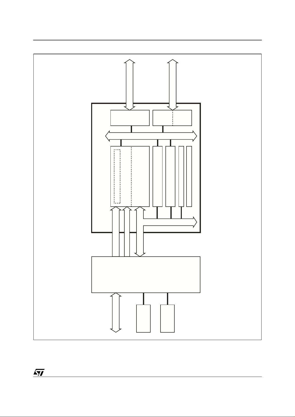
Figure 4. System Block Diagram, Two-Chip Solution
DSM2180F3
AI04910
I/O, PLD, CHIP SELECTS
8 I/O
DSM2180F3
DSP SYSTEM MEMORY
MEM PAGE CONTROL
ADDR & DECODE LOGIC
22 ADDRESS
PORTS
128k X 8
FLASH MEMORY
8 DATA
ISP, I/O, PLD, CHIP SEL
ALL
8 I/O
I/O BUS
16 MACROCELL PLD
JTAG
PORTS
I/O CONTROL
ISP TO
AREAS
POWER MANAGEMENT
CONTENT SECURITY
WR, RD, BMS, DMS, IOMS
ANALOG
DEVICES
13 FLAGS / 4 INTR
The two-chip combination of a DSP and a DSM
device is ideal for systems which have limitations
on size, EMI levels, and power consumption. DSM
memory and logic are “zero-power”, meaning they
DSP
SERIAL
ADSP-218X
DEVICE
FAMILY
SERIAL
DEVICE
automatically go to standby between memory accesses or logic input changes , producing low active and standby current consumption, which is
ideal for battery powered products.
5/63

DSM2180F3
A programmable security bit in the DSM protects
its contents from unauthorized viewing and copying. When set, the security bit will block access of
programming devices (JTAG or others) to the
DSM Flash memory and PLD configuration. The
only way to defeat the security bit is to erase the
entire DSM device, after which the device is blank
and may be used again. The DSP will always have
access to Flash memory contents through the 8-bit
data port even while the security bit is set.
Table 1. DSM2180F3 DSP Memory System Devices
Part Number
DSM2180F3-90 128K Bytes Eight 16K Byte Sectors 16 macro cells Up to 16 5V ±10% 90 ns
ISP Flash
Memory
Flash Partitioning PLD I/O Ports
V
CC
and I/O
Mem Speed
Table 2. Compatible Analog Devices DSPs
DSP Part Numbers
ADSP- 2181, 2184, 2185, 2186 5.0 5.0V
Operating Voltage, V
CC
I/O Capability
6/63

ARCHITECTURAL OVERVIEW
Major functional blocks are shown in Figure 5.
DSP Address/Data/Control Interface
These DSP signals attach directly to the DSM inputs for a glueless connection. An 8-bit data c onnection is formed and all 22 DSP address lines
can be decoded while the DSP operates in full
memory mode. DSP memory strobes;
and
IOMS are used for BDMA, dat a, & I/O access
respectively (no program memory access,
BMS, DMS,
PMS).
Flash Memory
The 1 Mbit (128K x 8) Flash memory is divided into
eight equally-sized 1 6K byte s ect ors t hat are i ndividually selectable through the Decode PLD. Each
Flash memory sector can be located at any address as defined by the user with PSDsoft Express. The flexibility of the Decode PLD and Page
Register logic allow the DSP to access Flash
memory as Byte DMA (BDMA) or as external data
overlay memory across several memory pages.
BDMA transfers are good for initial bootloading
and for loading internal overlay memory at runtime, but BDMA is not efficient writing to Flash
memory because Flash memory is unlocked, written, and status is check ed one byt e at a time, requiring an initialization of the BDMA channel for
each and every byte transfer. The DSM device al-
DSM2180F3
lows the DSP to al ternat ively access F l ash memory as data overlay m emory (using
BMS). Writing Flash memory this way is faster and
requires simpler code. Note: During a DSP data
access using the
DMS strobe, only the upper b yte
of a 16-bit DSP data word is used.
DSM Flash memory sector size of 16K bytes
matches the DSP external Data M emory Overlay
window size of 16K locations (two 8K windows
when DMOVLAY register is used, see Analog Devices ADSP-218X data sheets). This alignment
provides convenient data management. Also,
each 16K byte sector can be loaded with contents
from different firmware or data files specified in
PSDsoft Express
TM
.
Miscellaneous: The DSP can erase Flash memory
by individual sectors or the entire Flash memory
array may be erased at one time. The Flash memory automatically goes to standby between D SP
read or write accesses to conserve power. Maximum access times include sector decodi ng time.
Maximum erase cycles is 100K and data retention
is 15 years minimum. Flash memory, as well as
the entire DSM device may be program med with
the JTAG ISP interface with no DSP involvement.
DMS instead of
7/63

DSM2180F3
Figure 5. B lo ck D ia gram
SECURITY
DSP
ADDR
AD0
AD1
AD2
AD3
AD4
AD5
AD6
AD7
AD8
AD9
AD10
AD11
AD12
AD13
AD14
AD15
PC2
PC7
DSP
CONTROL
CNTL0
CNTL1
CNTL2
PD0
PD1
PD2
RST\
LOCK
INTERNAL ADDR, DATA, CONTROL BUS LINKED TO DSP
PAGE REG
fs5
fs4
DECODE PLD
EXTERNAL
CHIP SELECTS
COMPLEX PLD
PLD INPUT BUS
PIN FEEDBACK
NODE FEEDBACK
(DPLD)
(CPLD)
AND
ARRAY
FS0-7
CSIOP
EXTERNAL CHIP SELECTS, ESC0-2
3 OPTIONAL OUTPUTS TO PORT D
A
B
B
C
16 OUTPUT MICRO<>CELLS
B
C
fs3
fs2
fs1
fs0
8 SEGMENTS, 16 KB
POWER MANAGEMENT
A
A
A
B
B
B
B
B
B
C
C
C
B
B
B
C
C
C
16 INPUT
MICRO<>CELLS
128 KBytes TOTAL
RUNTIME CONTROL
CSIOP REGISTER FILE
C
B
C
FLASH MEMORY
fs7
fs6
A
A
A
A
B
B
B
B
B
B
B
B
C
C
C
B
B
B
C
C
C
ALLO-
CATOR
JTAG-ISP
TO ALL AREAS
OF CHIP
DSM2180F3
DSP SYSTEM
MEMORY
DSP
DATA
PA0
PA1
PA2
PA3
PA4
PA5
PA6
PA7
I/O PORT
PB0
PB1
PB2
PB3
PB4
PB5
PB6
PB7
I/O PORT
PC0
PC1
PC3
PC4
PC5
PC6
AI04911
Programm a b le Logic (PLDs)
The DSM family contains two PLDS that m ay optionally run in Turbo or Non-Turbo mode. PLDs operate faster (less propagation delay) while in
Turbo mode but consume more power than NonTurbo mode. Non-Turbo mode allows the PLDs to
automatically go to standby when no inputs are
change to conserve power. The Turbo mode setting is controlled at runtime by DSP software.
Decode PLD (DPLD). This is programmable logic used to select one of the eight individual Flash
memory segments or the group of control registers
within the DSM device. The DPLD can also optionally drive external chip select signals on Port D
pins. DPLD input signals include: DSP address
and control signals, Page Register outputs, DSM
Port Pins, CPLD logic feedback.
Complex PLD (CPLD). This programmable logic
is used to c reate bo th combinatorial and sequential general purpose logic. The C PLD contains 16
Output Macrocells (OMCs) and 16 Input Macrocells (IMCs). PSD macrocell registers a re unique
in that that have direct connection to the DSP data
bus allowing them to be loaded and read directly
by the DSP at runtime. This di rect access is good
for making small peripheral devices (shifters,
counters, state machines, etc.) that are accessed
directly by the DSP with little overhead. DPLD inputs include DSP address and control signals,
Page Register outputs, DSM Port Pins, and CPLD
feedback.
OMCs: The general structure of the CPLD is similar in nature to a 22V10 PLD device wit h t he familiar sum-of-products (AND-OR) construct. True
and compliment versions of 64 input signals are
available to a large AND array. AND array outputs
feed into a multiple product-term O R gate within
each OMC (up to 10 product-terms for each
OMC). Logic output of the OR gate can be passed
on as combinatorial logic or combined with a flipflop within in each OMC to realize sequential logic.
OMCs can be used a s a buried nodes with feedback to the AND array or OMC output can be routed to pins on Port B or PortC.
IMCs: Inputs from pins on Port B or Port C are
routed to IMCs for conditioning (clocking or latching) as they enter the chip, which is good for sampling and debouncing inputs. Alternatively, IMCs
can pass Port input signals directly to P LD inputs
8/63

DSM2180F3
without clocking or latching. The DSP may read
the IMCs at any time.
Runtime Control Registers
A block of 256 byt es is decoded inside the DSM
device as DSM control and status registers. 27
registers are used in the block of 256 locations to
control the output state of I/O pins, to read I/O
pins, to control p ower managem ent, to read /write
macrocells, and other functions at runtime. See
Table 4 for description. The base address of these
256 locations is referred to in this data sheet as
csiop
(Chip Select I/O Port). Individual registers
within this block are accessed with an offset from
csiop
the base address. The DSP accesses
ters using I/O memory with the
IOMS strobe.
regis-
csiop
registers are accessed as bytes, so only the lower
half of a DSP I/O word is used during access.
Memory Page Register
This 8-bit register can be l oaded and read b y the
csiop
DSP at runtime as one of the
registers. Its
outputs feed directly into the PLDs. The page register is a powerful feature that allows the DSP to
access all 128K Bytes of DSM Flash memory in
16K byte pages. This s ize matches the 16K location data overlay window the AD SP-218X family.
Page register outputs may also be used as CP LD
inputs for general use.
I/O Po r t s
The DSM has 19 individually configurable I/O pins
distributed over the three ports (Ports B, C, and D).
Each I/O pin can be individually configured for different functions such as standard MCU I/O p orts
or PLD I/O on a pin by pin basis. (MCU I/O means
that for each pin, its output state can be controlled
or its input value can be read by the DSP at runt-
csiop
ime using the
registers like an MCU would
do.)
Port C hosts the JTAG ISP signals. Sinc e JTAG-
ISP does not occur frequently during the life of a
product, those Port C pins are under-utilized. In
applications that need every I/O pin, JTAG signals
can be multiplexed with general I/O signals to use
them for I/O when not performing ISP. See section
titled “Programming In-Circuit using JTAG ISP” on
page 41 for muxing JTAG pins on Port C, and Application Note
AN1153
The static configuration of all Port pins is d efined
with the PSDsoft Express
.
TM
software development tool. The dynami c ac tion of th e P orts p ins is
controlled by DSP runtime software.
JTAG ISP Port
In-System Programming (ISP) can be pe rformed
through the JTAG signals on Port C. This serial interface allows programming of the entire DSM
device or subsections (t hat is, only Flash me mory
but not the PLDs) without the participation of the
DSP. A blank DSM device soldered to a circuit
board can be completely programmed in 10 to 20
seconds. The basic JTAG signals; TMS, TCK,
TDI, and TDO form the IEEE-1149.1 interface.
The DSM device does not implement the IEEE-
1149.1 Boundary Scan funct ions. The DSM uses
the JTAG interface for ISP only. However, the
DSM device can reside i n a st andard J TAG ch ain
with other JT AG devic es and it will r emain in BY PASS mode while other devices perform Boundary Scan.
ISP programming time can be reduced as much as
30% by using two more signals on Port C, TSTAT
and TERR
The FlashLINK
in addition to TMS, TCK, TDI and TDO.
TM
JTAG programming cable is
available from STMicroelectronics for $59USD
and PSDsoft Express software is available at no
charge from www.psdst.com. That is all that is
needed to program a DSM device using the parallel port on any PC or note-book. See section titled
“Programming In-Circuit using JTAG ISP” on page
41.
Power Management
csiop
The DSM has bits in
control registers that
are configured at run -time by the DSP to reduce
power consumption of the CPLD. The Turbo bit in
the PMMR0 register can be set to logic 1 and the
CPLD will go to Non-Turbo mode, meaning it will
latch its outputs and go to sleep until the next transition on its inputs. There is a slight penalty in PLD
performance (longer propagation delay), but significant power savings are realized.
csio p
Additionally, bits in two
registers can be set
by the DSP to selectively block signals from entering the CPLD which reduces power consumption.
See section titled “Power Management” on page
39.
Security and NVM Sector Protection
A programmable security bit in the DSM protects
its contents from unauthorized viewing and copying. When set, the security bit will block access of
programming devices (JTAG or others) to the
DSM Flash memory and PLD configuration. The
only way to defeat the security bit is to erase the
entire DSM device, after which the device is blank
and may be used again.
Additionally, the content s of ea ch in dividual F lash
memory sector can be write protected (sector protection) by configuration with PSDsoft Express
TM
This is typically used to protect DSP boot code
from being corrupted by inadvertent writes to
Flash memory from the DSP.
Pin Assign m ent s
Pin assignment are shown for the 52-pin PLCC
package in F igure 2, and the 5 2-pin PQFP package in Figure 3.
.
9/63

DSM2180F3
Table 3. Pin Description
Pin Name Type Description
ADIO0-15 In Sixteen address inputs from the DSP.
CNTL0 In Active low write strobe input (WR
CNTL1 In Active low read strobe input (RD
CNTL2 In Active low Byte Memory Select (BMS
Reset
PA0-7 I/O Eight data bus signals connected to DSP pins D8 - D15.
PB0-7 I/O
PC0-7 I/O
PD0-2 I/O
V
CC
GND Ground pins
Active low reset input from system. Resets DSM I/O Ports, Page Register contents, and other
In
DSM configuration registers. Must be logic Low at Power-up.
Eight configurable Port B signals with the following functions:
1. MCU I/O – DSP may write or read pins directly at runtime with csiop registers.
2. CPLD Output Macrocell (McellAB0-7 or McellBC0-7) outputs.
3. Inputs to the PLDs (Input Macrocells).
Note: Each of the four Port B signals PB0-PB3 may be configured at run-time as either standard
CMOS or for high slew rate. Each of the four Port B signals PB3-PB7 may be configured at
run-time as either standard CMOS or Open Drain Outputs.
Eight configurable Port C signals with the following functions:
1. MCU I/O – DSP may write or read pins directly at runtime with csiop registers.
2. CPLD Output Macrocell (McellBC0-7) output.
3. Input to the PLDs (Input Macrocells).
4. Pins PC0, PC1, PC5, and PC6 can optionally form the JTAG IEEE-1149.1 ISP serial
interface as signals TMS, TCK, TDI, and TDO respectively.
5. Pins PC3 and PC4 can optionally form the enhanced JTAG signals TSTAT and TERR
respectively. Reduces ISP programming time by up to 30% when used in addition to the
standard four JTAG signals: TDI, TDO, TMS, TCK.
6. Pin PC3 can optionally be configured as the Ready/Busy output to indicate Flash memory
programming status during parallel programming. May be polled by DSP or used as DSP
interrupt to indicate when Flash memory byte programming or erase operations are
complete.
Note 1: Port C pin PC2 input (or any PLD input pin) can be connected to DSP D18 output which
Note 2: Port C pin PC7 input (or any PLD input pin) can be connected to DSP D19 output which
Note 3: When used as general I/O, each of the eight Port C signals may be configured at run-time
Note 4: The JTAG ISP pins may be multiplexed with other I/O functions.
Three configurable Port D signals with the following functions:
Note 1: It is recommended to connect Port D pin PD0 input to DSP IOMS
Note 2: It is recommended to connect Port D pin PD1 input to DSP DMS
Note 3: It is recommended to connect Port D pin PD2 input to DSP PWDACK output if the DSP
Supply Voltage
functions as DSP address A16 in DSP Full Memory Mode. See Figure 6.
functions as DSP address A17 in DSP Full Memory Mode. See Figure 6.
as either standard CMOS or Open Drain Outputs.
1. MCU I/O – DSP may write or read pins directly at runtime with csiop registers.
2. Input to the PLDs (no associated Input Macrocells, routes directly into PLDs).
3. CPLD output (External Chip Select). Does not consume Output Macrocells.
4. Pin PD1 can optionally be configured as CLKIN, a common clock input to PLD.
5. Pin PD2 can optionally be configured as CSI
memory. Flash memory is disabled to conserve more power when CSI
connect CSI
active low I/O Memory Select strobe. See Figure 6.
low Data Memory Select strobe. See Figure 6.
Power Down mode is used. See Figure 6.
to ADSP-218X PWDACK output signal.
) from the DSP
) from the DSP.
) signal from the DSP.
, an active low Chip Select Input to select Flash
is logic high. Can
output which is the
output which is the active
10/63

TYPICAL CONNECTIONS
Figure 6 shows a typical connection scheme.
Many connection possibilities exist since most
DSM pins are multipurpose. The sc hem e i llustrated is ideal for a design that needs fast JTAG ISP,
Eight additional general I/O with PLD capability,
access to Flash mem ory as By te DM A or as Dat a
Overlay memory, and the DSP uses Power Down
mode. If your design needs more I/O, or Byte DM A
access to Flash memory is all that is needed (no
Data Overlay), or lowest power consumption is not
an issue, then consider the following options.
Port C JTAG: Figure 6 shows all six JTAG signals in use full time (not multiplexed with I/0). Using six-pin JTAG can reduce ISP time by as much
as 30% compared to four-pin JTAG. Alternatively,
four-pin JTAG (TMS, TCK, TDI, TDO) can be used
if more general I/O pins are needed and the few
extra seconds of programming time is not crucial,
freeing up pins PC3 and PC4. Other JTAG options
include mutiplexing JTAG pins with general I/O
(see “Programming In-Circuit using JTAG ISP” on
page 41 and Application Not e
ing JTAG at all. If no JTAG is used, the DSM device has to be programmed on a conventional
AN1153
) or not us-
DSM2180F3
programmer before it is installed on the circuit
board. Using no JTAG makes more I/O available.
Pin PD 1 . If Flash memory will be accessed only
using Byte DMA mode in your design, and no external Data Overlay memory accesses are used,
then pin PD1 can be used for other purposes
(MCUI/O, common CPLD clock input, external
chip select, or PLD input)
Pin PD 2 . If the DSP will not use Power Down
mode, then PD2 can be used for other purposes
(MCUI/O, external chip select, PLD input)
Pins PC2 and PC7. In Figure 6, these two pins
are used as dedicated address inputs connect ed
to DSP address outputs. This wil l route DSP address signals A16 and A17 directly into the DPLD.
Be aware that any free pin on Port B, Port C, or
Port D may be used for DSP address inputs, it
does not have to be pins PC2 and PC7.
Pin PB0. This pin is shown as a chip select for an
external peripheral device such as a 16450 or
16550 UART. Equivalent ly, any free pin on Ports
B, C, or D may be used for this.
11/63

DSM2180F3
Figure 6. Typical Connections
DEVICE
OPTIONAL
PARALLEL
(UART, ETC)
AI04912
CONNECTOR
JTAG-ISP
DATA
WRITE
DATA8..15
_WR
READ
_RD
ADDR0..2
_SELECT
ADDRESS
DSM2180F3
DATA8
VCC
I/O
I/O
I/O
I/O
I/O
I/O
I/O
CHIP SEL
PB3
PB2
PB1
PB0
PA1
PA4
PA2
D10
DATA11
D11
PA3
DATA12
D12
DATA13
D13
PA6
PA5
PA7
WRITE
DATA14
DATA15
D14
D15
PA0
DATA9
DATA10
D9
D8
PD1
CNTL1
CNTL0
CNTL2
PD0
READ
I/O MEM SELECT
BYTE MEM SELECT
DATA MEM SELECT
_RD
_WR
_BMS
_DMS
_IOMS
PB7
PB6
PB5
PB4
ADIO0
ADIO1
ADIO2
ADDR1
ADDR0
ADDR2
ADDR3
N/C
A0A1A2A3A4A5A6A7A8
_PMS
_CMS N/C
ADIO3
ADIO4
ADDR4
ADIO5
ADIO6
ADDR6
ADDR5
ADIO7
ADDR7
TMS
TCK
PC1
PC0
ADIO8
ADIO9
ADDR8
ADDR9
A9
TSTAT
PC3
ADIO10
ADDR10
A10
_TERR
TDI
TDO
PC4
PC5
ADIO11
ADIO12
ADDR13
ADDR11
ADDR12
A11
A12
GND
_RESET
PC6
ADIO13
ADIO14
ADIO15
ADDR14
ADDR15
A13
D16
D17
PC2
PC7
ADDR17
ADDR16
D18
D19
_RESET
_RESET
POWER DOWN
_RESET
PWDACK PD2/_CSI
12/63
_BR
ADSP-218X
BUS_REQUEST
BUS_GRANT
_BG
_BGH
_PWD
GRANT_HUNG
PWR_DOWN_IN
CLKIN
XTAL
XTAL
CLOCK or
I/O
FL0
I/O
FL1
I/O
FL2
PF3
PF0/MODEA
PF1/MODEB
PF2/MOCEC
I/O
I/O
I/O
I/O
INTR/I_O
_IRQL0/PF5
_IRQL1/PF6
_IRQ2/PF7
_IRQE/PF4
INTR/I_O
INTR/I_O
INTR/I_O
SPORT0
SERIAL CHN
SERIAL
DEVICE
SPORT1
SERIAL CHN
SERIAL
DEVICE
_RESET

MEMORY MAP
Figure 7 shows a typical system memory map.
The nomenclature
Flash memory segm ent desi gnators.
fs0..fs7
are individual 16K Byte
csiop
designates the DSM control register block. The DSP
runs in Full Memory Mode. Memory contents of
the DSM device may lie in one or more of t hree different DSP address spaces; I/O space, Byte DMA
space, and/or External Data Overlay Memory
space. Since the DSM device is a byte-wide memory, it typically is not used in DSP Program Memory space (
PMS active).
The designer may easily specify memory mapping
in a point-and-click software environment using
PSD so ft E x pr es s
TM
. Since the memory mapping is
implemented with the DPLD and the Page Register, many possibilities exist. Figure 7 shows a typical memory map with the following attributes:
I/O Address Space. The 256 byte locations for
csiop
DSM control registers (
address space, selected by the DSP
) reside in DSP I/O
IOMS signal.
Since DSP I/O accesses are by 16 bits, not 8 bits,
the upper byte of a 16-bit DSP I/O access must be
ignored.
Byte DMA Address Space. The DSP m ay bootload or fetch overlay bytes from 128K Bytes of
Flash memory using the DSP BDMA channel. The
DSP may also write to Flash memory using the
Byte DMA channel. DSM Flash memory is accessed in 128K continuous byte address locations
DSM2180F3
through the BDMA channel and is selected whenever the DSP
Flash memory in the DSM device must be unlocked and written by the DSP one byte at a time,
checking status after each write (typical Flash
memory programming algorithm). A DMA channel
is not optimum for this scenario since the c han nel
must be initialized on each byte access. That is
why the 128K Bytes of F lash memory also lie in
DSP Data Overlay Memory space as described
next.
Data Overlay Memory Address Space. All
128K Bytes of Flash mem ory also reside in DSP
External Data Overlay Memory space, selected by
DMS, allowing more efficient byte writes to Flash
memory. The DSP uses its external data overlay
window of 8K locations to access external memory
as data. The DSP doubles the size of this window
to 16K locations by manipu lating its A13 address
line using its DMOVLAY register (See ADSP-218X
data sheets for details). Since all 128K Bytes of
Flash memory must be accessed through a window of only 16K locations, the DSP uses the Page
Register inside the DSM device to page through 8
pages of 16K Bytes as shown in Figure 7. Since
DSP Data accesses are by 16 bits, not 8 bi ts, t he
upper byte of a 16-bit DS P Data access m ust be
ignored.
BMS signal is active.
13/63
DSM2180F3
Figure 7. Typ ic a l Sy st em Mem ory Map
)
DMS
1FFFF
03FFF
A13 = 1
00000
A13 = 0
fs7
PAGE 7
A13 = 1
A13 = 0
fs6
PAGE 6
A13 = 1
A13 = 0
fs5
PAGE 5
A13 = 1
A13 = 0
fs4
PAGE 4
A13 = 1
A13 = 0
fs3
PAGE 3
A13 = 1
fs2
Flash Memory Paged Over 8 Pages
PAGE 2
PAGE 1
A13 = 0
A13 = 1
fs1
A13 = 1
AI04913
A13 = 0
A13 = 0
Space (
DSP Data Memory
)
BMS
fs7
16 KBytes
1FFFF
Flash Memory
1C000
1BFFF
Space (
DSP Byte DMA Memory
)
IOMS
Space (
DSP I/O Memory
1FFFF
fs6
16 KBytes
Flash Memory
18000
17FFF
fs5
16 KBytes
Flash Memory
14000
13FFF
fs4
16 KBytes
Nothing
Mapped
Flash Memory
10000
0FFFF
Nothing
Mapped
fs3
16 KBytes
Flash Memory
0C000
0BFFF
fs2
16 KBytes
Flash Memory
08000
07FFF
fs1
16 KBytes
PAGE 0
03FFF
Flash Memory
04000
03FFF
_cs_uart
8 UART REGS
00200
00208
fs0
16 KBytes
(8 KWords)
00000
fs0
16 KBytes
Flash Memory
00000
csiop
256 CONTROL REGS
00000
000FF
14/63

DSM2180F3
SPECIFYI N G MEM MAP WI TH PSD SO FT EXPRESS
The memory map shown in Figure 7 can be easily
specified with PSDsoft Express
click environment. PSDsoft Ex press
TM
in a point-and-
TM
will gener-
TM
ments of the ABEL language. Figure 8 shows the
resulting equations generated by PSDsoft ExpressTM.
ate Hardware Definition Language (HDL) state-
Figure 8. HDL Statements Generated from PSDsoft Express to Implement Memory M ap
csiop = ((address >= ^h0000) & (address <= ^h00FF) & (!_ioms & _dms & _bms));
fs0 = ((address >= ^h0000) & (address <= ^h3FFF) & (_ioms & _dms & !_bms))
# ((page == 0) & (address >= ^h0000) & (address <= ^h3FFF) & (_ioms & !_dms &
fs1 = ((address >= ^h4000) & (address <= ^h7FFF) & (_ioms & _dms & !_bms))
# ((page == 1) & (address >= ^h0000) & (address <= ^h3FFF) & (_ioms & !_dms &
fs2 = ((address >= ^h8000) & (address <= ^hBFFF) & (_ioms & _dms & !_bms))
# ((page == 2) & (address >= ^h0000) & (address <= ^h3FFF) & (_ioms & !_dms &
fs3 = ((address >= ^hC000) & (address <= ^hFFFF) & (_ioms & _dms & !_bms))
# ((page == 3) & (address >= ^h0000) & (address <= ^h3FFF) & (_ioms & !_dms &
fs4 = ((address >= ^h10000) & (address <= ^h13FFF) & (_ioms & _dms & !_bms))
# ((page == 4) & (address >= ^h0000) & (address <= ^h3FFF) & (_ioms & !_dms &
fs5 = ((address >= ^h14000) & (address <= ^h17FFF) & (_ioms & _dms & !_bms))
# ((page == 5) & (address >= ^h0000) & (address <= ^h3FFF) & (_ioms & !_dms &
fs6 = ((address >= ^h18000) & (address <= ^h1BFFF) & (_ioms & _dms & !_bms))
# ((page == 6) & (address >= ^h0000) & (address <= ^h3FFF) & (_ioms & !_dms &
fs7 = ((address >= ^h1C000) & (address <= ^h1FFFF) & (_ioms & _dms & !_bms))
# ((page == 7) & (address >= ^h0000) & (address <= ^h3FFF) & (_ioms & !_dms &
! _cs_uart = ((address >= ^h0200) & (address <= ^h0207) & (!_ioms & _dms & _bms));
_bms));
_bms));
_bms));
_bms));
_bms));
_bms));
_bms));
_bms));
Specifying these equations using PSDsoft Ex-
TM
press
is very simple. Figure 9 shows how to
specify the equation for the 16K Byt e Fl ash memory segment,
. Notice how
fs2
can reside in two
fs2
different address spaces depending on the state of
the control signals from the DSP (
IOMS, DMS, or
BMS) and the memory page number coming from
the DSM Page Register outputs. This specification
process is repeated for all other Flash memory
csiop
segments, the
register block, and any exter-
nal chip select signals (UART , etc.).
15/63

DSM2180F3
Figure 9. PSDsoft ExpressTM Memory Mapping
AI03779
16/63

RUNTIME CONTROL REGISTER DEFINITION
There are up to 256 addresses decoded inside the
DSM device for control and status information. 27
of these locations contain registers that the DSP
can access at runtime. The base address of this
block of 256 locations is referred to in this manual
as
csiop
(Chip Select I/O Port). Table 4 lists the 27
registers and their offsets (in hex) from the
csiop
base address needed to access individual DSM
control and status registers. Th e DSP will a ccess
these registers in I/O memory space using its
IOMS
DSM2180F3
strobe. These registers are accesses in bytes, so
the DSP should ignore the u pper by te of its 16-bit
I/O access.
Note1: All
reset.
Note2: Do not write to unused locations within the
csiop
logic zero.
csiop
registers are cleared to logic 0 at
block of 256 registers. They should remain
Table 4.
Data In 01 10 11
Data Out 05 12 13
Direction 07 14 15
Drive Select 09 16 17
Input Macrocells 0B 18 Read to obtain state of IMCs. No writes.
Enable Out 0D 1A 1B
Output Macrocells AB 20
Output Macrocells BC 21
Mask Macrocells AB 22
Mask Macrocells BC 23
CSIOP
Register Name Port B Port C P ort D Other Description
Registers and their Offsets (in hex)
MCUI/O input mode. Read to obtain current logic level of
Port pins. No writes.
MCU I/O output mode. Write to set logic level on Port
pins. Read to check status.
MCU I/O mode. Configures Port pin as input or output.
Write to set direction of Port pins.
Logic 1 = out, Logic 0 = in. Read to check status.
Write to configure Port pins as either standard CMOS or
Open Drain on some pins, while selecting high slew rate
on other pins. Read to check status.
Read to obtain the status of the output enable logic on
each I/O Port driver. No writes.
Read to get logic state of output of OMC bank AB.
Write to load registers of OMC bank AB.
Read to get logic state of output of OMC bank BC.
Write to load registers of OMC bank BC.
Write to set mask for loading OMCs in bank AB. A logic
1 in a bit position will block reads/writes of the
corresponding OMC. A logic 0 will pass OMC value.
Read to check status.
Write to set mask for loading OMCs in bank BC. A logic
1 in a bit position will block reads/writes of the
corresponding OMC. A logic 0 will pass OMC value.
Read to check status.
Flash Sector Protect C0
Security Bit C2
JTAG Enable C7
PMMR0 B0 Power Management Register 0. Write and read.
PMMR2 B4 Power Management Register 2. Write and read.
Page E0 Memory Page Register. Write and read.
Read to determine Flash Sector Protection Setting. No
writes.
Read to determine if DSM devices Security Bit is active.
Logic 1 = device secured. No writes.
Write to enable JTAG Pins (optional feature). Read to
check status.
17/63

DSM2180F3
DETAILED OPERATION
Figure 5 shows major functional areas of the device :
■ Flash Memory
■ PLDs (DPLD, CPLD, Page Register)
■ DSP Bus Interface (Address, Data, Control)
■ I/O Por ts
■ Runtime Control Registers
■ JTAG ISP Interface
The following describes these functions in more
detail.
Flash Memory
The Flash memory array is divided evenly into
eight equal 16K byt e sectors. Each sector is selected by the DPLD can be separately protected
from program and erase cycles. This configuration
is specified by using PSDsoft Express
Memory Sector Select Signals. The DPLD generates the Select signals for all the internal memory blocks (see Figure 14). Each of the eight sectors
of the Flash memory has a Select signal (
FS7
) which contains up to three product terms.
Having three product terms for each Selec t signal
allows a given sector to be mapped into multiple
areas of system memory.
Ready/Busy
output the Ready/
output on Ready/
(PC3 ). This signal can be used to
Busy status of the device. The
Busy (PC3) is a 0 (Busy) when
Flash memory is being written,
memory is being erased. The output is a 1 (Ready)
when no Write or Erase cycle is in progress. This
signal may be polled by the DSP or used as a DSP
interrupt to indicate when an erase or program cycle is complete.
TM
.
or
when Flash
FS0-
Memory Operation. The Flash memory is accessed through the DSP Address, Data, and Control Bus Interface. The DSP can access Flash
memory as BDMA mode or as External Data
Memory Overlay. But from the DSM perspective, it
sees either type of access as a series of byte operations (reads and writes). If the DSP accesses
the DSM in BDMA mode, then the DSP BDMA
channel must be initia lized and run for eac h byte
(or block of bytes) read from Flash memory or it
must initialize the DMA channel for each byte written to Flash mem ory. Alternat ively, if t he DS P ac cesses the DSM in External Data Memory Overlay
mode, then the DSP mu st only ensure the PSD
Page Register and the DSP DMOVLAY register
contains the correct va lue, then it performs a normal data read or data write operat ion without the
burden of initializing the BDMA channel for each
operation (upper byte of 16-bit word is ignored).
DSPs and MCUs cannot write to Flash memory as
it would an SRAM device. Flash memory must first
be “unlocked” with a special sequence of byte
write operations to invoke an internal algorithm,
then a single data byte is written to the Flash memory array, then programming status is chec ked by
a byte read operation or by checking the Ready/
Busy
pin (PC3). Table 5 lists all of the special instruction sequences to program (write) data to the
Flash memory a rray, erase the array, and check
for different types of s tatus from t he array. T hese
instruction sequences are different combinations
of individual byte write and byte read operations.
Once the Flash memory array is programmed
(written) and then it is in “Read Array” mode, the
DSP will read from Flash memory just as if would
from any 8-bit ROM or SRAM device.
18/63

DSM2180F3
Table 5. Instruction Sequences
Instruction
Sequence
Cycle 1 Cycle 2 Cycle 3 Cycle 4 Cycle 5 Cycle 6 Cycle 7
1,2,3,4
Read byte
Read Memory
Contents
5
from any
valid Flash
memory addr
Read identifier
Read Flash
Identifier
6,7
Write AAh to
XX555h
Write 55h
to XXAAAh
Write 90h
to XX555h
with addr lines
A6,A1,A0 =
0,0,1
Read Memory
Sector Protection
6,7,8
Status
Program a Flash
Byte
Flash Bulk Erase
Flash Sector
10
Erase
Write AAh to
XX555h
Write AAh to
XX555h
Write AAh to
9
XX555h
Write AAh to
XX555h
Write 55h
to XXAAAh
Write 55h
to XXAAAh
Write 55h
to XXAAAh
Write 55h
to XXAAAh
Write 90h
to XX555h
Write A0h
to XX555h
Write 80h
to XX555h
Write 80h
to XX555h
Read identifier
with addr lines
A6,A1,A0 =
0,1,0
Write
(program)
data to addr
Write AAh to
XX555h
Write AAh to
XX555h
Write 55h
to XXAAAh
Write 55h
to XXAAAh
Write 10h
to XX555h
Write 30h
to another
Sector
Write 30h
to another
Sector
Write B0h to
Suspend Sector
11
Erase
address that
activates any
of FS0 - FS7
Write 30h to
Resume Sector
12
Erase
addr that
activates any
of FS0 - FS7
Write F0h to
Reset Flash
6
address that
activates any
of FS0 - FS7
Note: 1. All v al ues are in hexad ecimal, X = Don’t Care
2. A desired internal Flash memory sector select signal (FS0 - FS7) must be active for each write or read cycle. Only one of FS0 - FS7
will be active at any given time depending on the address presented by the DSP and the memory mapping defined in PSDsoft Expres s . F S 0 - F S 7 are active high logic in ternally.
3. DS P addres ses A17 through A 12 are Don’t Care duri ng the inst ruction s equence de coding . Only addre ss bit s A11-A0 are used
during Flash memory instruction sequence decoding bus cycles. The individual sector select signal (FS0 - FS7) which is active during the instruction sequ ences determi nes the comple te address.
4. For write operations, addresses are latched on the falling edge of Write Strobe (WR
Write Strobe (WR
5. No Unlock or Inst ruction cycles are required when the dev i ce is in the Read A rray mode. Operation is like reading a ROM de vice.
6. The Reset Flash instruction is required to return to the normal Read Array mode if the Error Flag (DQ5) bit goes High, or after reading the Flash I dentifier or af t er reading the Sector Prote ct i on Status.
7. The DSP cannot invoke this instruction sequence while executing code from the same Flash memory as that for which the instruction sequence is intended. The DSP must fetch, for example, the code from the DSP SRAM when reading the Flash memory Identifier or Sector Protection Status.
8. T he data is 00h f or an unprote cted sector, and 01h for a pr otected s ector. In the fo urth cycle, the Sector Sel ect is acti ve, and
(A1,A0)= (1,0)
9. Directing this comma nd to any in dividua l active Flash memory seg ment (FS 0 - FS7) will invoke th e bulk era se of all eight Flash
memory sectors.
10. DSP writes command sequece to initial segment to be erased, then writes the byte 30h to additional sectors to be erased. The byte
30h must be ad dressed to one of the ot her Flas h memory s egment s (FS0 - FS 7) for each addition al segme nt (write 30h to any
address within a desired sector). No more than 80uS can elapse between subseq uent additiona l sector erase commands.
11. The system m ay per form R ead and P ro gram cyc les i n non- era sin g sec tors , rea d the Flas h ID o r r ead t he Se ctor Prot ect Sta tus,
when in the Suspend Sector Erase mode. The Suspend Sector Erase instruction sequence is valid only during a Sector Erase cycle.
12. The Resume Sector Erase instruction sequence is valid only during the Suspend Sector Erase mode.
, CNTL0)
, CNTL0), Dat a i s latched on the rising edge of
19/63

DSM2180F3
Instruction Sequences
An instruction sequence consists of a sequence of
specific write or read operations. Each byte written
to the device is received and sequentially decoded
and not executed as a standard write operation to
the memory array. The instruction sequence is executed when the correct number of bytes are properly received and the time between two
consecutive bytes is shorter than the time-out period. Some instruction sequences are structured to
include read operations after the initial write operations.
The instruction sequence must be followed exac tly. Any in valid com binatio n of ins truction bytes o r
time-out between two consecutive bytes while addressing Flash memory resets the device logic into
Read Array mode (Flash memory is read like a
ROM device). The device s upports the instruction
sequences summarized in Table 5:
Flash memory:
■ Erase memory by chip or sector
■ Suspend or resume sector erase
■ Program a Byte
■ Reset to Read Array mode
■ Read primary Flash Identifier value
■ Read Sector Protection Status
These instruction sequences are detailed in Table
5. For efficient decoding of the instruction sequences, the first two bytes of an i nstruction sequence are the coded cycles and are followed by
an instruction byte or confirmation byte. The coded
cycles consist of writing the data AAh to address
XX555h during the first cycle and data 55h to address XXAAAh during the second cycle. Address
signals A17-A12 are Don’t Care during the instruction sequence Write cycles. However, the appropriate internal Sector Select (
FS0-FS7
) must be
selected internally (active, which is logic 1).
Reading Flash Memory
Under typical conditions, the D SP may read the
Flash memory using read operations just as it
would a ROM or RAM device. Alternately, the DSP
may use read operations to obtain status information about a Program or Erase cycle that is currently in progress. Lastly, the DSP may use
instruction sequences to read special data from
these memory blocks. The following sections describe these read instruction sequences.
Read Memory Contents. Flash memory is
placed in the Read Array mode after Power-up,
chip reset, or a Reset Flash memory instruction
sequence (see Table 5). The DSP can read the
memory contents of the Flash memory by using
read operations any time the read operation is not
part of an instruction sequence.
Read Flash Identifier. The Flash mem ory identifier is read with an instruction sequence composed
of 4 operations: 3 spec ific write operations and a
read operation (see T able 5). Duri ng t he read operation, address bits A6, A1, and A0 must be
0,0,1, respectively, and the appropriate internal
Sector Select (
FS0-FS7
) must be active. The iden-
tifier 0xE3.
Read Memory Sector Protection Status. The
Flash memory Sector Protection Status is read
with an instruction sequence composed of 4 operations: 3 specific write operations and a read operation (see Table 5). During the read operation,
address bits A6, A1, and A0 must be 0,1,0, respectively, while internal Sector Select (FS0-FS7)
designates the Flas h memory sector whose protection has to be verified. The read operation produces 01h if the Flash memory sector is protected,
or 00h if the sector is not protected.
The sector protection status can also be read by
the DSP accessing the Flash memory Prot ection
csiop
register in
space. See the section entitled
“Flash Memory Sector Protect” for register definitions .
Table 6. Status Bit Definition
Functional Block FS0-FS7 DQ7 DQ6 DQ5 DQ4 DQ3 DQ2 DQ1 DQ0
Flash Memory
Note: 1. X = Not guar anteed value , c an be read either 1 or 0.
2. DQ7-DQ0 represent the Data Bus bits, D7-D0.
Active (the desired
segment is selected)
Data
Polling
Toggle
Flag
Error
Flag
Erase
X
Time-
out
XXX
these tasks and are defined in Table 6. The status
Reading the Erase/Program Status Bits. The
device provides several status bits to be used by
the DSP to confirm the completion of an Erase or
Program cycle of Flash memory. These st atus bits
minimize the time that the DSP spends performing
20/63
bits can be read as many times as needed.
For Flash memory, the DS P can perform a read
operation to obtain these status bits while an
Erase or Program instruction sequence is being
executed by the embedded algorithm. See the

DSM2180F3
section entitled “Programming Flash Memory”, on
page 21, for details.
Data Polling Flag (DQ7). When erasing or programming in Flash memory, the Data Polling Flag
(DQ7) bit outputs the co mplem ent of the bit bei ng
entered for programming/writing on the Data P olling Flag (DQ7) bit. Once the Program instruction
sequence or the write operation is c ompleted, t he
true logic value is read on the Data Polling Flag
(DQ7) bit (in a read operation).
Flash memory instruction features:
■ Data Polling is effective after the fourth Write
pulse (for a Program instruction sequence) or
after the sixth Write pulse (for an Erase
instruction sequence). It must be performed at
the address being programmed or at an address
within the Flash memory sector being erased.
■ During an Erase cycle, the Data Polling Flag
(DQ7) bit outputs a 0. After completion of the
cycle, the Data Polling Flag (DQ7) bit outputs
the last bit programmed (it is a 1 after erasing).
■ If the byte to be programmed is in a protected
Flash memory sector, the instruction sequence
is ignored.
■ If all the Flash memory sectors to be erased are
protected, the Data Polling Flag (DQ7) bit is
reset to 0 for about 100 µs, and then returns to
the previous addressed byte. No erasure is
performed.
Toggle Flag ( DQ6 ). The device offers another
way for determining when t he F lash memory Program cycle is completed. During the in ternal write
operation and when the Sector Select FS0-FS7 is
true, the Toggle Flag (DQ6) bit toggles from 0 to 1
and 1 to 0 on subsequent attempts to read any
byte of the memory.
When the internal cycle is complete, the toggling
stops and the data read on the Data Bus D0-7 is
the addressed mem ory byte. The device is now
accessible for a new read or write operation. The
cycle is finished when two successive reads yield
the same output data. Flash m emo ry spe cific features:
■ The Toggle Flag (DQ6) bit is effective after the
fourth write operation (for a Program instruction
sequence) or after the sixth write operation (for
an Erase instruction sequence).
■ If the byte to be programmed belongs to a
protected Flash memory sector, the instruction
sequence is ignored.
■ If all the Flash memory sectors selected for
erasure are protected, the Toggle Flag (DQ6) bit
toggles to 0 for about 100 µs and then returns to
the previous addressed byte.
Error Flag (DQ5). During a normal Program or
Erase cycle, the Error Flag (DQ5) bit is to 0. T his
bit is set to 1 when there is a failure during Flash
memory Byte Program, Sector Erase, or Bulk
Erase cycle.
In the case of Flash memory programming, the Error Flag (DQ5) bit indicates the attempt to program
a Flash memory bit from the programmed state, 0,
to the erased state, 1, whi ch is not vali d. The Error
Flag (DQ5) bit may also indicate a Time-out condition while attempting to program a byte.
In case of an error in a Flash memory Sector Erase
or Byte Progra m cycle, the Fl ash memory sector i n
which the error occurred or to which the programmed byte belongs must no longer be used.
Other Flash memory sectors may still be used.
The Error Flag (DQ5) bit is reset after a Reset
Flash instruction sequence.
Erase Time-out Flag (DQ3). The Erase Timeout Flag (DQ3) bit reflects the time-out period allowed between two consecutive Sec tor Erase instruction sequence bytes. The Erase Time-out
Flag (DQ3) bit is reset to 0 after a Sector Erase cycle for a time period of 100 µs + 20% unless an additional Sector Erase instruction sequence is
decoded. After this time period, or when the additional Sector Erase instruction sequence is decoded, the Erase Time-out Flag (DQ3) bit is set to 1.
Programming Flash Memory
When a byte of Flash memory is programmed, individual bits a re p ro grammed to logic 0 . You cannot program a bit in Flash memory to a logic 1
once it has b een programmed to a logic 0. A bit
must be erased to logic 1, and programmed to logic 0. That means Flash memory must be erased
prior to being programmed. A b yte o f Flash memory is erased to all 1s (FFh). The DSP may erase
the entire Flash memory array all at once or individual sector-by-sector, but not byte-by-byte.
However, the DSP may program Flash memory
byte-by-byte.
The Flash memory requires the DSP to send an instruction sequence to program a byte or to erase
sectors (see Table 5).
Once the DSP issues a Flash memory Program or
Erase instruction sequence, it must check for the
status bits for completion. The embedded algorithms that are invoked inside the device provide
several ways give status to the DSP. Status may
be checked using any of three methods: Data Polling, Data Toggle, or Ready/Busy
(pin PC3).
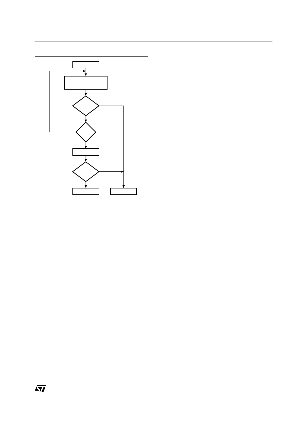
Data Polling. Polling on the Data Polling Flag
(DQ7) bit is a method of checking whether a Pro-
21/63

DSM2180F3
gram or Erase cycle is in progress or has completed. Figure 10 shows the Data Polling algorithm.
When the DSP issues a Program instruction sequence, the embedded algorithm within the device
begins. The DSP then reads the location of the
byte to be programmed in Flash memory to check
status. The Data Polling Flag (DQ7) bit of this location becomes the compliment of bit 7 of the original data byte to be programmed. The DSP
continues to poll this location, comparing the Data
Polling Flag (DQ7) bit and monitoring the Error
Flag (DQ5) bit. When the Data Polling Flag (DQ7)
bit matches bit7 of the original data, and the Error
Flag (DQ5) bit remains 0, then the em bedded algorithm is complete. If the Error Flag (DQ5) bit is
1, the DSP should test the Data Polling Flag (DQ7)
bit again since the Data Polling Flag (DQ7) bit may
have changed simultaneously wi th the Error Flag
(DQ5) bit (see Figure 10).
The Error Flag (DQ5) bit is set if either an internal
time-out occurred while the embedded algorithm
attempted to program the byte or if the DS P attempted to program a 1 to a bit that was not erased
(not erased is logic 0).
It is suggested (as with all Flash memories) to read
the location again after the embedded programming algorithm has completed, to compare the
byte that was written to the Flash memory with the
byte that was intended to be written.
When using the Data Polling method during an
Erase cycle, Figure 10 still applies. However, the
Data Polling Flag (DQ7) bit is 0 until the Erase cycle is complete. A 1 on the Error Flag (DQ5) bit indicates a time-out condition on the Erase cycle, a
0 indicates no error. The DSP can read any location within the sector being erased to get the Data
Polling Flag (DQ7) bit and the Error Flag (DQ5) bit.
PSDsoft Express generates ANSI C code functions which implement these Data Polling algorithms.
Figure 10. Data Polling Flowchart
START
READ DQ5 & DQ7
at VALID ADDRESS
DQ7
DATA
NO
DQ5
READ DQ7
DQ7
DATA
FAIL PASS
= 1
YES
=
NO
YES
YES
=
NO
AI01369B
Data Toggle. Checking the Toggle Flag (DQ6) bit
is a method o f det erm ining whether a Program or
Erase cycle is in progress or has completed. Figure 11 shows the Data Toggle algorithm.
When the DSP issues a Program instruction sequence, the embedded algorithm within the device
begins. The DSP then reads the location of the
byte to be programmed in Flash memory to check
status. The Toggle Flag (DQ6) bit of this location
toggles each time the DSP reads this location until
the embedded algorithm is complete. The DSP
continues to read this location, check ing the Toggle Flag (DQ6) bit and monitoring the Error Flag
(DQ5) bit. When the Toggle Flag (DQ6) bit stops
toggling (two consecutive reads yield the same
value), and the Error Flag (DQ5) bit remains 0,
then the embedde d algorithm is complete. If the
Error Flag (DQ5) bit is 1, the DSP should test the
Toggle Flag (DQ6) bit again, since the Toggle Flag
(DQ6) bit may have chan ged simultaneo usly with
the Error Flag (DQ5) bit (see Figure 11).
22/63
DSM2180F3
Figure 11. Data Toggle Flowchart
START
READ
DQ5 & DQ6
DQ6
=
TOGGLE
NO
DQ5
= 1
READ DQ6
DQ6
=
TOGGLE
FAIL PASS
NO
YES
YES
NO
YES
AI01370B
The Error Flag (DQ5) bit is set if either an internal
time-out occurred while the embedded algorithm
attempted to program the byte, or if the DSP attempted to program a 1 to a bit that was not erased
(not erased is logic 0).
It is suggested (as with all Flash memories) to read
the location again after the embedded programming algorithm has completed, to compare the
byte that was written to Flash memory with the
byte that was intended to be written.
When using the Data Toggle method after an
Erase cycle, Figure 11 still applies. the Toggle
Flag (DQ6) bit toggles until the Erase cycle is complete. A 1 on the Error Flag (DQ5) bit indicates a
time-out condition on the Erase cycle, a 0 indicates no error. The DSP can read any location
within the sector being erased t o get the Toggle
Flag (DQ6) bit and the Error Flag (DQ5) bit.
PSDsoft Express generates ANSI C code functions which implement these Data T oggling algorithms.
Erasing Flash Memory
Flash Bulk Erase. The Flash Bulk Erase instruc-
tion sequence uses six write operations followed
by a read o peration of the status regist er, as described in Table 5. If any byte of the Bulk Erase instruction sequence is wrong, the Bulk Erase
instruction sequence aborts and the device is re-
set to the Read Flash memory status. The Bulk
Erase command may be addresses to any one individual valid Flash memory segment (
FS0-FS7
and the entire array (all segments) will be erased.
During a Bulk Erase, the memory status may be
checked by reading the Error Flag (DQ5) bit, the
Toggle Flag (DQ6) bi t, and the Dat a Polling Flag
(DQ7) bit, as detailed in the section entitled “P rogramming Flash Memory”, on page 21. The Error
Flag (DQ5) bit returns a 1 if there has been an
Erase Failure (maximum number of Erase cycles
have been executed).
It is not necessary to program the memory with
00h because the device automatically does this
before erasing to 0FFh.
During execution of the Bulk Erase instruction sequence, the Flash memory does not accept any instruction sequences.
The address provided with the Flash Bulk Er ase
command sequence (Table 5) may select any one
of the eight internal Flash memory Sector Select
signals (FS0 - FS7). An erase of the entire Flash
memory array will occur even though the command was sent to just one Flash memory sector.
Flash Sector Erase. The Sector Erase instruction sequence uses six write operations, as described in Table 5. Additional Flash Sector Erase
codes and Flash memory sector addresses can be
written subsequently to erase other Flash memory
sectors in parallel, without further coded cycles, if
the additional bytes are transmitted in a shorter
time than the time-out period of about 100 µs. The
input of a new Sector Erase code restarts the timeout period.
The status of the internal timer can be monitored
through the level of the Erase Time-out Flag (DQ3)
bit. If the Erase Time-out Flag (DQ3) bit is 0, the
Sector Erase instruction sequence has been received and the time-out p eriod is counting. If the
Erase Time-out Flag (DQ3) bit is 1, the time-out
period has expired and the device is busy erasing
the Flash memory sector(s). Before and during
Erase time-out, any instruction sequence other
than Suspend Sector Erase an d Resume Sector
Erase instruction sequences abort the cycle that is
currently in progress, and reset the device to Read
Array mode. It is not necessary to program the
Flash memory sector with 00h as the device does
this automatically before erasing (byte=FFh).
During a Sector Erase, the memory status may be
checked by reading the Error Flag (DQ5) bit, the
Toggle Flag (DQ6) bi t, and the Dat a Polling Flag
(DQ7) bit, as detailed in the section entitled “P rogramming Flash Memory”, on page 21.
During execution of the Erase cycle, the Flash
memory accepts only Reset and Suspend Sector
Erase instruction sequences. Erasure of one
)
23/63

DSM2180F3
Flash memory sector may be suspended, in order
to read data from anot her Flash memory sector,
and then resumed.
The address provided with the initial Flash Se ctor
Erase command sequence (Table 5) must select
the first desired sector (FS0 - FS7) to erase. Subsequent sector erase commands that are appended on within the time-out period must be
addressed to other desired segments (FS0 - FS7).
Suspend Sector Erase. When a Sector Erase
cycle is in progress, the Suspend Sector Erase instruction sequence can be used to suspend the
cycle by writing 0B0h to any address when an appropriate Sector Select (FS0-FS7) is selected
(See Table 5). This allows reading of data from another Flash memory sector after the Erase cycle
has been suspended. Suspend Sector Erase is
accepted only during an Erase cycle and defaults
to Read mode. A Suspend Sector Erase instruction sequence executed during an E rase time-out
period, in addition to suspending the Erase cycle,
terminates the time out period.
The Toggle Flag (DQ6) bit stops toggling when the
device internal logic is suspended. The status of
this bit must be m onitored at an address within the
Flash memory sector being erased. The Toggle
Flag (DQ6) bit stops toggling between 0.1 µs and
15 µs after the Susp end Sector Erase instruction
sequence has been execut ed. The device i s then
automatically set to Read mode.
If an Suspend Sector Erase instruction sequence
was executed, the following rules apply:
– Attempting to read from a Flash memory sector
that was being erased outputs invalid data.
– Reading from a Flash memory sect or that was
not
being erased is valid.
cannot
– The Flash memory
be programmed, and
only responds to Resume Sector Erase and Reset Flash instruction sequences (Read is an operation and is allowed).
– If a Reset Flash instruction sequence is re-
ceived, data in the Flash memory sector that
was being erased is invalid.
Resume Sector Erase. If a Suspend Sector
Erase instruction sequence was previously executed, the erase cycle may be resumed with this
instruction sequence. The Resume Sector Erase
instruction sequence consists of writing 030h to
any address while an appropriate Sector Select
(FS0-FS7) is active. (See Table 5.)
Flash Memory Sector Protect.
Each Flash memory sector can be separately protected against Program and Erase cycles. Sector
Protection provides additional data security because it di sables all Pr ogram o r Erase cycles. This
mode can be activated through the JTAG Port or a
Device Programmer. Sector protection can be selected for each sector using PSDsoft Express.
This automatically protects selected sectors when
the device is programmed through the JTAG Port
or a Device Programmer. Flash memory sectors
can be unprotected to allow updating of their contents using the JTAG Port or a Device Programmer. The DSP can read (but cannot change) the
sector protection bits.
Any attempt to program or erase a protected Flash
memory sector is ignored by the device. The Verify
operation results in a read of the protected data.
This allows a guarantee of the retention of the Protection status.
The sector protection status can be read by the
DSP through the F lash memory protection regis-
csiop
ters (in the
block) as defined in Table 7.
Table 7. Sector Protection/Security Bit Definition – Flash Protection Register
Bit 7 Bit 6 Bit 5 Bit 4 Bit 3 Bit 2 Bit 1 Bit 0
Sec7_Prot Sec6_Prot Sec5_Prot Sec4_Prot Sec3_Prot Sec2_Prot Sec1_Prot Sec0_Prot
Note: 1. Bit Definitions:
Sec<i>_Prot 1 = Flash memory sector <i> is write protected.
Sec<i>_Prot 0 = Flash memory sector <i> is not write protected.
Table 8. Security Bit Definition
Bit 7 Bit 6 Bit 5 Bit 4 Bit 3 Bit 2 Bit 1 Bit 0
Security_Bit not used not used not used not used not used not used not used
Note: 1. Bit Definitions:
24/63
1 = Security Bi t in device has be en set.

DSM2180F3
DSM Security Bit
A programmable security bit in the DSM protects
its contents from unauthorized viewing and copying. When set, the security bit will block access of
programming devices (JTAG or others) to the
DSM Flash memory and PLD configuration. The
only way to defeat the security bit is to erase the
entire DSM device, after which the device is blank
and may be used again. The DSP will always have
access to Flash memory contents through the 8-bit
data port even while the security bit is set. The
DSP can read the status of the security bit (but it
cannot change it) by rea ding the Device Se curity
register in the
csiop
block as defined in Table 8.
Reset Flash
The Reset Flash instruction sequence resets the
internal memory logic state machine and puts
Flash memory into Read Array mode. It consists of
one write cycle (see Table 5). It must be executed
after:
– Reading the Flash Protection Status or Flash ID
– An Error condition has occurred (and the device
has set the Error Flag (DQ5) bit to 1) during a
Flash memory Program or Erase cycle.
The Reset Flash instruction sequence puts the
Flash memory back into normal Read Array mode.
It may take the Flash memory up to a few milliseconds to complete the Reset cycle. The Reset
Flash instruction sequence is ignored when it is issued during a Program or Bulk Erase cycle of the
Flash memory. The Reset Flash instruction sequence aborts any on-going Sector Erase cycle,
and returns the Flash memory to the normal Read
Array mode within a few milliseconds.
Page Re gi st er
The 8-bit Page Register increases the addressing
capability of the DSP by a factor of up to 256. The
contents of the register can also be read by the
DSP. The outputs of the Page Register (PG0PG7) are inputs to the DPLD decoder and can be
included in the Sector Select (
FS0-FS7
) equa-
tions. See Figure 12.
If memory paging is not needed, or if not all 8 page
register bits are needed for memory paging, then
these bits may be used in the CPLD for gen eral
logic. The eight flip-flops in the reg ister are connected to the internal data bus D0-D7. The DSP
can write to or read from the Page Register. The
Page Register can be accessed at address location
csiop
+ E0h. Page Register outputs are
cleared to logic 0 at reset.
Figure 12. Page Register
RESET
D0-D7
R/W
D0 Q0
D1
D2
D3
D4
D5
D6
D7
PAGE
REGISTER
PGR0
PGR1
Q1
PGR2
Q2
PGR3
Q3
PGR4
Q4
PGR5
Q5
PGR6
Q6
PGR7
Q7
DPLD
AND
CPLD
PLD
INTERNAL
SELECTS
AND LOGIC
PLDs
The PLDs bring programmable logic to the device.
After specifying the logic for the PLDs using PSDsoft Express, the logic is programmed into the device and available upon Power-up.
The PLDs have selectable levels of performance
and power consumption.
The device con tains two PLDs: the Decode P LD
(DPLD), and the Complex PLD (CPLD), as shown
in Figure 13.
Table 9. DP LD and CPLD In pu t s
Number
Input Source Input Name
1
DSP Address Bus
DSP Control Signals
Reset RST
A15-A0 16
2
CNTL2-CNTL0 3
1
PortB Input Macrocells PB7-PB0 8
PortC Input Macrocells PC7-PC0 8
Port D Inputs PD2-PD0 3
Page Register PG7-PG0 8
Macrocell AB
Feedback
Macrocell BC
Feedback
Flash memory
Program Status Bit
Note: 1. DSP addr ess lines A16 , A17, and others may enter the
DSM device on any pin on port s B , C, or D. See Figure 6
for recom m ended conn ections.
2. Additional DSP control signals may enter the DMS device
on any pin on Por ts B, C, o r D. See Fi gure 6 f or re co mmended connections.
MCELLAB FB7-0 8
MCELLBC FB7-0 8
Ready/Busy
1
of
Signals
25/63
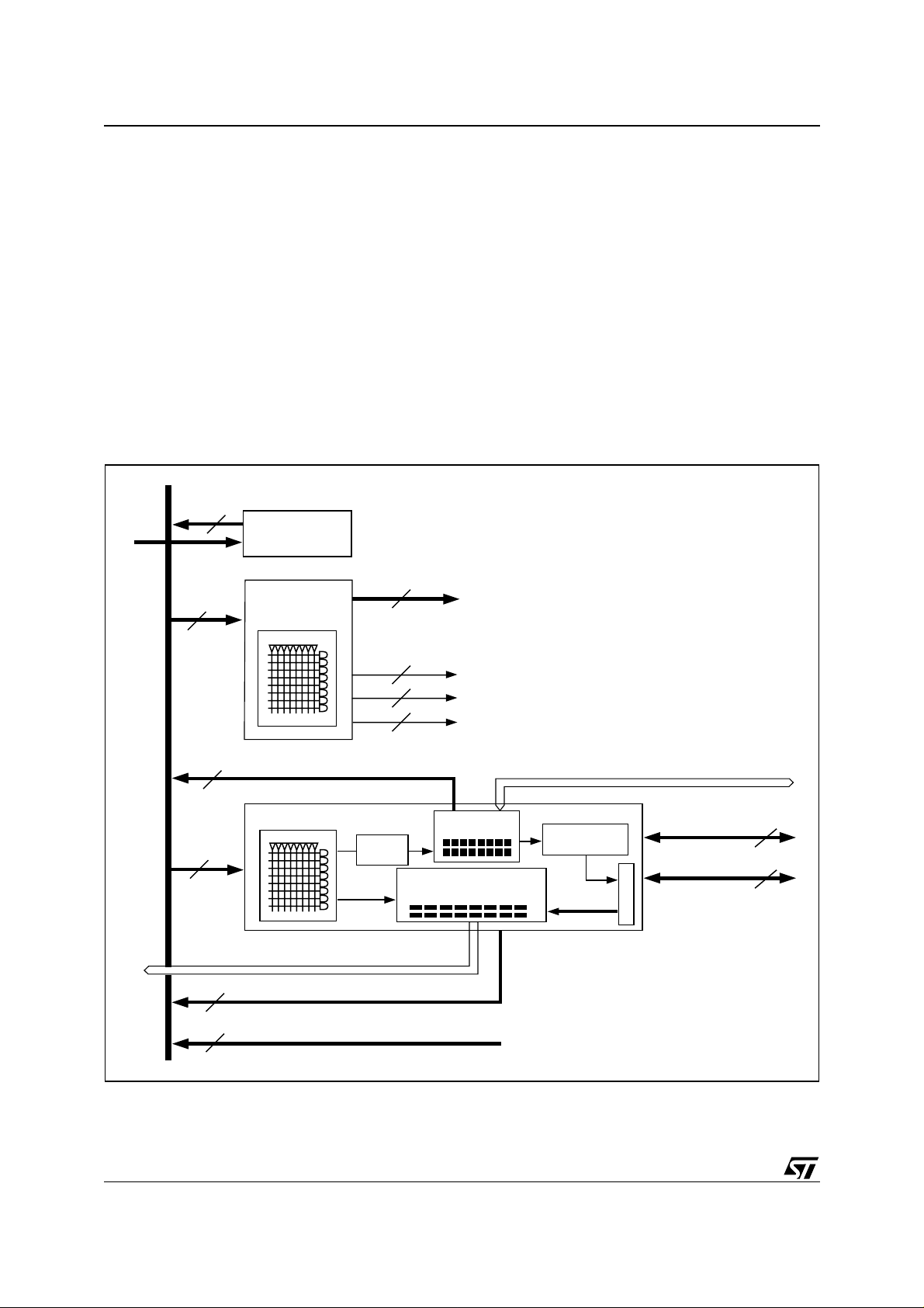
DSM2180F3
The DPLD performs address decoding, and generates select signals for internal and external components, such as memory, registers, and I/O ports.
The DPLD can generates External Chip Select
(ECS0-ECS2) signals on Port D.
The CPLD can be used for logic functions, such as
loadable counters and shift registers, state machines, and encoding and decoding logic. These
logic functions can be constructed using the 16
Output Macrocells (OMC), 16 Input Macrocells
(IMC), and the AND Array.
The AND Array is used to form product terms.
These product terms are configured from the logic
definition entered in PSDsoft Express. An Input
Bus consisting of 64 signals is connected to the
PLDs. Input signals are shown in Table 9.
Figure 13. PLD Diagram
8
Data
Bus
64
PAGE
REGISTER
DECODE PLD
(DPLD)
8
Turbo Bit. The PLDs in the device can minimize
power consumption by switching off when inputs
remain unchanged for an extended t ime of about
70 ns. Resetting the Turbo bit to 0 (Bit 3 of the
PMMR0 register) a utomatically places the PLDs
into standby if no inputs are changing. Turning the
Turbo mode off increases propagation delays
while reducing power consumption. Additionally,
five bits are available in the PMMR registers in
csiop
to block DSP control signals from entering
the PLDs. This reduces po wer consumption and
can be used only when these DSP control signals
are not used in PLD logi c equations. Each of the
two PLDs has unique characteristics suited for its
applications. They are des cribed in the following
sect ions.
Flash Memory Selects
16
PLD INPUT BUS
64
Direct Macrocell Input to MCU Data Bus
16
3
Output Macrocell Feedback
CPLD
PT
ALLOC.
Input Macrocell and Input Ports
PORT D Inputs
1
3
1
16 Input Macrocell
(PORT B,C)
CSIOP Select
External Chip Selects to PORT D
JTAG Select
Direct Macrocell Access from MCU Data Bus
16 Output
Macrocell
Macrocell
Alloc.
I/O PORTS
MCELLAB
to PORT B
MCELLBC
to PORT B or C
8
8
AI04900B
26/63
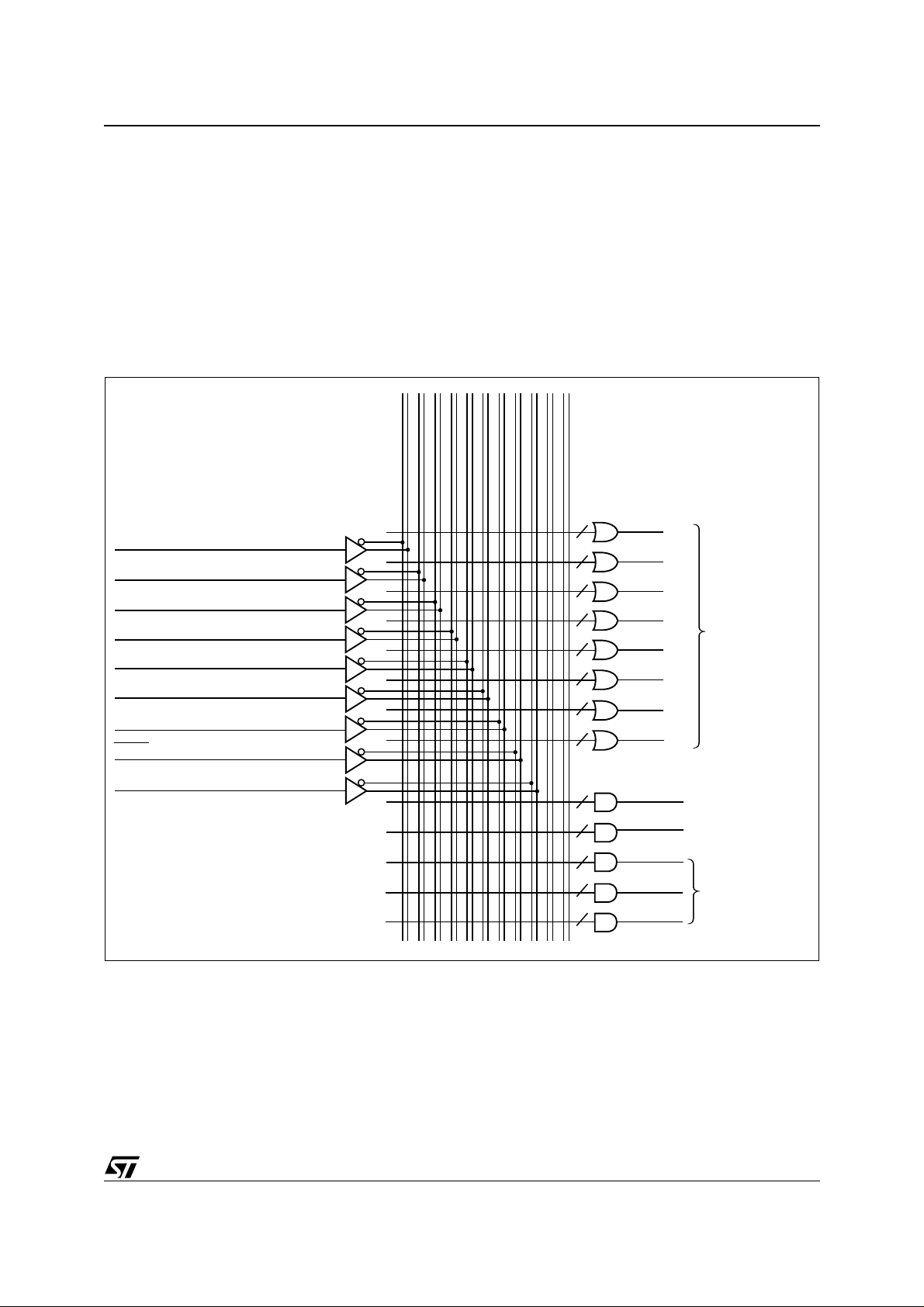
DECODE PLD (DPLD)
The DPLD, shown in Figure 14, is used for decoding the address for internal and external com ponents. The DPLD can be used to generate the
following decode signals:
■ 8 Flash memory Sector Select (
FS0-FS7
)
signals with three product terms each
Figure 14. DPLD Logic Array
DSM2180F3
■ 1 internal
and status registers (
of the block of 256 byte locations)
■ 1 JTAG Select signal (enables JTAG operations
on Port C when multiplexing JTAG signals with
general I/O signals)
■ 3 external chip select output signals for Port D
pins, each with one product term.
csiop
sele c t for DS M devi ce cont r o l
csiop
is the base address
I/O PORTS (PORT A,B,C)
MCELLAB.FB [7:0] (Feedback)
MCELLBC.FB [7:0] (Feedback)
PG0 -PG7
]
A[15:0
]
PD[2:0
CNTRL[2:0
RESET
RD_BSY
] (
Read/Write Control Signals)
(INPUTS)
(16)
(8)
(8)
(8)
(16)
(3)
(3)
(1)
(1)
3
3
3
3
3
3
3
3
1
1
1
1
1
CSIOP
JTAGSEL
ECS0
ECS1
ECS2
FS0
FS1
FS2
FS3
8 Flash Memory
Sector Selects
FS4
FS5
FS6
FS7
I/O Decoder
Select
JTAG ISP
External Chip Selects
to PORT D
AI04901
27/63

DSM2180F3
COMPLEX PLD (CPL D )
The CPLD can be used to implement system logic
functions, such as loadable counters and shift registers, system mailboxes, ha ndshaking protocols,
state machines, and random logic. See application
AN1171
note
ing PSDsoft Express.
As shown in Figure 15, the CPLD has the following
blocks:
■ 16 Input Macrocells (IMC)
■ 16 Output Macrocells (OMC)
■ Macrocell Allocato r
■ Product Term Allocator
■ AND Array capable of generating up to 130
product terms
Figure 15. Macrocell and I/O Port
for details on how to specify logic us-
■ Two I/O Ports.
Each of the blocks are described in the sections
that fo llow.
The Input Macrocells (IMC) and Output Macrocells
(OMC) are connected t o the device internal data
bus and can be directly accessed by the DSP. This
enables the DSP software to load data into the
Output Macroc ells (OMC) or read dat a from both
the Input and Output Macrocells (IMC and OMC).
This feature allows efficient implementation of system logic and eliminat es the need to connec t the
data bus to the AND Array as required in most
standard PLD macro cell architectures.
PLD INPUT BUSPLD INPUT BUS
AND ARRAY
Product Terms
from other
MacrocellS
CPLD Macrocells
PRODUCT TERM
ALLOCATOR
UP TO 10
PRODUCT TERMS
POLARITY
SELECT
PT
CLOCK
GLOBAL
CLOCK
CLOCK
SELECT
PT CLEAR
PT Output Enable (OE
Macrocell Feedback
I/O Port Input
PT INPUT LATCH GATE/CLOCK
PT PRESET
MUX
MCU DATA IN
PR DI LD
D/T
D/T/JK FF
SELECT
CK
)
DSP ADDRESS / DATA BUS
MCU LOAD
MUX
Q
COMB.
/REG
SELECT
CL
DATA
LOAD
CONTROL
Macrocell
Out to
MCU
Macrocell
I/O Port
Alloc.
CPLD
OUTPUT
to
TO OTHER I/O PORTS
I/O PORTS
LATCHED
ADDRESS OUT
DATA
D
Q
WR
CPLD OUTPUT
PDR
INPUT
Q
D
DIR
REG.
WR
Input Macrocells
MUX
MUX
SELECT
Q
QD
I/O Pin
D
G
AI04902B
Output Ma c rocell (OMC ). Eight of the Output
Macrocells (OMC) are connected to Port B pins
and are named as McellAB0-McellAB7. The other
eight Macrocells are connected to Ports B or C
pins and are named as McellBC0-McellBC7.
OMCs may be used for internal feedback only
(buried registers), or their outputs may be routed
to external Port pins.
28/63
The Output Macrocell (OMC) architecture is
shown in Figure 17. As shown in the figure, there
are native product terms a vailable from the AND
Array, and borrowed product terms available (if
unused) from other Output Macrocells (OMC). The
polarity of the product term is controlled by the
XOR gate. The Out put Macrocell (OMC) c an implement either sequential logic, usin g the flip-flop
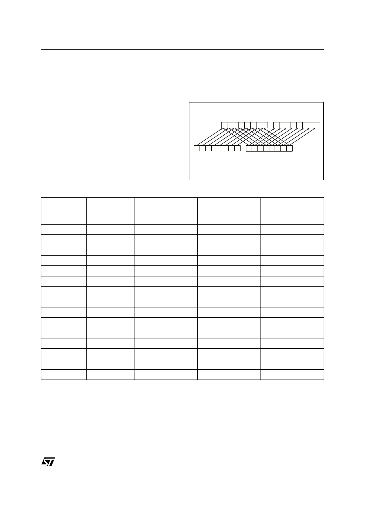
DSM2180F3
element, or combinatorial logic. The multiplexer
selects between the sequential or combinatorial
logic outputs. The multiplexer out put can drive a
port pin and has a feedback path to the AND Array
choosing pin functions in PSDsoft Express
Routing can occur on a bit-by-bit basis, spitting
assignment between the Ports. However, one
OMC can be routed to one Port pin only, not both.
inputs.
The flip-flop in the Output Macrocell (OMC) block
can be configured as a D, T, JK, or SR type in PSDsoft Express
TM
. The flip-flop’s clock, preset, and
Figure 16. OMC Allocator
clear inputs may be driven from a product term of
the AND Array. Alternatively, CLKIN (PD1) can be
01234567 01234567
used for the clock input to the flip-flop. The flip-flop
is clocked on the rising edge of CLKIN (PD1). The
preset and clear are active High inputs. Each clear
input can use up to two product terms.
Output Macrocell Allocator. Outputs of the 16
1
0
4567 32104567 32
OMCs (MCELLBC)OMCs (MCELLAB)
OMCs can be routed to a com bination of pins on
Port B or Port D as shown in Figure 16. The OMC
output pin is automatically determined by
Table 10. Output Macrocell Port and Data Bit Assignments
Output
Macrocell
McellAB0 Port B0 3 6 D0
McellAB1 Port B1 3 6 D1
Port
Assignment
Native Product Terms
Maximum Borrowed
Product Terms
Data Bit for Loading or
PORT C PINSPORT B PINS
Reading
AI04915
TM
.
McellAB2 Port B2 3 6 D2
McellAB3 Port B3 3 6 D3
McellAB4 Port B4 3 6 D4
McellAB5 Port B5 3 6 D5
McellAB6 Port B6 3 6 D6
McellAB7 Port B7 3 6 D7
McellBC0 Port B0 or C0 4 5 D0
McellBC1 Port B1 or C1 4 5 D1
McellBC2 Port B or, C2 4 5 D2
McellBC3 Port B3 orC3 4 5 D3
McellBC4 Port B4 orC4 4 6 D4
McellBC5 Port B5 or C5 4 6 D5
McellBC6 Port B6 orC6 4 6 D6
McellBC7 Port B7 orC7 4 6 D7
Product Term Al lo c at or. The CPLD has a Product Term Allocator. PSDsoft Express
TM
uses the
Product Term Allocator to borrow and plac e product terms from one Macrocell to another. This happens automatically in PSDsoft Express
TM
, but
understanding how allocation works will help you if
your logic design does not “f it”, in which c ase y ou
may try selecting a different pin or different OM C
where the allocation resources m ay di ffer and the
design will then fit. The f ollowing list summarizes
how product terms are allocated:
■ McellAB0-McellAB7 all have three native
product terms and may borrow up to six more
■ McellBC0-McellBC3 all have four native product
terms and may borrow up to five more
■ McellBC4-McellBC7 all have four native product
terms and may borrow up to six more.
29/63
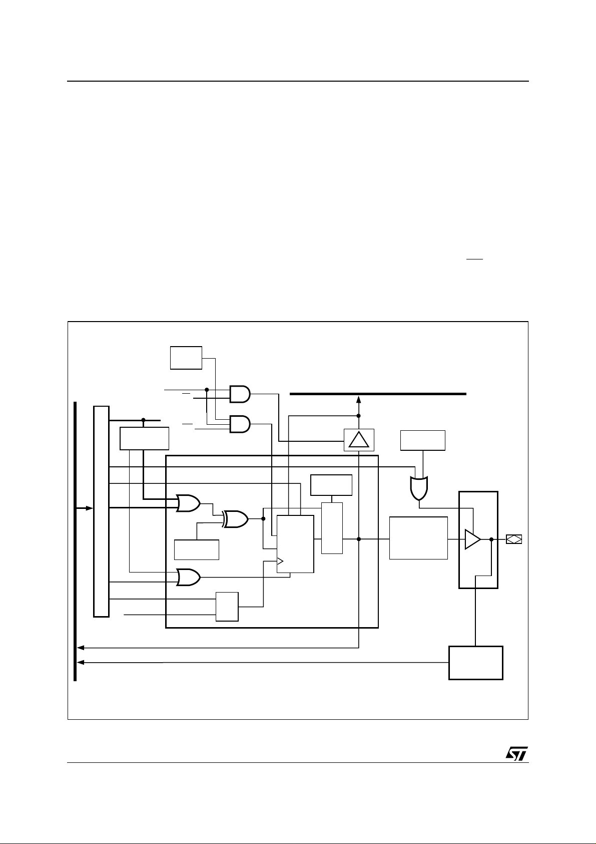
DSM2180F3
Each Macrocell may only borrow product terms
from certain other Macrocells. Product terms already in use by one Macrocell are not available for
another Macrocell. Product term allocation does
not add any propagation delay to the logic.
If an equation requires more product terms than
are available to it through product term allocation,
then “external” product terms are required, which
consumes other Output Macrocells (OMC). This is
called product term expansion and also happens
automatically in PSDsoft Express
TM
as needed.
Product tern expansion causes additional propagation delay because an OMC is consumed by the
expansion and it’s output is rerouted (or fed back)
into the AND array.
You can examine the fitter report generated by
PSDsoft Express to see resulting product term allocation and product term expansion.
Figure 17. CPLD Output Macrocell
MASK
REG.
Output Macrocell CS
RD
Loading and Reading the Output Macrocells
(OMCs). Each of the two OMC blocks (8 OMCs
each) occupies a memory location in the DSP ad-
csiop
dress space, as defined in the
block
MCELLAB0-7 and MCELLBC0-7 (see Table 4).
The flip-flops in each of the 16 OMCs can be loaded from the data bus by a DSP. Loading the OMCs
with data from the DSP takes priority over internal
functions. As such, the preset, clear, and clock inputs to the flip-flop can be overridden by the DSP.
The ability to load the flip-flops and read them
back is useful in such applications as loadable
counters and shift registers, mailboxes, and handshaking protocols.
Data is loaded into the Output Macrocells (OMC)
on the trailing edge of Write Strobe (WR
INTERNAL DATA BUS
D[7:0
]
, CNTL0).
AND ARRAY
PLD INPUT BUS
PT CLK
CLKIN
PT
Allocator
PT
PT
PT
WR
ENABLE (.OE
PRESET(.PR
POLARITY
SELECT
CLEAR (.RE
Feedback (.FB
Port Input
MUX
Direction
Register
)
)
LD
IN
)
)
PRDIN
Q
CLR
Programmable
FF (D/T/JK /SR
COMB/REG
SELECT
MUX
)
Macrocell
Allocator
Port
Driver
Input
Macrocell
I/O Pin
AI04903B
30/63
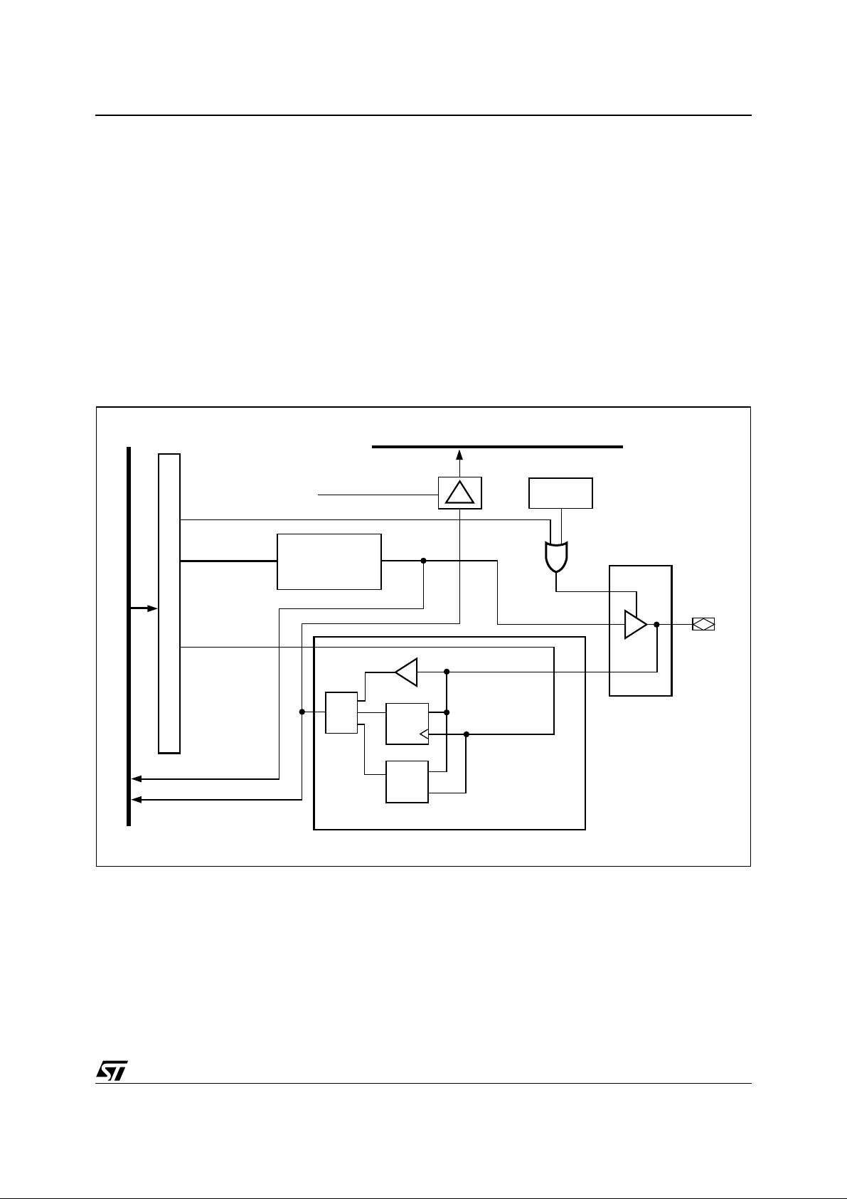
DSM2180F3
The OMC Mask Register. There is one Mask
Register for each of the two groups of eight Output
Macrocells (OMC). The Mask Registers can be
used to block the loading of data to individual Output Macrocells (OMC). The def ault value for the
Mask Registers is 00h, which allows loading of the
Output Macrocells (OMC ). When a given bit in a
Mask Register is set to a 1, the DSP is blocked
from writing to the associated Ou tput Macrocells
(OMC). For example, suppose McellAB0-3 are being used for a state machi ne. You would not want
a DSP write to McellAB to overwrite the state machine registers. Therefore, you would want to load
the Mask Register for McellAB (Mask Macrocell
AB) with the value 0Fh.
Figure 18. Input Macrocell
INPUT MACROCELL_ RD
ENABLE (.OE
PT
)
OUTPUT
Macrocells BC
AND
Macrocells AB
The Output Enable of the OMC. The Output
Macrocells (OMC) block can be connected to an I/
O port pin as a P LD output. The output enab le of
each port pin driver is controlled by a single product term from the AND Array, ORed with the Direction Register output. The pin is enabled upon
Power-up if no output enable equation is defined
and if the pin is declared as a PLD output in PSDsoft Express.
If the Output Macrocell (OMC) output is specified
as an internal node and not as a port pin output in
the PSDsoft Express, then the port pin can be
used for other I/O functions. The internal node
feedback can be routed as an input to the AND Array.
INTERNAL DATA BUS
DIRECTION
REGISTER
D[7:0
]
AND ARRAY
PT
PLD INPUT BUS
MUX
Feedback
Q
D FF
Q
LATCH
Input Macrocells (IMC). The CPLD has 16 Input
Macrocells (IMC), one for each pin on Ports B and
C. The architecture of the IMCs is shown in Figure
18. The IMCs are individually configurable, and
can be used as a latch, a register, or t o pass incoming Port signals prior to driving them onto the
PLD input bus. This is useful for sampling and debouncing inputs to the AND array (keypad i nput s,
etc.). Additionally, the outputs of the IMCs can be
read by the DSP asynchronously at any time
I/O Pin
Port
Driver
D
D
G
PT
Input Macrocell
AI04904B
through the internal data bus using the csiop register block (see Table 4).
The enable fo r the latch and c lock f or the regi ster
are driven by a product term from the CPLD. Each
product term output is used to latch or clock four
IMCs. Port inputs 3-0 can be controlled by one
product term and 7-4 by another.
Configurations for the IMCs are specified by equations specified in PSDs oft Express. See Application note
AN1171
.
31/63

DSM2180F3
DSP Bus Interface
The “no-glue logic” DSP Bus Interface allows direct connection. DSP address, data, and control
signals connect directly to the DSM device. See
Figure 6 for typical connections.
DSP address, data an d cont rol sig nals a re rout ed
csio p
to Flash memory, I/O control (
), OMCs, and
IMCs within the DMS. The DSP address range for
each of these components is specified in PSDsoft
Express
TM
.
I/O Po r t s
There are three programma ble I/O ports: P orts B,
C, and D. Each of the ports is eight bits except Port
D, which is 3 bits. Each port pin is individually user
configurable, thus allowing multiple functions per
port. The ports are configured using PSDsoft Ex-
Figure 19. Gene ral I/O P ort A rchi te cture
DATA OUT
REG.
WR
Macrocell Outputs
EXT CS
DQ
READ MUX
TM
press
in the
or by the DSP writing to on-chip registers
csiop
block.
The topics discussed in this section are:
■ General Port architectur e
■ Port operating modes
■ Port Configuration Registers (PCR)
■ Port Data Registers
■ Individual Port functionality.
General Port Architecture. The general architecture of the I/O Port block is shown in Figure 19.
Individual Port architectures are shown in Figure
20 to Figure 23. In general, once the purpose for a
port pin has been defined in PSDsoft Express
that pin is no longer available for other purposes.
Exceptions are noted.
DATA OUT
OUTPUT
MUX
PORT PIN
TM
,
P
INTERNAL DATA BUS
WR
ENABLE PRODUCT TERM (.OE
D
B
DIR REG.
DQ
CPLD-INPUT
DATA IN
)
As shown in Figure 19, the ports contain an output
multiplexer whose select signals are driven by the
configuration bits determined by PSDsoft Express.
Inputs to the multiplexer include the following:
■ Output data from the Data Out register (for MCU
I/O mode)
■ CPLD Macrocell output (OMC)
OUTPUT
SELECT
ENABLE OUT
Input
Macrocell
AI04905B
■ External Chip Selects ESC0-2 from the DPLD to
Port D pins only.
The Port Data Buffer (PDB) is a tri-state buffer that
allows only one source at a time to be read by the
DSP. The Port Data Buffer (PDB) is connected to
the Internal Data Bus for feedback and can be
read by the DSP. The Data Out and Macrocell out-
32/63

DSM2180F3
puts, Direction Registers, and port pin input are all
connected to the Port Data Buffer (PDB).
The Port pin’s tri-state output driver enable is controlled by a two input OR gate whose inputs come
from the CPLD AND Array enable product term
and the Direction Register. If the enable product
term of any of the Array outputs are not defined
and that port pin is not defined as a CPLD ou tput
in PSDsoft Exp re s s
TM
, then the Direction Register
has sole control of the bu ffer that drives the port
pin.
The contents of these registers can be altered by
the DSP. The Port Data Buffer (PDB) feedback
path allows the DSP to check the contents of the
registers.
bouncing), as transparent latches, or direct inp uts
to the PLDs. The registers and latches are clocked
by a product term from the PLD AND Array. The
outputs from the IMCs drive the PLD input bus and
can be read by the DSP. See the sec tion entitled
“Input Macrocell”, on page 31.
Port Operat in g Mo des
The I/O Ports have several modes of operation.
Modes are defined using PSDsoft Express
then runtime control from the DSP can occur using
the registers in the
Note
AN1171
for more detail.
csiop
block. See Application
Table 11 summ arizes which modes are available
on each port. Each of the port operating modes
are described in the following sections.
Ports B, and C have embedded IMCs. The IMCs
can be configured as registers (for sampling or de-
Table 11. Port Operating Modes
Port Mode Port B Port C Port D
MCU I/O Yes Yes Yes
PLD I/O
McellAB Outputs
McellBC Outputs
Additional Ext. CS Outputs
PLD Inputs
JTAG ISP No
Note: 1. Can be mul tiplexed wi th other I/O functions.
MCU I/O Mode. In the MCU I/O mode, the DS P
uses the I/O Ports block to expand its own I/O
ports. The DSP can read I/O pins, set the direction
of I/O pins, and change the state of I/O pins by accessing the registers in the
csiop
block. The
register definition and their addresses may be
found in Table 4.
The MCU I/O direction may be changed by writing
to the corresponding bit in the Direction Re gister,
or by the output enable product term. When the pin
is configured as an output, the content of the Data
Out Register drives the pin. When configured as
an input, the DSP can read the port input through
the Data In buffer. See Figure 19.
PLD I/ O Mode. Inputs from Ports B and C to either PLD (DPLD or CPLD) come through IMCs. Inputs from Port D to either PLDs are routed directly
in and do not use IMCs. Outputs from the CPLD to
Port B come from the OMC gro up MCELLAB0-7.
Outputs from the CPLD to Port C come from OMC
group MCELLBC0-7. Outputs from the DPLD to
Port D come from the external chip select logic
block ECS0-2.
All PLD outputs may be tri-stated at the Port pins
with a control signal. This output enable control
signal can be defined by a product term from the
Yes
Yes
No
Yes
csiop
No
Yes
No
Yes
1
Yes
PLD, or by resetting the corresponding bit in the
Direction Register to 0. The corres ponding bit in
the Direction Register must not be set to logic 1 by
the DSP if the pin is defined for a PLD input signal
in PSDsoft Express. The PLD I/O mode is defined
in PSDsoft Express by specifying PLD equations.
JTAG In-System Programming (ISP). Some of
the pins on Port C are based on the IEEE 1194.1
JTAG specification and is used for In-System Programming (ISP). You can multiplex the function of
these Port C JTAG pins w ith other functions. ISP
is not performed very frequently in the life of the
product, so multiplexing these pin’s functions with
general purpose I/O functions gives more utility
from Port C. See the section entitled “Programming In-Circuit Using JTAG ISP” , and Applicat ion
Note
AN1153
.
Port Configuration Registers (PCR). Each Po rt
has a set of Port Configuration Registers (PCR)
used for configuration of the pins. The contents of
the registers can be accessed by the DSP through
normal read/write bus cycles o f the
csiop
listed in Table 4.
The pins of a port are individually configurable and
each bit in the register controls its respective pin.
For example, Bit 0 in a register refers to Bit 0 of its
No
No
Yes
Yes
No
TM
, and
registers
33/63

DSM2180F3
port. The three Port Configuration Registers
(PCR), are shown in Table 12. Default is logic 0.
Table 12. Port Configuration Registers (PCR)
Register Name Port D SP Access
Data In B,C,D Read
Data Out B,C,D Write/Read
Direction B,C,D Write/Read
1
Drive Select
Note: 1. See Table 16 for Driv e Register bit d ef inition.
B,C,D Write/Read
Data In Register. The DSP may read the Data In
csio p
registers in the
block at any tim e to determine the logic state of a Port pin. This will be the
state at the pin regardless of whether it is driven by
a source external to the DSM or driven internally
from the DSM device. Reading a logic zero for a bit
in a Data In register means the corresponding Port
pin is also at logic zero. Reading logic one means
the pin is logic one. Each bit in a Data In register
corresponds to an individual Port pin. For a given
Port, bit 0 in a Data In register corresponds to pin
0 of the Port. Example, bit 0 of the Data I n register
for Port B corresponds to Port B pin PB0.
Data Out Register. The DSP may write (or read)
the Data Out register in the
csiop
block at any
time. Writing the Data Out register will change the
logic state of a Port pin only if it is not driven or
controlled by the CPLD. Writing a logic zero to a bit
in a Data Out register will force the corresponding
Port pin to be logic zero. Writing logic one will drive
the pin to logic one. Each bit in the Data Out registers correspond to Port pins the same way as the
Data In registers described above. When some
pins of a Port are driven by the CP LD, writing to
the corresponding bit in a Data Out register will
have no effect as the CPLD overrides the Data Out
register.
Direction Register. The Direction Register, in
conjunction with the output enable (except for Port
D), controls the direction of data flow in the I/O
Ports. Any bit set to 1 in the Direction Register
causes the corresponding pin to be an output, and
any bit set to 0 causes it to be an input. The default
mode for all port pins is input.
Table 13. Port Pin Direction Control, Output
Enable P.T. Not Defined
Direction Register Bit Port Pin Mode
Table 14. Port Pin Direction Control, Output
Enable P.T. Defined
Direction
Register Bit
0 0 Input
0 1 Output
1 0 Output
1 1 Output
Output Enable
P.T.
Port Pin Mode
Table 15. Port Direction Assignment Example
Bit 7 Bit 6 Bit 5 Bit 4 Bit 3 Bit 2 Bit 1 Bit 0
0 0 0 0 0 1 1 1
Figure 20 and Figure 21 s how the Port Architecture diagrams for Ports B and C, respectively. The
direction of data flow for Ports B, and C are controlled not only by the direction register, but also by
the output enable product term from the PLD AND
Array. If the output enable product term is not active, the Direction Register has sole control of a
given pin’s direction.
An example of a configuration for a Port with the
three least significant bits set to output and the remainder set to input is shown in Tab le 15. Since
Port D only contains three pins (shown i n Figure
23), the Direction Register for Port D has only the
three least significant bits active.
Drive Select Register. The Drive Select Register
configures the pin driver as Open Drain or CMOS
(standard push/pull) for some port pins, and controls the slew rate for the other port pins. An external pull-up resistor should be used for pins
configured as Open Drain. Open Drain outputs are
diode clamped, thus t he maximum vol tage on an
pin configured as Open Drain is Vcc + 0.7V.
A pin can be configured as Open Drain if its corresponding bit in the Drive Select Register is set to a
1. The default pin drive is CMOS.
Note that the slew rate is a measurement o f the
rise and fall times of an output. A higher slew rate
means a faster output response and may create
more electrical noise. A pin operates in a high slew
rate when the corresponding bit in the Drive Register is set to 1. The default rate is standard slew.
Table 16 shows the Drive Register for Ports B , C,
and D. It summarizes which pins can be configured as Open Drai n outputs and which pins the
slew rate can be set for.
0 Input
1 Output
34/63

Table 16. Drive Register Pin Assignment
Drive
Register
Port B
Port C
Port D
Note: 1. NA = Not Applicable.
Bit 7 Bit 6 Bit 5 Bit 4 Bit 3 Bit 2 Bit 1 Bit 0
Open
Drain
Open
Drain
1
NA
Open
Drain
Open
Drain
1
NA
Open
Drain
Open
Drain
1
NA
Figure 20. Port B Structure
DATA OUT
REG.
WR
MACROCELL OUTPUTS
DQ
Open
Drain
Open
Drain
1
NA
Slew
Rate
Open
Drain
NA
DATA OUT
DSM2180F3
Slew
Rate
Open
Drain
1
Slew
Rate
OUTPUT
MUX
Slew
Rate
Open
Drain
Slew
Rate
Slew
Rate
Open
Drain
Slew
Rate
PORT B
PIN
READ MUX
P
D
B
INTERNAL DATA BUS
DIR REG.
WR
ENABLE PRODUCT TERM (.OE
DQ
)
CPLD-INPUT
Port B – Functionality and Structure
Port B can be configured to perform one or more
of the following functions:
■ MCU I/O Mode
■ CPLD Output – Macrocells McellAB7-McellAB0
can be connected to Port B. McellBC7McellBC0 can be connected to Port B or Port C.
OUTPUT
DATA IN
■ CPLD Input – Via the Input Macrocells (IMC).
■ Open Drain/Slew Rate – pins PB3-PB0 can be
SELECT
ENABLE OUT
Macrocell
Input
AI04906B
configured to fast slew rate, pins PB7-PB4 can
be configured to Open Drain Mode.
35/63
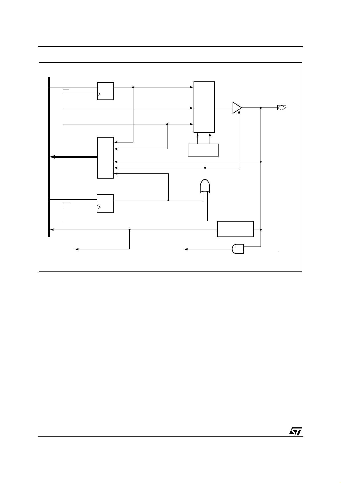
DSM2180F3
Figure 21. Port C Structure
DATA OUT
REG.
WR
DQ
DATA OUT
MCELLBC[7:0
INTERNAL DATA BUS
WR
ENABLE PRODUCT TERM (.OE
]
READ MUX
P
D
B
DIR REG.
DQ
CPLD-INPUT
JTAG ISP
DATA IN
)
OUTPUT
MUX
OUTPUT
SELECT
ENABLE OUT
INPUT
MACROCELL
JTAG ISP
PORT C PIN
CONFIGURATION
BIT
AI04907
Port C – Functionality and Structure
Port C can be configured to perform one or more
of the following functions (see Figure 21):
■ MCU I/O Mode
■ CPLD Output – McellBC7-McellBC0 outputs
can be connected to Port B or Port C.
■ CPLD Input – via the Input Macrocells (IMC)
36/63
■ In-System Programming (ISP) – JTAG port can
be enabled for programming/erase of the
device. (See the section entitled “Programming
In-Circuit Using JTAG ISP”, and Application
Note
AN1153
, for more information on JTAG
programming.)
■ Open Drain – Port C pins can be configured in
Open Drain Mode

Figure 22. Port D Structure
WR
DATA OUT
REG.
DQ
DSM2180F3
DATA OUT
]
ECS[2:0
READ MUX
P
D
DATA IN
INTERNAL DATA BUS
WR
B
DIR REG.
DQ
Port D – Functionality and Structure
Port D has three I/O pins. See Figure 22 a nd Figure 23. Port D can be configured to perform one or
more of the following functions:
■ MCU I/O Mode
■ DPLD Output – External Chip Selects, ECS0-2
does not consume OMCs
■ CPLD Input – direct input to the CPLD, does not
use IMCs
■ Slew rate – pins can be set up for fast slew rate
Port D pins can be configured in PSDsoft as input pins for other dedicated functions:
■ CLKIN (PD1) as input to the OMCs Flip-flops
OUTPUT
MUX
OUTPUT
SELECT
ENABLE PRODUCT
TERM (.OE)
CPLD-INPUT
■ PSD Chip Select In put (CSI, PD2). Driving th i s
PORT D PIN
AI02889
signal logic High disables the Flash memory,
putting it in standby mode.
External Chip Select. The DPLD also provides
three External Chip Select outputs (ESC0-2) on
Port D pins that can be used to select external devices as defined in PS Dsoft E xpress . Ea ch E xternal Chip Select consists of one product term that
can be configured act ive High or Low. The output
enable of the pin is cont rolled by either t he ou tput
enable product term or the Direction Register.
(See Figure 23.) External Chip Selects f or Port D
pins do not consume OMC s. External chip select
outputs can also come from the CPLD if c hip select equations are specified in PSDsoft Express for
Ports B or C.
37/63

DSM2180F3
Figure 23. Port D External Chip Select Signals
PLD INPUT BUS
PT0
POLARITY
CPLD AND ARRAY
PT1
POLARITY
PT2
POLARITY
BIT
BIT
BIT
ENABLE (.OE)
ENABLE (.OE)
ENABLE (.OE)
ECS0
ECS1
ECS2
DIRECTION
REGISTER
DIRECTION
REGISTER
DIRECTION
REGISTER
PD0 PIN
PD1 PIN
PD2 PIN
AI02890
38/63

POWER MANAGEMENT
The device offers configurab le power saving options. These options may be used individually or in
combinations, as follows:
■ All memory blocks in the device are b uilt with
zero-power management technology. Zeropower technology puts the memories into
standby mode when address/data inputs are
not changing (zero DC current). As soon as a
transition occurs on an input, the affected
memory “wakes up”, changes and latches its
outputs, then goes back to standby. The
designer does
not
have to do anything special to
achieve memory standby mode when no inputs
are changing—it happens automat ically.
Both PLDs (DPLD and CPLD) are also Zeropower, but this is not the default operation. The
DSP must set a bit at run-time to achieve Zeropower as described next.
■ The PMMR registers can be written by the DSP
at run-time to manage power. The device has a
Turbo bit in the PMMR0 register. This bit can be
set to turn the Turbo mode off (the default is with
Turbo mode turned on). While Turbo mode is
off, the PLDs can achieve standby current when
no PLD inputs are changing (zero DC current).
Even when inputs do change, significant power
can be saved at lower frequencies (AC current),
DSM2180F3
compared to when Turbo mode is on. When the
Turbo mode is on, there is a significant DC
current component and the AC component is
higher.
Further significant power savings can be
achieved by blocking s ignals that are not used
in DPLD or CPLD logic equations. The “blocking
bits” in PMMR registers can be set to logic 1 by
the DSP to block designated signals from reaching both PLDs. Current consumption of the
PLDs is directly related to the composite frequency of the changes on their input s (see F igure 25), so blocking unused PLD inputs can
significantly lower PLD operating frequency and
power consumption. The DSP a lso has the option of blocking certain PLD input when not
needed, then letting them pass for when needed
for specific logic operations. Table 17 and Table
18 define the PMMR registers.
■ PSD Chip Sel e ct Input (CSI, PD2) can be used
to disable the internal memories and
registers, placing them in standby mode even if
inputs are changing. This feature does not block
any internal signals or disable the PLDs. There
is a slight penalty in memory access time when
PSD Chip Select In put (CSI
, PD2 ) makes i ts
initial transition from deselected to selected.
csiop
Table 17. Power Management Mode Registers PMMR0
Bit 0 X 0 Not used, and should be set to zero.
Bit 1 X 0 Not used, and should be set to zero.
Bit 2 X 0 Not used, and should be set to zero.
Bit 3 PLD Turbo
Bit 4 PLD Array clk
Bit 5 PLD MCell clk
Bit 6 X 0 Not used, and should be set to zero.
Bit 7 X 0 Not used, and should be set to zero.
Note: 1. The bits of this register are clear ed to zero following Powe r-up. Subsequent Reset (Reset) pulses do not clear the regis ters.
0 = on PLD Turbo mode is on
1 = off PLD Turbo mode is off, saving power.
0 = on
1 = off CLKIN (PD1) input to PLD AND Array is blocked, saving power.
0 = on CLKIN (PD1) input to the PLD Macrocells is passed onto PLDs.
1 = off CLKIN (PD1) input to PLD Macrocells is blocked, saving power.
CLKIN (PD1) input to the PLD AND Array is passed onto PLDs. Every change of
CLKIN (PD1) Powers-up the PLD when Turbo bit is 0.
1
39/63

DSM2180F3
PLD Powe r M anagement
The power and speed of the PLDs are controlled
by the Turbo bit (bit 3) in the PMMR0. By set ting
the bit to 1, the Turbo mode is off and the PLDs
consume the specified stand-by current when the
inputs are not switching for an extended time of
70 ns. The propagation delay time is increased by
10 ns after the Turbo bit is set to 1 (turned off)
of less than 15 MHz. When the Turbo bit is reset to
0 (turned on), the PLDs run at full power and
speed. The Turbo bit affects the PLD’s DC power,
AC power, and propagation delay.
Blocking MCU control signals with the bits of the
PMMR registers can further reduce PLD AC power
consumption by lowering the effective composite
frequency of inputs to the PLDs.
when the inputs change at a composite frequency
Table 18. Power Management Mode Registers PMMR2
Bit 0 X 0 Not used, and should be set to zero.
Bit 1 X 0 Not used, and should be set to zero.
Bit 2
Bit 3
Bit 4
Bit 5
Bit 6
PLD Array
CNTL0
PLD Array
CNTL1
PLD Array
CNTL2
PLD Array
PD0
PLD Array
PC7
0 = on Cntl0 input to the PLD AND Array is passed onto PLDs.
1 = off Cntl0 input to PLD AND Array is blocked, saving power.
0 = on Cntl1 input to the PLD AND Array is passed onto PLDs.
1 = off Cntl1 input to PLD AND Array is blocked, saving power.
0 = on Cntl2 input to the PLD AND Array is passed onto PLDs.
1 = off Cntl2 input to PLD AND Array is blocked, saving power.
0 = on PD0 input to the PLD AND Array is passed onto PLDs.
1 = off PD0 input to PLD AND Array is blocked, saving power.
0 = on PC7 input to the PLD AND Array is passed onto PLDs.
1 = off PC7 input to PLD AND Array is blocked, saving power.
1
Bit 7 X 0 Not used, and should be set to zero.
Note: 1. The bits of this register are clear ed to zero following Powe r-up. Subsequent Reset (Reset) pulses do not clear the regis ters.
from the PLD AND A rray or the Macrocells block
PSD Chip Select Input (CSI, PD2)
PD2 of Port D can b e configured in PSDsoft Express as PSD Chip Select Input (
CSI). When Low,
the signal selects and enables the internal Flash
memory and I/O blocks for Read or Write operations involving the device. A High on PSD Chip Select Inp ut (
CSI, PD2) disa bles the Flash memory
and reduces the device power consumption. However, the PLD and I/O signals remain operational
when PSD Chip Select Input (
CSI, PD2) is High.
There may be a timing pena lty when using PSD
Chip Select Input (
CSI, PD2) depending on the
speed grade of the device that you are using. See
the timing parameter t
in Table 31.
SLQV
Input Clock. The device provides the option to
block CLKIN (PD1) from reaching the PLDs to
save AC power consumpt ion. CLKIN (PD1) is an
input to the PLD AND Array and the OMCs.
If CLKIN (PD1) is not being use d as part of the
PLD logic equation, the clock should be blocked to
by setting bits 4 or 5 to a 1 in PMMR0.
Input Cont rol Signals. The device provides the
option to block the input control signals (CNTL0,
CNTL1, CNTL2, PD0, and PC7) from reaching the
PLDs to save AC power consumption. These control signals are inputs to the PLD AND Array. If any
of these are not being used as part of the PLD logic equation, these control signals should be disabled to save AC power. They are disconnected
from the PLD AND Array by set ting bits 2, 3, 4, 5,
and 6 to a 1 in the PMMR2 register. Note: CNTL0
and CNTL1 (DSP
WR and DSP RD) are perma-
nently routed to the Flash m em ory array and cannot be blocked from the array by the PMMR
registers (that’s why WR and RD signals do not
have to be specified in PSDsoft Express for Flash
memory segmen t chip-select equations f or FS0 FS7). CNTL0 and CNTL1 are blocked from the
PLDs with PMMR registers bits when thes e signals are specifically used in logic equations specified in PSDsoft Expr e ss.
save AC power. CLKIN (PD1) is disconnected
40/63

Figure 24. Reset (RESET) Timing
DSM2180F3
V
CC
RESET
Power On Reset, Warm Reset, Power-down
Power On Reset. Upon Power-up, the device re-
quires a Reset (
RESET) pulse of duration t
after VCC is steady. During this time period, the device loads internal configurat ions, clears som e of
the registers and sets the Flash me mory into Operating mode. After the rising e dge of Reset (
SET), the device remains in the Reset mode for an
additional period, t
VCC(min)
t
NLNH-PO
Power-On Reset
, before the first memory ac-
OPR
t
OPR
NLNH-PO
RE-
t
NLNH
t
NLNH-A
Warm Reset
The Flash memory is reset to the Read Array
mode upon Power-up. Sector Select FS0-FS7
must all be Low, Write Strobe (
WR, CNTL0) High,
during Power On Reset for maximum security of
the data contents and to remove the possibi lity of
a byte being written on the first edge of Write
Strobe (
WR, CNTL0). Any Flash memory Write cy-
cle initiation is prevented automatically when V
is below V
LKO
.
cess is allowed.
Table 19. Status During Power-On Reset, Warm Reset and Power-down Mode
Port Configuration Power-On Reset Warm Reset Power-down Mode
MCU I/O Input mode Input mode Unchanged
PLD Output
Valid after internal PSD
configuration bits are
loaded
Valid
Depends on inputs to PLD
(addresses are blocked in
PD mode)
t
OPR
AI02866b
CC
Register Power-On Reset Warm Reset Power-down Mode
PMMR0 and PMMR2 Cleared to 0 Unchanged Unchanged
OMC Flip-flop status
All other registers Cleared to 0 Cleared to 0 Unchanged
Cleared to 0 by internal
Power-On Reset
Warm Reset. Once the device is up and running,
the device can be reset with a pulse of a m uch
shorter duration, t
. The same t
NLNH
OPR
period is
needed before the device is operational after
warm reset. Figure 24 shows the timing of the
Power-up and warm reset.
I/O Pin, Register and PLD Status at Reset. Table 19 shows the I/O pin, register and PLD status
during Power On Reset, warm reset and Powerdown mode. PLD output s are always v alid during
warm reset, and they are valid in Power On Reset
once the internal device Configuration bits are
loaded. This loading of the device is completed
typically long before t he V
ramps up to operat-
CC
ing level. Once the P LD is active, t he state of t he
outputs are determined by the PSDsoft Express
equations.
Depends on .re and .pr
equations
Depends on .re and .pr
equations
Programming In-Circuit using JTAG ISP
In-System Programming (ISP) can be pe rformed
through the JTAG signals on Port C. This serial interface allows programming of the entire DSM device or subsections (i.e. only Flash memory but not
the PLDs) without and participation of the DS P. A
blank DSM device soldered to a circuit board can
be completely programmed in 10 to 20 seconds.
The basic JTAG signals; TMS, TCK, TDI, and
TDO form the IEEE-1149.1 interface. The DSM
device does not implement the IEEE-1149.1
Boundary Scan functions. The DSM uses the
JTAG interface for ISP only. However, the DSM
device can reside i n a standard JTAG chain with
other JTA G device s as it w ill rema in in BYPASS
mode while other devices perform Boundary
Scan.
41/63

DSM2180F3
ISP programming time can be reduced as much as
30% by using two more signals on Port C, TSTAT
and TERR
See Table 20. The FlashLINK
in addition to TMS, TCK, TDI and TDO.
TM
JTAG program-
ming cable available from ST Microelectronics for
$59USD and PSDsoft Express software that is
available at no charge from www.psdst.com is all
that is needed to program a DSM device using the
parallel port on any PC or laptop.
By default, the four pins on Port C are enabled for
the basic JTAG signals TMS, TCK, TDI, and TDO
on a blank device (and as shipped from factory)
See Application Note
AN1153
for more details on
JTAG In-System Programming (ISP).
Standard JTAG Signals. The standard JTAG
signals (TMS, TCK, TDI, and TDO) can be enabled by any of three different conditions that are
logically ORed. W hen enabled, TDI, TDO, TCK,
and TMS are inputs, waiting for a JTAG serial
command from an external JTAG controller device
(such as FlashLINK or Automated Test Equipment). When the enabling c ommand is received,
TDO becomes an output and the JTAG channel is
fully functional inside the device. The same command that enables the JTAG channel may optionally enable the two additional JTAG signals,
TSTAT
and TERR.
The following symbolic logic equation specifies the
conditions enabling the four basic JTAG signals
(TMS, TCK, TDI, and TDO) on their respective
Port C pins. For purposes of discussion, the logic
label JTAG_ON is used. When JTAG_ON is true,
the four pins are enabled for JTAG operation.
When JTAG_ON is false, the four pins can be
used for general dev ice I/O as specified in PSDsoft Express. JTAG_ON can become true by any
of three different ways as shown:
JTAG_ON =
1. PSDsoft Express Pin Configuration -OR-
2. PSDsoft Express PLD equation -OR-
csiop
3. DSP writes to register in
block
Method 1 is most common. This is when the JTAG
pins are selected in PSDsoft Express to be “dedicated” JTAG pins. Th ey can always t ransmit and
receive JTAG information because they are “fulltime” JTAG pins.
Method 2 is used only when the JTAG pi ns are
multiplexed with general I/O functions. For designs that need every I/O pin, the JTA G pins m ay
be used for general I/O when they are not used for
ISP. However, when JTAG pins are multiplexed
with general I/O functions, the des igner must include a way to get the pins back into JTAG mode
when it is time for JTAG operations again. In this
case, a single PLD input from Ports B, C, or D
must be dedicated to switch the Port C pins from I/
O mode back to ISP mode at any time. It is recom-
mended to physically connect this dedicat ed PLD
input pin to the JEN\ output signal from the
Flashlink cable when multiplexing JTAG signals.
See Application Note
AN1153
for details.
Method 3 is rarely used to control JTAG pin operation. The DSP can set the port C pins to function
as JTAG ISP by setting the JTAG Enable bit in a
csiop
register of the
block, but as soon as the DSM
chip is reset, the csiop block registers are cleared,
which turns off the JTAG-ISP function. Controlling
JTAG pins using this method is not recommended.
Table 20. JTAG Port Signals
Port C Pin JTAG Signals Description
PC0 TMS Mode Select
PC1 TCK Clock
PC3 TSTAT
PC4 TERR
PC5 TDI Serial Data In
PC6 TDO Serial Data Out
JTAG Extensions. TSTAT
Status
Error Flag
and TERR are two
JTAG extension signals (must be used as a pair)
enabled by a command received over the four
standard JTAG signals (TMS, TCK, TDI, and
TDO) by PSDsoft Express. They are used to
speed Program and Erase cycles by indicating
status on device pins instead of having to scan the
status out serially using t he standa rd J TAG channel. See Application Note
indicates if an error has occurred when
TERR
AN1153
.
erasing a sector or program ming a byte in F lash
memory. This signal goes Low (active) when an
Error condition occurs.
TSTAT
scribed previously.
behaves the same as Ready/Busy de-
TSTAT is inactive logic 1 when
the device is i n Read mode (Flash memory contents can be read).
TSTAT is logic 0 when Flash
memory Program or Erase cycles are in progress.
TSTAT
and TERR can be configured as opendrain type signals with PSDsoft Express. This facilitates a wired-OR connection of T STAT
signals
from multiple DSM2180F3 devices and a wiredOR connection of TERR
signals from thos e sam e
devices. This is useful when severa l d evices are
“chained” together in a JTAG environment. PSDsoft Express puts TSTAT
and TERR signals to
open-drain by default. Click on 'Properties' in the
JTAG-ISP window of PSDsoft Express to change
to standard CMOS pu sh-pull. It is rec ommended
42/63

DSM2180F3
to use 10 kΩ pull-up resistors to VCC on all JTAGISP signals on your circuit board.
Initi a l D e liver y St a t e
When delivered from ST, the device has all bits in
the memory and PLDs erased to logic 1. The DSM
Configuration Register bits are set to 0. The code,
configuration, and PLD l ogic are loaded using the
programming procedure. The four basic JTAG ISP
signals (TCK, TMS, TDI, TDO) are ready for ISP
funct ion.
43/63
DSM2180F3
AC/DC PARAMETERS
These tables describe the AD and DC parameters
of the device:
❏ DC Electrical Specification
❏ AC Timing Specification
■ PLD Timing
– Combinatorial Timing
– Synchronous Clock Mode
– Asynchronous Clock Mode
– Input Macrocell Timing
■ DSP Timing
– Read Timing
–Write Timing
– Reset Timing
The following are issues concerning the parameters presented:
■ In the DC specification the supply current is
given for different modes of operation. Before
calculating the total power consumption,
determine the percentage of time that the
device is in each mode. Also, the supply power
is considerably different if the Turbo bit is 0.
■ The AC power component gives the PLD and
Flash memory a mA/MHz specification. Figure
25 show the PLD mA/MHz as a function of the
number of Product Terms (PT) used.
■ In the PLD timing parameters, add the required
delay when Turbo bit is 0.
Figure 25. PLD I
/Frequency Consumption
CC
110
100
90
80
70
60
– (mA)
50
CC
I
40
30
20
10
0
= 5V
V
CC
TURBO ON (100%)
TURBO OFF
010155 20 25
HIGHEST COMPOSITE FREQUENCY AT PLD INPUTS (MHz)
TURBO ON (25%)
TURBO OFF
PT 100%
PT 25%
AI02894
44/63

DSM2180F3
MAXIMUM RATIN G
Stressing the device ab ove the rating listed in the
Absolute Maximum Ratings table m ay cause permanent damage to the device. These are stress
ratings only and operation of the device at these or
any other conditions ab ove those i ndicated in t he
Operating sections of this specificat ion is not im-
Table 21. Absolute Maximum Ratings
Symbol Parameter Min. Max. Unit
T
STG
T
LEAD
V
IO
V
CC
V
PP
V
ESD
Note: 1. IPC/JEDEC J-STD-020A
2. JE DEC Std JESD22-A114A (C1=100 pF, R1 =1500 Ω, R2=500 Ω)
Storage Temperature –65 125 °C
Lead Temperature during Soldering (20 seconds max.)
Input and Output Voltage (Q = VOH or Hi-Z)
Supply Voltage –0.6 7.0 V
Device Programmer Supply Voltage –0.6 14.0 V
Electrostatic Discharge Voltage (Human Body model)
plied. Exposure to Absolute Maximum Rating conditions for extended periods may affect device
reliability. Refer also to the STMicroelectronics
SURE Program and ot her relevant quality documents.
1
–0.6 7.0 V
2
–2000 2000 V
235 °C
45/63

DSM2180F3
DC AND AC PARAMETERS
This section summarizes the operat ing and measurement conditions, and the DC and AC characteristics of the device. The parameters in t he DC
and AC Characteristic tables that follow are derived from tests performed under the Measure-
Table 22. Operating Conditions
Symbol Parameter Min. Max. Un it
ment Conditions summarized in the relevant
tables. Designers should chec k th at the o perat ing
conditions in their circuit matc h the meas urement
conditions when relying on the quoted parameters.
V
CC
T
A
Supply Voltage 4.5 5.5 V
Ambient Operating Temperature (industrial) –40 85 °C
Table 23. AC Measurement Conditions
Symbol Parameter Min. Max. Unit
C
L
Load Capacitance 30 pF
Input Rise and Fall Times 5 ns
Input Pulse Voltages
1.5
Input and Output Timing Reference Voltages 1.5 V
Note: 1. Output Hi-Z is defined as the point where data out is no longer driven.
Figure 26. AC Measurement I / O W aveform Figure 27. AC Mea surement Load Circuit
2.01 V
3.0V
0V
Test Point 1.5V
Device
Under Test
AI03103b
195 Ω
C
= 30 pF
L
(Including Scope and
Jig Capacitance)
AI03104b
V
Table 24. Capacitance
Symbol Parameter Test Condition
C
IN
C
OUT
C
VPP
Note: 1. Sampled only, not 100% tested.
2. Typical val ues are for T
46/63
Input Capacitance (for input
pins)
Output Capacitance (for input/
output pins)
Capacitance (for CNTL2/VPP)V
= 25°C and nominal supply voltages.
A
= 0V
V
IN
V
OUT
PP
= 0V
= 0V
Typ.
2
Max. Unit
46
812
18 25
pF
pF
pF

Table 25. AC Symbols for PLD Timing
Signal Letters Signal Behavior
A Address Input t Time
C CEout Output L Logic Level Low
D Input Data H Logic Level High
E E Input V Valid
N Reset Input or Output X No Longer a Valid Logic Level
P Port Signal Output Z Float
Q Output Data PW Pulse Width
RRD
Input (read)
DSM2180F3
S Chip Select Input, BMS
WWR
B
Input (write)
V
Output
STBY
, DMS, IOMS, or FSx
M Output Macrocell
Example: t
– Time from Address Valid to
AVWL
Write input Low.
Figure 28. Switching Waveforms – Key
WAVEFORMS
INPUTS OUTPUTS
STEADY INPUT
MAY CHANGE FROM
HI TO LO
MAY CHANGE FROM
LO TO HI
DON'T CARE
STEADY OUTPUT
WILL BE CHANGING
FROM HI TO LO
WILL BE CHANGING
LO TO HI
CHANGING, STATE
UNKNOWN
OUTPUTS ONLY
CENTER LINE IS
TRI-STATE
AI03102
47/63

DSM2180F3
Table 26. DC Characteristics
Symbol Parameter
Test Condition
(in addition to those in
Table 22)
Min. Typ. Max. Unit
V
V
V
V
V
HYS
V
LKO
V
V
V
OH1
I
IDLE
I
I
I
(DC)
I
CC
(Note
Input High Voltage
IH
Input Low Voltage
IL
Reset High Level Input Voltage
IH1
Reset Low Level Input Voltage
IL1
4.5 V < V
4.5 V < V
(Note
(Note
< 5.5 V
CC
< 5.5 V
CC
1
)
1
)
2
–0.5 0.8 V
0.8V
CC
–0.5
Reset Pin Hysteresis 0.3 V
VCC (min) for Flash Erase and
Program
Output Low Voltage
OL
Output High Voltage Except
OH
V
STBY
On
Output High Voltage V
Idle Current (VSTBY input)
Stand-by Supply Current
SB
for Power-down Mode
Input Leakage Current
LI
Output Leakage Current
LO
Operating
Supply
5
)
Current
On I
STBY
PLD Only
Flash memory
I
= 20 µA, VCC = 4.5 V
OL
I
= 8 mA, VCC = 4.5 V
OL
= –20 µA, VCC = 4.5 V
I
OH
= –2 mA, VCC = 4.5 V
I
OH
= 1 µA V
OH1
V
> V
CC
STBY
>VCC –0.3 V (Notes
CSI
V
< VIN < V
SS
0.45 < V
OUT
CC
< V
CC
PLD_TURBO = Off,
5
f = 0 MHz (Note
)
PLD_TURBO = On,
f = 0 MHz
During Flash memory Write/
Erase Only
2.5 4.2 V
0.01 0.1 V
0.25 0.45 V
4.4 4.49 V
2.4 3.9 V
– 0.8
STBY
–0.1 0.1 µA
2,3
)
75 200 µA
–1 ±.1 1 µA
–10 ±5 10 µA
0 µA/PT
400 700 µA/PT
15 30 mA
Read Only, f = 0 MHz 0 0 mA
VCC +0.5
VCC +0.5
0.2V
CC
–0.1
V
V
V
V
PLD AC Adder
(AC)
I
CC
(Note
Note: 1. Reset (Reset) has hy st eresis. V
Flash memory AC Adder 2.5 3.5
5
)
is valid at or below 0.2VCC –0.1. V
deselecte d .
2. CSI
3. PLD is in non-Turbo mode, and none of the inputs are switching.
4. Please see F i gure 25 for the PLD current c a l culation.
5. I
= 0 mA
OUT
IL1
48/63
4
(see note
is valid at or above 0.8VCC .
IH1
)
mA/
MHz

Table 27. CPLD Combina torial Timing
Symbol Parameter Conditions
-90
Min Max
Fast PT
Alloc
Turbo
Off
DSM2180F3
Slew
Rate
Unit
1
t
PD
t
EA
t
ER
t
ARP
t
ARPW
t
ARD
Note: 1. Fast Slew Rate output available on PB3-PB0, and PD2-PD0.
CPLD Input Pin/Feedback to
CPLD Combinatorial Output
CPLD Input to CPLD Output
Enable
CPLD Input to CPLD Output
Disable
CPLD Register Clear or Preset
Delay
CPLD Register Clear or Preset
Pulse Width
CPLD Array Delay Any Macrocell 16 Add 2 ns
25 Add 2 Add 10 Sub 2 ns
26 Add 10 Sub 2 ns
26 Add 10 Sub 2 ns
26 Add 10 Sub 2 ns
20 Add 10 ns
49/63

DSM2180F3
Table 28. CPLD Macrocell Synchrono us Clock Mode Timing
-90
Symbol Parameter Conditions
Min Max
Fast PT
Aloc
Turbo
Off
Slew
Rate
Unit
1
Maximum Frequency
External Feedback
1/(t
S+tCO
)
Maximum Frequency
f
MAX
Internal Feedback
)
(f
CNT
Maximum Frequency
Pipelined Data
t
S
t
H
t
CH
t
CL
t
CO
t
ARD
t
MIN
Note: 1. Fast Slew Rate output available on PB3-PB0, and PD2-PD0.
Input Setup Time 15 Add 2 Add 10 ns
Input Hold Time 0 ns
Clock High Time Clock Input 10 ns
Clock Low Time Clock Input 10 ns
Clock to Output Delay Clock Input 18 Sub 2 ns
CPLD Array Delay Any Macrocell 16 Add 2 ns
Minimum Clock Period
2. CLKIN (P D1 ) t
= tCH + tCL .
CLCL
1/(t
2
1/(t
S+tCO
CH+tCL
tCH+t
–10)
CL
)
20 ns
Table 29. CPLD Macrocell Asynchron ou s Clock Mode Timing
Symbol Parameter Conditions
-90
Min Max
30.30 MHz
43.48 MHz
50.00 MHz
PT
Aloc
Turbo
Off
Slew
Rate
Unit
f
MAXA
t
SA
t
HA
t
CHA
t
CLA
t
COA
t
ARDA
t
MINA
Maximum Frequency
External Feedback
1/(t
SA+tCOA
)
26.32 MHz
Maximum Frequency
Internal Feedback
)
(f
CNTA
Maximum Frequency
Pipelined Data
1/(t
SA+tCOA
1/(t
–10)
CHA+tCLA
35.71 MHz
)
41.67 MHz
Input Setup Time 8 Add 2 Add 10 ns
Input Hold Time 12 ns
Clock Input High Time 12 Add 10 ns
Clock Input Low Time 12 Add 10 ns
Clock to Output Delay 30 Add 10 Sub 2 ns
CPLD Array Delay Any Macrocell 16 Add 2 ns
Minimum Clock Period
1/f
CNTA
28 ns
50/63

Figure 29. Input to Output Disable / Enable
INPUT
INPUT TO
OUTPUT
ENABLE/DISABLE
Figure 30. Asynchronous Reset / Preset
RESET/PRESET
INPUT
REGISTER
OUTPUT
DSM2180F3
tER tEA
AI02863
tARPW
tARP
AI02864
Figure 31. Sy nchronous C lo ck Mode Timing – P LD
CLKIN
INPUT
REGISTERED
OUTPUT
t
CH
t
CL
t
t
H
S
t
CO
Figure 32. Asynchronous Clock Mode Timing (product term clock)
CLOCK
INPUT
REGISTERED
OUTPUT
tCHA
tCLA
tHAtSA
tCOA
AI02860
AI02859
51/63

DSM2180F3
Table 30. Input Macrocell Timing
Symbol Parameter Conditions
t
IS
t
IH
t
INH
t
INL
t
INO
Note: 1. Inputs from Port B, and C relative t o register/ la tc h cl ock from the P LD.
Input Setup Time
Input Hold Time
NIB Input High Time
NIB Input Low Time
NIB Input to Combinatorial Delay
Figure 33. Input Macrocell Timing (product term clock)
(Note
(Note
(Note
(Note
(Note
1
)
1
)
1
)
1
)
1
)
-90
Min Max
PT
Aloc
T urbo
Off
Unit
0ns
20 Add 10 ns
12 ns
12 ns
46 Add 2 Add 10 ns
PT CLOCK
INPUT
OUTPUT
AI03101
t
INH
t
INL
t
IS
t
IH
t
INO
52/63

Table 31. Read Timing
Symbol Parameter Conditions
t
AVQV
Address Valid to Data Valid
(Note
DSM2180F3
-90
Min Max
1
)
90 Add 10 ns
T urbo
Off
Unit
t
SLQV
t
RLQV
t
RHQX
t
RLRH
t
RHQZ
CS Valid to Data Valid 100 ns
RD to Data Valid 8-Bit Bus 32 ns
RD Data Hold Time 1 ns
RD Pulse Width 32 ns
RD to Data High-Z 10 ns
Note: 1. Any input used to select an internal DSM function.
Figure 34. Read Timing
t
AVQV
ADDRESS
NON-MULTIPLEXED
NON-MULTIPLEXED
BUS
DATA
BUS
CSI
RD
t
SLQV
ADDRESS
VALID
t
RLQV
t
RLRH
DATA
VALID
t
RHQX
tRHQZ
AI04908
53/63

DSM2180F3
Table 32. Write Timing
Symbol Parameter Conditions
-90
Unit
Min. Max.
t
AVWL
t
SLWL
t
DVWH
t
WHDX
t
WLWH
t
WHAX1
t
WHAX2
t
WHPV
t
DVMV
t
WLMV
Note: 1. Any input used to select an internal DSM function.
Address Valid to Leading Edge of WR
(Note 1)
CS Valid to Leading Edge of WR 0ns
WR Data Setup Time 35 ns
WR Data Hold Time 4 ns
WR Pulse Width 35 ns
Trailing Edge of WR to Address Invalid 3 ns
Trailing Edge of WR to DPLD Address Invalid
(Note
4
)
Trailing Edge of WR to Port Output
Valid Using I/O Port Data Register
Data Valid to Port Output Valid Using Macrocell
Register Preset/Clear
WR Valid to Port Output Valid Using
Macrocell Register Preset/Clear
2. Assuming d at a is stable before active write signal .
3. As suming write i s active before data becomes valid.
4. T WHAX2 is the address hold tim e for DPLD inputs that are used t o generate Sector Select si gnals for internal DSM memory.
(Note
(Note
3
)
2
)
0ns
0ns
Figure 35. Write Timing
30 ns
55 ns
55 ns
ADDRESS
NON-MULTIPLEXED
NON-MULTIPLEXED
BUS
DATA
BUS
CSI
WR
t
SLWL
t
AVWL
ADDRESS
VALID
t
WLWH
t
DVWH
DATA
VALID
t
WHAX
t
WHDX
AI04909
54/63

DSM2180F3
Table 33. Flash Memory Program, Wri te and Erase Ti mes
Symbol Parameter Min. Typ. Max. Unit
1
Flash Bulk Erase
(pre-programmed)
Flash Bulk Erase (not pre-programmed) 5 s
t
WHQV3
t
WHQV2
t
WHQV1
Sector Erase (pre-programmed) 1 30 s
Sector Erase (not pre-programmed) 2.2 s
Byte Program 14 1200 µs
Program / Erase Cycles (per Sector) 100,000 cycles
t
WHWLO
t
Q7VQV
Note: 1. Programmed to all zero before erase.
2. T he polling sta tus, DQ7, is valid tQ7VQV time units before t he data byte, DQ 0-DQ7, is valid for reading .
Sector Erase Time-Out 100 µs
DQ7 Valid to Output (DQ7-DQ0) Valid (Data Polling)
2
Table 34. Reset (Reset) Timing
Symbol Parameter Conditions Min Max Unit
t
NLNH
t
NLNH–PO
t
OPR
Note: 1. Reset (RESET) does not reset Fl ash memory Pr ogram or Erase cycles.
2. Warm reset abo rts Flash mem ory Program or Erase cycles , and puts the devi ce in Read mode.
RESET Active Low Time
Power On Reset Active Low Time 1 ms
RESET High to Operational Device 120 ns
1
330s
30 ns
150 ns
Figure 36. Reset (RESET) Timing
V
CC
RESET
VCC(min)
t
NLNH-PO
Power-On Reset
t
OPR
t
NLNH
t
NLNH-A
Warm Reset
t
OPR
AI02866b
55/63

DSM2180F3
Table 35. ISC Timing
Symbol Parameter Conditions
t
ISCCF
t
ISCCH
t
ISCCL
t
ISCCFP
t
ISCCHP
t
ISCCLP
Clock (TCK, PC1) Frequency (except for PLD)
Clock (TCK, PC1) High Time (except for PLD)
Clock (TCK, PC1) Low Time (except for PLD)
Clock (TCK, PC1) Frequency (PLD only)
Clock (TCK, PC1) High Time (PLD only)
Clock (TCK, PC1) Low Time (PLD only)
(Note
(Note
(Note
(Note
(Note
(Note
-90
Unit
Min Max
1
)
1
)
1
)
2
)
2
)
2
)
26 ns
26 ns
240 ns
240 ns
18 MHz
2 MHz
t
ISCPSU
t
ISCPH
t
ISCPCO
t
ISCPZV
t
ISCPVZ
Note: 1. For non-PLD Programming, Erase or in ISC by-pass mode.
ISC Port Set Up Time 8 ns
ISC Port Hold Up Time 5 ns
ISC Port Clock to Output 23 ns
ISC Port High-Impedance to Valid Output 23 ns
ISC Port Valid Output to
High-Impedance
2. For Program or Erase PLD only.
Figure 37. ISC Timing
t
ISCCH
TCK
t
ISCCL
t
ISCPSU
TDI/TMS
t
ISCPH
t
ISCPZV
t
ISCPCO
23 ns
56/63
ISC OUTPUTS/TDO
ISC OUTPUTS/TDO
t
ISCPVZ
AI02865

PACKAGE MECHANICAL
PLCC52 – 52 lead Plastic Leaded Chip Carrier, rectangular
DSM2180F3
M
Note: Drawing is not to scale.
D1
PLCC-B
D
1 N
E1 E
A2
D2/E2
D3/E3
L1
L
b
CP
A1
M1
b1
e
C
A
PLCC52 – 52 lead Plastic Leaded Chip Carrier, rectangular
Symbol
Typ. Min. Max . Typ. Min. Max.
A 4.19 4.57 0.165 0.180
A1 2.54 2.79 0.100 0.110
A2 – 0.91 – 0.036
B 0.33 0.53 0.013 0.021
B1 0.66 0.81 0.026 0.032
C 0.246 0.261 0.0097 0.0103
D 19.94 20.19 0.785 0.795
D1 19.05 19.15 0.750 0.754
D2 17.53 18.54 0.690 0.730
E 19.94 20.19 0.785 0.795
E1 19.05 19.15 0.750 0.754
E2 17.53 18.54 0.690 0.730
e 1.27 – – 0.050 – –
R 0.89 – – 0.035 – –
N52 52
Nd 13 13
Ne 13 13
mm inches
57/63
DSM2180F3
Table 36. Assignments – PLCC52
Pin No. Pin Assignments Pin No. Pin Assignments
1 GND 27 PA2
2 PB5 28 PA1
3 PB4 29 PA0
4 PB3 30 AD0
5 PB2 31 AD1
6 PB1 32 AD2
7 PB0 33 AD3
8 PD2 34 AD4
9 PD1 35 AD5
10 PD0 36 AD6
11 PC7 37 AD7
12 PC6 38
13 PC5 39 AD8
14 PC4 40 AD9
15
16 GND 42 AD11
17 PC3 43 AD12
18 PC2 (VSTBY) 44 AD13
19 PC1 45 AD14
20 PC0 46 AD15
21 PA7 47 CNTL0
22 PA6 48 RESET
23 PA5 49 CNTL2
24 PA4 50 CNTL1
25 PA3 51 PB7
26 GND 52 PB6
V
CC
41 AD10
V
CC
58/63
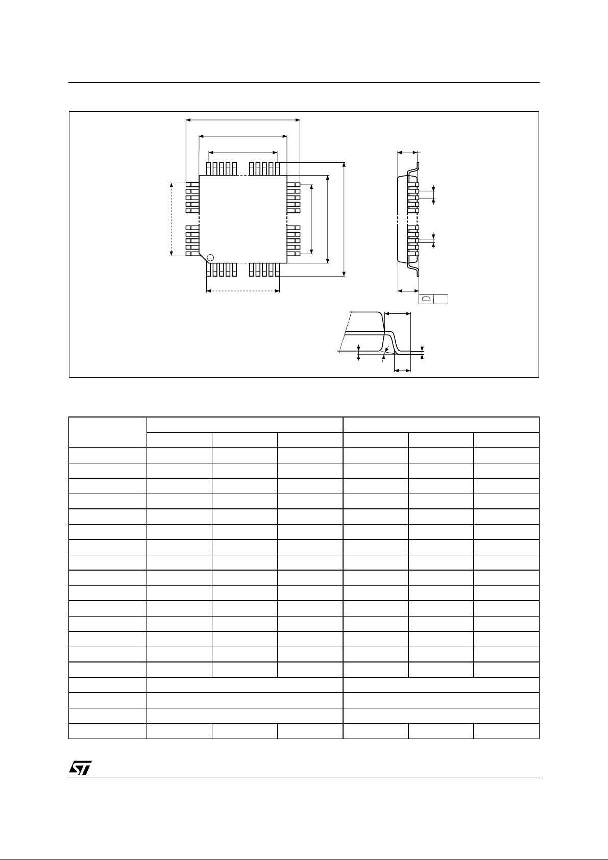
PQFP52 - 52 lead Plastic Quad Flatpack
D
D1
D2
DSM2180F3
A2
e
Ne
N
1
Nd
QFP
Note: Drawing is not to scale.
PQFP52 - 52 lead Plastic Quad Flatpack
Symb.
Typ. Min. Max. Typ. Min. Max.
A 2.35 0.093
A1 0.25 0.010
A2 2.00 1.80 2.10 0.079 0.077 0.083
b 0.22 0.38 0.009 0.015
c 0.11 0.23 0.004 0.009
D 13.20 12.95 13.45 0.520 0.510 0.530
D1 10.00 9.90 10.10 0.394 0.390 0.398
D2 7.80 – – 0.307 – –
E 13.20 12.95 13.45 0.520 0.510 0.530
E1 10.00 9.90 10.10 0.394 0.390 0.398
E2 7.80 – – 0.307 – –
e 0.65 – – 0.026
L 0.88 0.73 1.03 0.035 0.029 0.041
L1 1.60 – – 0.063
α
N52 52
Nd 13 13
Ne 13 13
CP 0.10 0.004
mm inches
0° 7° 0° 7°
E2
E1
E
b
A
L1
LA1 α
CP
c
59/63

DSM2180F3
Table 37. Pin Assignments – PQFP52
Pin No. Pin Assignments Pin No. Pin Assignments
1 PD2 27 AD4
2 PD1 28 AD5
3 PD0 29 AD6
4 PC7 30 AD7
5PC6 31
6 PC5 32 AD8
7 PC4 33 AD9
8
9 GND 35 AD11
10 PC3 36 AD12
11 PC2 37 AD13
12 PC1 38 AD14
13 PC0 39 AD15
14 PA7 40 CNTL0
15 PA6 41 RESET
16 PA5 42 CNTL2
17 PA4 43 CNTL1
18 PA3 44 PB7
19 GND 45 PB6
20 PA2 46 GND
21 PA1 47 PB5
22 PA0 48 PB4
23 AD0 49 PB3
V
CC
34 AD10
V
CC
60/63
24 AD1 50 PB2
25 AD2 51 PB1
26 AD3 52 PB0

PART NUMBERING
Table 38. Ordering Information Scheme
Example: DSM21 80 F3 - 90 T 6
Device Type
DSM21 = DSP System Memory for ADSP-21XX Family
DSP Applicability
80 = Analog Devices ADSP-218X family
Memory Density
F3 = 1 Mbit x 8 (128K Bytes)
Operating Voltage (Vcc)
blank = 5V ±10%
1
V
= 3.3V ± 10%
Access Time
90 = 90 nsec
15 = 150 nsec
DSM2180F3
Package
K = 52-pin PLCC
T = 52-pin PQFP
Temperature Range
6 = –40 to 85
Note: 1. The 3.3V±10% devices are not cov ered by this data sheet, but by t he DSM2180F3V data sheet.
For a list of available options (speed, package,
etc.) or for further information on any aspect of this
o
C (Industrial)
device, please contact your nearest ST Sales O ffice.
61/63

DSM2180F3
REVISION HIST ORY
Table 39. Document Revision History
Date Rev. Description of Revision
20-Jun-2001 1.0 Document written
06-Nov-2001 1.1 Information on the 3.3V±10% range removed to a separate data sheet
17-Dec-2001 1.2 PQFP52 package mechanical data updated
62/63

DSM2180F3
Information furnished is believed to be accurate and reliable. However, STMicroelectronics assumes no responsibility for the consequences
of use of such information nor for any infringement of patents or other rights of third parties which may result from its use. No license is granted
by implic ation or oth erwise unde r any patent or patent r i ghts of STMi croelectroni cs. Speci fications me ntioned in this publication are subject
to change without notice. This publication supersedes and replaces all information previously supplied. STMicroelectronics products are not
authorized for use as crit i cal components in life support devices or sy st em s without express writt en approval of STM i croelectronics.
The ST logo is registered trademark of STMicroelectronics
All other names are th e property of th ei r respective owners
© 2001 STMicroelectronics - All Rights Reserved
STMicroel ectronics group of companies Australia - Brazil - Canada - China - Finland - France - Germany - Hong Kong -
India - Israel - Italy - Japan - Malaysia - Malta - Morocco - Singapore - Spain - Sweden - Switzerland - United Kingdom - United States.
www.st.com
63/63
 Loading...