


DSM (Digital Signal Processor System Memory)
for Analog Devices DSPs (3.3V Supply)
FEATURES SUMMARY
■ Glueless Connection to DSP
– Easily add memory, logic, and I/O to the
External Port of ADSP-218x, 219x, 2106x,
2116x, 2153x, and TS101 families of DSPs
from Analog Devices, Inc.
■ Dual Flash Memories
– Two independent Flash memory arrays for
storing DSP code and data
– Capable of read-while-write concurrent Flash
memory operation
– Device can be configured as 8-bit or 16-bit
– Built-in programmable address decodi ng
logic allows mapping individual sectors of
each Flash array to any address boundary
– Each Flash sector can be write protected
■ 512 KByte Main Flash memory
– Ample storage for boot loading DSP code/
data upon reset and subsequent code swaps
– Large capacity for storing tables and
constants or for data recording
■ 32 KByte Secondary Flash memory
– Smaller sector size ideal for storing
calibration and configuration constants.
Eliminate external serial EEPROM.
– Optionally bypass internal DSP boot ROM
during start-up and execute code directly
from Secondary Flash. Use for custom start-
up code and In-Application Programming
(IAP).
■ Up to 40 Mult ifunction I/O Pin s
– Increase total DSP system I/O capability
– I/O controlled by DSP software or PLD logic
■ General pur pose PLD
– Use for peripheral glue logic to keypads,
control panel, displays, LCDs, and other
devices
– Over 3,000 gates of PLD with 16 macro cells
DSM2150F5V
– Eliminate PLDs and external logic devices
– Create state machines, chip selects , simple
shifters and counters, clock dividers, delays
– Simple PSDsoft Express
software, free from
■ In-System Programming (ISP) with JTAG
– Program entire chip in 15-35 seconds with no
involvement of the DSP
– Optionally links with DSP JTAG debug port
– Eliminate need for sockets and pre-
programming of memory and logic devices
– ISP allows efficient manufacturing and
product testing supporting Just-In-Time
inventory
– Use low-cost FlashLINK
Available from
■ Content Security
www.st.com/psm
– Programmable Sec urity Bit blocks access of
device programmers and readers
■ Operating Range
: 3.3V ± 10%, Temp: –40°C to +85°C
–V
CC
■ Zero-Power Technology
– 50µA standby current typical
■ Flash Memory Speed, Endurance, Retention
– 120ns, 100K cycles, 15 year retention
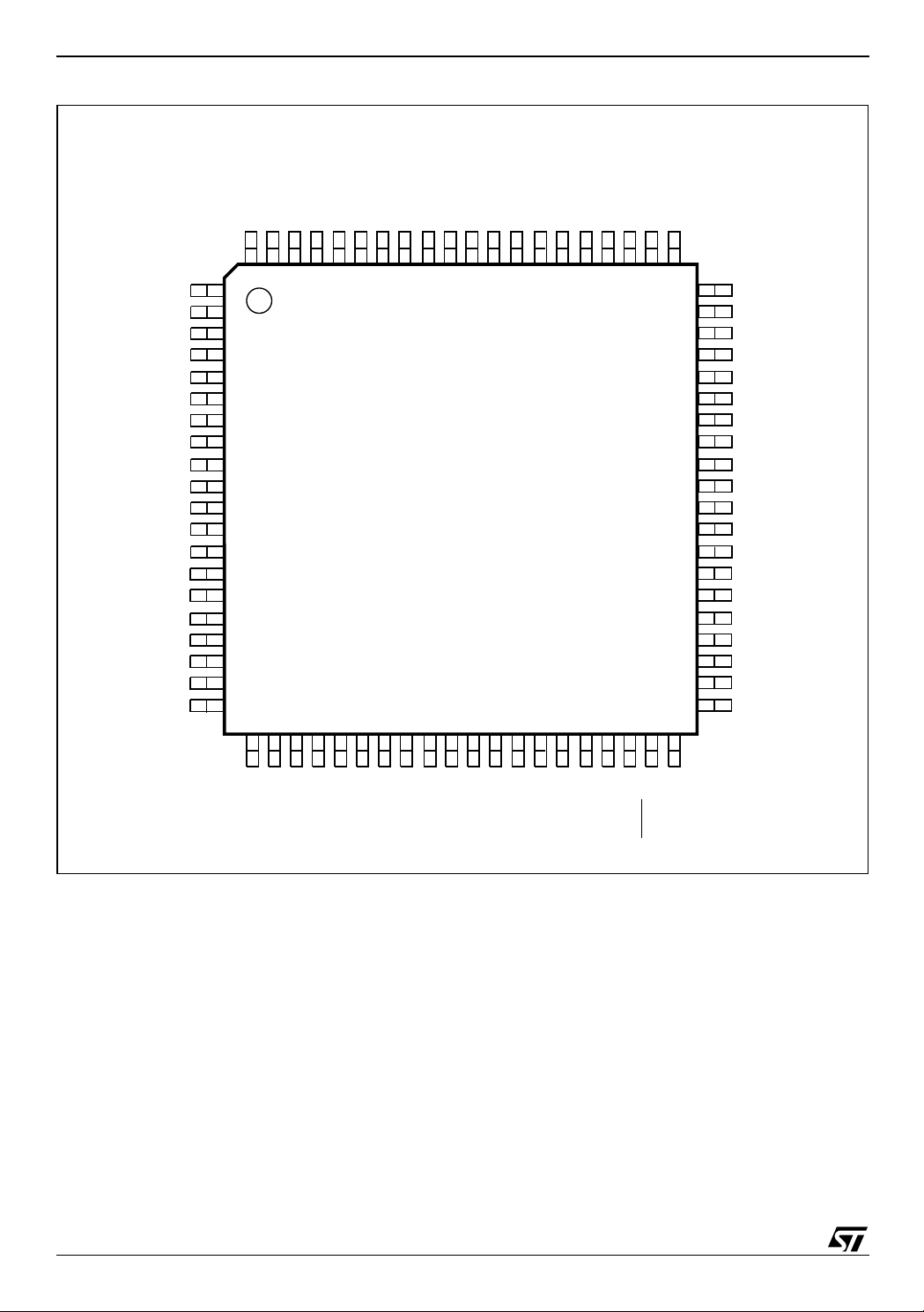
Figure 1. TQFP 80-pin Package
TQFP80 (T)
™
development
www.st.com/psm
™
cable with any PC.
.
Rev. 2.0
1/69March 2003

DSM2150F5V
TABLE OF CONTENTS
SUMMARY DESCRIPTION. . . . . . . . . . . . . . . . . . . . . . . . . . . . . . . . . . . . . . . . . . . . . . . . . . . . . . . . . . . 6
Figure 2. System Block Diagram, Two Chip Solution . . . . . . . . . . . . . . . . . . . . . . . . . . . . . . . . . . . . 6
Table 1. DSM2150F5V DSP Memory System Devices. . . . . . . . . . . . . . . . . . . . . . . . . . . . . . . . . . . 7
Table 2. Compatible Analog Devices DSPs . . . . . . . . . . . . . . . . . . . . . . . . . . . . . . . . . . . . . . . . . . . 7
Figure 3. TQFP Connections. . . . . . . . . . . . . . . . . . . . . . . . . . . . . . . . . . . . . . . . . . . . . . . . . . . . . . . 8
ARCHITECTURAL OVERVIEW . . . . . . . . . . . . . . . . . . . . . . . . . . . . . . . . . . . . . . . . . . . . . . . . . . . . . . . 9
DSP Address/Data/Control Interface . . . . . . . . . . . . . . . . . . . . . . . . . . . . . . . . . . . . . . . . . . . . . . . 9
Figure 4. Block Diagram . . . . . . . . . . . . . . . . . . . . . . . . . . . . . . . . . . . . . . . . . . . . . . . . . . . . . . . . . . 9
Main Flash Memory. . . . . . . . . . . . . . . . . . . . . . . . . . . . . . . . . . . . . . . . . . . . . . . . . . . . . . . . . . . . 10
Secondary Flash Memory. . . . . . . . . . . . . . . . . . . . . . . . . . . . . . . . . . . . . . . . . . . . . . . . . . . . . . . 10
Programmable Logic (PLDs) . . . . . . . . . . . . . . . . . . . . . . . . . . . . . . . . . . . . . . . . . . . . . . . . . . . .10
Runtime Control Registers. . . . . . . . . . . . . . . . . . . . . . . . . . . . . . . . . . . . . . . . . . . . . . . . . . . . . . 11
Memory Page Register . . . . . . . . . . . . . . . . . . . . . . . . . . . . . . . . . . . . . . . . . . . . . . . . . . . . . . . . . 11
I/O Ports . . . . . . . . . . . . . . . . . . . . . . . . . . . . . . . . . . . . . . . . . . . . . . . . . . . . . . . . . . . . . . . . . . . . . 11
JTAG ISP Port . . . . . . . . . . . . . . . . . . . . . . . . . . . . . . . . . . . . . . . . . . . . . . . . . . . . . . . . . . . . . . . . 11
Power Management . . . . . . . . . . . . . . . . . . . . . . . . . . . . . . . . . . . . . . . . . . . . . . . . . . . . . . . . . . . . 11
Security and NVM Sector Protection. . . . . . . . . . . . . . . . . . . . . . . . . . . . . . . . . . . . . . . . . . . . . . 11
Pin Assignments . . . . . . . . . . . . . . . . . . . . . . . . . . . . . . . . . . . . . . . . . . . . . . . . . . . . . . . . . . . . . . 11
Table 3. Pin Description (Pin Assignments in Appendix A). . . . . . . . . . . . . . . . . . . . . . . . . . . . . . . 12
RUNTIME CONTROL REGISTER DEFINITION. . . . . . . . . . . . . . . . . . . . . . . . . . . . . . . . . . . . . . . . . . 13
Table 4. CSIOP Registers and Their Offsets (in Hexadecimal). . . . . . . . . . . . . . . . . . . . . . . . . . . .13
DETAILED OPERATION. . . . . . . . . . . . . . . . . . . . . . . . . . . . . . . . . . . . . . . . . . . . . . . . . . . . . . . . . . . . 14
Flash Memories . . . . . . . . . . . . . . . . . . . . . . . . . . . . . . . . . . . . . . . . . . . . . . . . . . . . . . . . . . . . . . . 14
Table 5. Instruction Sequences for 8-bit Operation (Notes 1,2,3,4) . . . . . . . . . . . . . . . . . . . . . . . . 15
Table 6. Instruction Sequences for 16-bit Operation (Notes 1,2,3,4,15) . . . . . . . . . . . . . . . . . . . . . 17
Instruction Sequences . . . . . . . . . . . . . . . . . . . . . . . . . . . . . . . . . . . . . . . . . . . . . . . . . . . . . . . . . 19
Reading Flash Memory. . . . . . . . . . . . . . . . . . . . . . . . . . . . . . . . . . . . . . . . . . . . . . . . . . . . . . . . . 19
Table 7. Status Bit Definition. . . . . . . . . . . . . . . . . . . . . . . . . . . . . . . . . . . . . . . . . . . . . . . . . . . . . . 20
Programming Flash Memory . . . . . . . . . . . . . . . . . . . . . . . . . . . . . . . . . . . . . . . . . . . . . . . . . . . .21
Table 8. 16-Bit Data Bus with BHE . . . . . . . . . . . . . . . . . . . . . . . . . . . . . . . . . . . . . . . . . . . . . . . . . 21
Table 9. 16-Bit Data Bus with WRH and WRL . . . . . . . . . . . . . . . . . . . . . . . . . . . . . . . . . . . . . . . . 21
Figure 5. Data Polling Flowchart . . . . . . . . . . . . . . . . . . . . . . . . . . . . . . . . . . . . . . . . . . . . . . . . . . . 22
2/69

DSM2150F5V
PLDs . . . . . . . . . . . . . . . . . . . . . . . . . . . . . . . . . . . . . . . . . . . . . . . . . . . . . . . . . . . . . . . . . . . . . . . . 23
Table 10. DPLD and CPLD Inputs. . . . . . . . . . . . . . . . . . . . . . . . . . . . . . . . . . . . . . . . . . . . . . . . . .23
Figure 6. PLD Diagram . . . . . . . . . . . . . . . . . . . . . . . . . . . . . . . . . . . . . . . . . . . . . . . . . . . . . . . . . . 24
Decode PLD (DPLD) . . . . . . . . . . . . . . . . . . . . . . . . . . . . . . . . . . . . . . . . . . . . . . . . . . . . . . . . . . . 2 5
Figure 7. DPLD Logic Array. . . . . . . . . . . . . . . . . . . . . . . . . . . . . . . . . . . . . . . . . . . . . . . . . . . . . . . 25
Complex PLD (CPLD) . . . . . . . . . . . . . . . . . . . . . . . . . . . . . . . . . . . . . . . . . . . . . . . . . . . . . . . . . . 26
Figure 8. Macrocell and I/O Port . . . . . . . . . . . . . . . . . . . . . . . . . . . . . . . . . . . . . . . . . . . . . . . . . . . 26
Table 11. Output Macrocell Port and Data Bit Assignments . . . . . . . . . . . . . . . . . . . . . . . . . . . . . .27
Figure 9. CPLD Output Macrocell . . . . . . . . . . . . . . . . . . . . . . . . . . . . . . . . . . . . . . . . . . . . . . . . . . 29
Figure 10. Input Macrocell. . . . . . . . . . . . . . . . . . . . . . . . . . . . . . . . . . . . . . . . . . . . . . . . . . . . . . . . 30
DSP Bus Interface . . . . . . . . . . . . . . . . . . . . . . . . . . . . . . . . . . . . . . . . . . . . . . . . . . . . . . . . . . . . . 31
I/O Ports . . . . . . . . . . . . . . . . . . . . . . . . . . . . . . . . . . . . . . . . . . . . . . . . . . . . . . . . . . . . . . . . . . . . . 31
Figure 11. General Port Architecture. . . . . . . . . . . . . . . . . . . . . . . . . . . . . . . . . . . . . . . . . . . . . . . . 32
Port Operating Modes . . . . . . . . . . . . . . . . . . . . . . . . . . . . . . . . . . . . . . . . . . . . . . . . . . . . . . . . . . 32
Table 12. Port Operating Modes . . . . . . . . . . . . . . . . . . . . . . . . . . . . . . . . . . . . . . . . . . . . . . . . . . . 3 3
Ports A, B, and C – Functionality and Structure . . . . . . . . . . . . . . . . . . . . . . . . . . . . . . . . . . . . 34
Figure 12. Port A, B, and C Structure . . . . . . . . . . . . . . . . . . . . . . . . . . . . . . . . . . . . . . . . . . . . . . . 34
Port D – Functionality and Structure. . . . . . . . . . . . . . . . . . . . . . . . . . . . . . . . . . . . . . . . . . . . . . 35
Figure 13. Port D Structure . . . . . . . . . . . . . . . . . . . . . . . . . . . . . . . . . . . . . . . . . . . . . . . . . . . . . . . 35
Port E – Functionality and Structure. . . . . . . . . . . . . . . . . . . . . . . . . . . . . . . . . . . . . . . . . . . . . . 36
Port F – Functionality and Structure . . . . . . . . . . . . . . . . . . . . . . . . . . . . . . . . . . . . . . . . . . . . . . 36
Port G – Functionality and Structure. . . . . . . . . . . . . . . . . . . . . . . . . . . . . . . . . . . . . . . . . . . . . . 36
Figure 14. Port E and G Structure. . . . . . . . . . . . . . . . . . . . . . . . . . . . . . . . . . . . . . . . . . . . . . . . . . 3 6
POWER MANAGEMENT . . . . . . . . . . . . . . . . . . . . . . . . . . . . . . . . . . . . . . . . . . . . . . . . . . . . . . . . . . . 37
POWER-ON RESET, WARM RESET, AND POWER-DOWN . . . . . . . . . . . . . . . . . . . . . . . . . . . . . . . 38
Figure 15. Reset (RESET) Timing. . . . . . . . . . . . . . . . . . . . . . . . . . . . . . . . . . . . . . . . . . . . . . . . . . 38
Table 13. Status During Power-on Reset, Warm Reset and Power-down Mode . . . . . . . . . . . . . . 38
PROGRAMMING IN-CIRCUIT USING JTAG ISP. . . . . . . . . . . . . . . . . . . . . . . . . . . . . . . . . . . . . . . . . 39
Table 14. JTAG Port Signals. . . . . . . . . . . . . . . . . . . . . . . . . . . . . . . . . . . . . . . . . . . . . . . . . . . . . . 39
Initial Delivery State . . . . . . . . . . . . . . . . . . . . . . . . . . . . . . . . . . . . . . . . . . . . . . . . . . . . . . . . . . .40
AC AND DC PARAMETERS. . . . . . . . . . . . . . . . . . . . . . . . . . . . . . . . . . . . . . . . . . . . . . . . . . . . . . . . . 41
Figure 16. PLD ICC /Frequency Consumption (3.3V). . . . . . . . . . . . . . . . . . . . . . . . . . . . . . . . . . .41
MAXIMUM RATING. . . . . . . . . . . . . . . . . . . . . . . . . . . . . . . . . . . . . . . . . . . . . . . . . . . . . . . . . . . . . . . . 42
Table 15. Absolute Maximum Ratings . . . . . . . . . . . . . . . . . . . . . . . . . . . . . . . . . . . . . . . . . . . . . . . 42
3/69

DSM2150F5V
DC AND AC OPERATING AND MEASUREMENT CONDITIONS. . . . . . . . . . . . . . . . . . . . . . . . . . . . 43
Table 16. Operating Conditions . . . . . . . . . . . . . . . . . . . . . . . . . . . . . . . . . . . . . . . . . . . . . . . . . . . . 43
Table 17. AC Measurement Conditions. . . . . . . . . . . . . . . . . . . . . . . . . . . . . . . . . . . . . . . . . . . . . . 43
Figure 17. AC Measurement I/O Waveform . . . . . . . . . . . . . . . . . . . . . . . . . . . . . . . . . . . . . . . . . .43
Figure 18. AC Measurement Load Circuit. . . . . . . . . . . . . . . . . . . . . . . . . . . . . . . . . . . . . . . . . . . . 43
Table 18. Capacitance. . . . . . . . . . . . . . . . . . . . . . . . . . . . . . . . . . . . . . . . . . . . . . . . . . . . . . . . . . . 43
Figure 19. Switching Waveforms – Key. . . . . . . . . . . . . . . . . . . . . . . . . . . . . . . . . . . . . . . . . . . . . .44
Table 19. AC Symbols for PLD Timing . . . . . . . . . . . . . . . . . . . . . . . . . . . . . . . . . . . . . . . . . . . . . .44
Table 20. DC Characteristics. . . . . . . . . . . . . . . . . . . . . . . . . . . . . . . . . . . . . . . . . . . . . . . . . . . . . . 45
Table 21. CPLD Combinatorial Timing . . . . . . . . . . . . . . . . . . . . . . . . . . . . . . . . . . . . . . . . . . . . . .46
Table 22. CPLD MicroCell Synchronous Clock Mode Timing . . . . . . . . . . . . . . . . . . . . . . . . . . . . . 46
Table 23. CPLD MicroCell Asynchronous Clock Mode Timing . . . . . . . . . . . . . . . . . . . . . . . . . . . . 47
Figure 20. Input to Output Disable / Enable . . . . . . . . . . . . . . . . . . . . . . . . . . . . . . . . . . . . . . . . . . 47
Figure 21. Asynchronous Reset / Preset. . . . . . . . . . . . . . . . . . . . . . . . . . . . . . . . . . . . . . . . . . . . . 47
Figure 22. Synchronous Clock Mode Timing – PLD . . . . . . . . . . . . . . . . . . . . . . . . . . . . . . . . . . . . 48
Figure 23. Asynchronous Clock Mode Timing (Product Term Clock) . . . . . . . . . . . . . . . . . . . . . . . 48
Figure 24. Input MicroCell Timing (Product Term Clock) . . . . . . . . . . . . . . . . . . . . . . . . . . . . . . . . 49
Table 24. Input MicroCell Timing. . . . . . . . . . . . . . . . . . . . . . . . . . . . . . . . . . . . . . . . . . . . . . . . . . . 4 9
Figure 25. READ Timing . . . . . . . . . . . . . . . . . . . . . . . . . . . . . . . . . . . . . . . . . . . . . . . . . . . . . . . . . 50
Table 25. READ Timing. . . . . . . . . . . . . . . . . . . . . . . . . . . . . . . . . . . . . . . . . . . . . . . . . . . . . . . . . . 50
Figure 26. WRITE Timing . . . . . . . . . . . . . . . . . . . . . . . . . . . . . . . . . . . . . . . . . . . . . . . . . . . . . . . . 51
Table 26. WRITE Timing. . . . . . . . . . . . . . . . . . . . . . . . . . . . . . . . . . . . . . . . . . . . . . . . . . . . . . . . . 5 1
Table 27. Flash Memory Program, WRITE and Erase Times . . . . . . . . . . . . . . . . . . . . . . . . . . . . . 52
Figure 27. Reset (RESET) Timing. . . . . . . . . . . . . . . . . . . . . . . . . . . . . . . . . . . . . . . . . . . . . . . . . . 52
Table 28. Reset (RESET) Timing . . . . . . . . . . . . . . . . . . . . . . . . . . . . . . . . . . . . . . . . . . . . . . . . . . 52
Figure 28. ISC Timing . . . . . . . . . . . . . . . . . . . . . . . . . . . . . . . . . . . . . . . . . . . . . . . . . . . . . . . . . . . 53
Table 29. ISC Timing. . . . . . . . . . . . . . . . . . . . . . . . . . . . . . . . . . . . . . . . . . . . . . . . . . . . . . . . . . . . 53
PACKAGE MECHANICAL . . . . . . . . . . . . . . . . . . . . . . . . . . . . . . . . . . . . . . . . . . . . . . . . . . . . . . . . . . 54
PART NUMBERING . . . . . . . . . . . . . . . . . . . . . . . . . . . . . . . . . . . . . . . . . . . . . . . . . . . . . . . . . . . . . . . 56
APPENDIX A. TQFP80 PIN ASSIGNMENTS. . . . . . . . . . . . . . . . . . . . . . . . . . . . . . . . . . . . . . . . . . . . 57
4/69

DSM2150F5V
APPENDIX B. CSIOP REGISTER BIT DEFINITIONS . . . . . . . . . . . . . . . . . . . . . . . . . . . . . . . . . . . . . 58
Table 33. Data-In Registers – Ports A, B, C, D, E, G . . . . . . . . . . . . . . . . . . . . . . . . . . . . . . . . . . . 58
Table 34. Data-Out Registers – Ports A, B, C, D, E, G. . . . . . . . . . . . . . . . . . . . . . . . . . . . . . . . . . 58
Table 35. Direction Registers – Ports A, B, C, D, E, G . . . . . . . . . . . . . . . . . . . . . . . . . . . . . . . . . . 58
Table 36. Drive Registers – Ports A, B, E, G. . . . . . . . . . . . . . . . . . . . . . . . . . . . . . . . . . . . . . . . . . 58
Table 37. Drive Registers – Port C . . . . . . . . . . . . . . . . . . . . . . . . . . . . . . . . . . . . . . . . . . . . . . . . . 5 8
Table 38. Enable-Out Registers – Ports A, B, C . . . . . . . . . . . . . . . . . . . . . . . . . . . . . . . . . . . . . . . 58
Table 39. Input Macrocells – Ports A, B, C . . . . . . . . . . . . . . . . . . . . . . . . . . . . . . . . . . . . . . . . . . .58
Table 40. Output Macrocells A Register . . . . . . . . . . . . . . . . . . . . . . . . . . . . . . . . . . . . . . . . . . . . .59
Table 41. Output Macrocells B Register . . . . . . . . . . . . . . . . . . . . . . . . . . . . . . . . . . . . . . . . . . . . .59
Table 42. Mask Macrocells A Register . . . . . . . . . . . . . . . . . . . . . . . . . . . . . . . . . . . . . . . . . . . . . .59
Table 43. Mask Macrocells B Register . . . . . . . . . . . . . . . . . . . . . . . . . . . . . . . . . . . . . . . . . . . . . .59
Table 44. Flash Memory Protection Register . . . . . . . . . . . . . . . . . . . . . . . . . . . . . . . . . . . . . . . . . 59
Table 45. Flash Boot Protection Register . . . . . . . . . . . . . . . . . . . . . . . . . . . . . . . . . . . . . . . . . . . .59
Table 46. JTAG Enable Register . . . . . . . . . . . . . . . . . . . . . . . . . . . . . . . . . . . . . . . . . . . . . . . . . . . 59
Table 47. Page Register . . . . . . . . . . . . . . . . . . . . . . . . . . . . . . . . . . . . . . . . . . . . . . . . . . . . . . . . . 60
Table 48. PMMR0 Register. . . . . . . . . . . . . . . . . . . . . . . . . . . . . . . . . . . . . . . . . . . . . . . . . . . . . . . 6 0
Table 49. PMMR2 Register. . . . . . . . . . . . . . . . . . . . . . . . . . . . . . . . . . . . . . . . . . . . . . . . . . . . . . . 6 0
Table 50. Memory_ID0 Register . . . . . . . . . . . . . . . . . . . . . . . . . . . . . . . . . . . . . . . . . . . . . . . . . . . 60
Table 51. Memory_ID1 Register . . . . . . . . . . . . . . . . . . . . . . . . . . . . . . . . . . . . . . . . . . . . . . . . . . . 60
APPENDIX C. TYPICAL CONNECTIONS, DSM2150F5V AND ADSP-21535 BLACKFIN DSP. . . . . 61
Figure 30. Typical Connections, DSM2150F5V and ADSP-21535 Blackfin DSP . . . . . . . . . . . . . . 61
Typical Memory Map, DSM2150F5V and ADSP21535 BL ACKFIN DSP. . . . . . . . . . . . . . . . . . . 62
Figure 31. Memory Map, ADSP-21535 . . . . . . . . . . . . . . . . . . . . . . . . . . . . . . . . . . . . . . . . . . . . . . 62
Specifying the Memory Map with PSDsoft Express™. . . . . . . . . . . . . . . . . . . . . . . . . . . . . . . . 63
Table 52. HDL Statements Generated from PSDsoft Express to Implement Memory Map . . . . . . 63
Figure 32. PSDsoft Express™ Memory Mapping . . . . . . . . . . . . . . . . . . . . . . . . . . . . . . . . . . . . . . 63
APPENDIX D. TYPICAL CONNECTIONS, DSM2150F5V AND ADSP-21062 SHARC DSP . . . . . . . 64
Figure 33. Typical Connections, DSM2150F5V and ADSP-21062 Sharc DSP. . . . . . . . . . . . . . . . 64
APPENDIX E. TYPICAL CONNECTIONS, DSM2150F5V AND ADSP-TS101S TIGERSHARC DSP. 65
Figu r e 3 4 . Typical C o n nectio ns, ADSP-TS101 S TigerSHAR C DS P . . . . . . . . . . . . . . . . . . . . . . . . 65
APPENDIX F. TYPICAL CONNECTIONS, DSM2150F5V AND ADSP-2191. . . . . . . . . . . . . . . . . . . . 66
Figure 35. Typical Connections, DSM2150F5V and ADSP-2191M . . . . . . . . . . . . . . . . . . . . . . . . 66
APPENDIX G. TYPICAL CONNECTIONS, DSM2150F5V AND ADSP-2188M . . . . . . . . . . . . . . . . . . 67
Figure 36. Typical Connections, DSM2150F5V and ADSP-2188M . . . . . . . . . . . . . . . . . . . . . . . . 67
REVISION HISTORY . . . . . . . . . . . . . . . . . . . . . . . . . . . . . . . . . . . . . . . . . . . . . . . . . . . . . . . . . . . . . . . 68
5/69

DSM2150F5V
SUMMARY DESCRIPTION
The DSM2150F5V is an 8 or 16-bit system memory device for use with the Analog Devices DSPs.
DSM means Digital signal processor System
Memory. A DSM device brings In-System Programmable (ISP) Flash memory, param eter storage, programmable logic, and additional I/O to
DSP systems. The result is a flexible two-chip solution for DSP designs. On-chip integrated memory decode logic makes it easy to map dual banks
of Flash memory to the DSP s in a vari ety of ways
for bootloading or bypassing DSP boot ROM, code
execution, data recording, code swapping, and
parameter storage.
JTAG ISP reduces development time, simplifies
manufacturing flow, and lowers the cost of field upgrades. The JTAG ISP interface eliminates the
need for sockets and pre-programmed memory
and logic devices. End products may be manufactured with a blank DSM device soldered down and
programmed at the end of the assembly line in 15
to 35 seconds with no involvement of the DSP.
Rapidly program test code, then application code
as determined by Just-In Time inventory requirements. Additionally, JTAG ISP reduce s development time by turning fast iterations of DSP code in
the lab. Code updates in the field require no product disassembly. The FlashLINK
ming cable costs $59 USD and plugs into any PC
parallel port. Programming through conventional
device insertion programmers is also available using PSDpro from STMicroelectronics and other 3rd
party programmers. See
www.st.com/psm
™
JTAG program-
.
DSM devices add programmable logic (PLD) and
up to 32 configurable I/O pins to the DSP system.
The state of I/O pins can be driven by DSP software or PLD logic. PLD and I/O conf iguration are
programmable by JTAG ISP. The PLD consists of
more than 3000 gates and has 16 macro cell registers. Common uses for the PLD include chip-selects for external devices, state-machines, simple
shiftier and counters, keypad and control panel interfaces, clock dividers, handshake delay, muxes,
etc., eliminating the need for small external PLDs
and logic devices. Configuration of PLD, I/O, and
Flash memory mapping is easily entered in a
point-and-click environment using the software
development tool, PSDsoft Express
no charge from
www.st.com/psm
™
, available at
. The two-chip
DSP/DSM combination is ideal for systems having
limitations on size, EMI levels, and power consumption. DSM memory and logic are “zero-power”, meaning they automatically go to standby
between memory accesses or logic input changes, producing low active and standby current consumption, which is ideal for battery powered
products.
A programmable security bit in the DSM protects
its contents from unauthorized viewing and copying. When set, the security bit will block access of
programming devices (JTAG or others) to the
DSM Flash memories and PLD configuration. The
only way to defeat the security bit is to erase the
entire DSM device, after which the device is blank
and may be used again. The DSP will always have
access to Flash memory contents through the data
bus, even with security bit set.
Figure 2. System Block Diagram, Two Chip Solution
DSM2150F5V
DSP SYSTEM MEMORY
I/O FLAGS
SERIAL
DEVICE
SERIAL
DEVICE
SDRAM
HOST
MCU
6/69
ANALOG
DEVICES
DSP
ADSP-218x
ADSP-219x
ADSP-2153x
ADSP-2106x
ADSP-2116x
ADSP-TS101S
JTAG DEBUG (All But ADSP-218x Family)
ADDRESS
CONTROL
8 or 16 DATA
FLASH MEMORY
LOGIC
FLASH MEMORY
ADDR& DECODE
16 MACROCELL PLD
I/O CONTROL
POWER MANAGEMENT
CONTENT SECURITY
PRIMARY
512 Kbytes
SECONDARY
32 Kbytes
I/O BUS
16 I/O
PORTS
I/O, PLD, CHIP SELECTS
WITH
PLD
8 to 16
I/O
GENERAL PURPOSE I/O
PORTS
JTAG
ISP TO
ALL
AREAS
JTAG ISP
AI05732

Table 1. DSM2150F5V DSP Memory System Devices
Part Number
Main Flash
Memory
Secondary
Flash Mem
PLD
I/O
Ports
V
CC
and I/O
Mem
Speed
DSM2150F5V
Package Op Temp
DSM2150F5V-12T6
512 KBytes,
eight 64-KByte
sectors
32 KBytes,
four 8-KByte
sectors
16
macro
cells
Up to
40
3.3V ±10% 120ns
80-pin
TQFP
Table 2. Compatible Analog Devices DSPs
DSP Part Number Core Operating Voltage I/O Voltage
ADSP-2183, 2184L, 2185L, 2186L, 2187L 3.3V 3.3V
ADSP-2185M, 2186M, 2188M, 2189M 2.5V 3.3V
ADSP-2184N, 2185N, 2186N, 2187N, 2188N, 2189N 1.8V 3.3V
ADSP-2191M, 2195M, 2196M 2.5V 3.3V
Blackfin ADSP-215 32S 3.3V 3.3V
Blackfin ADSP-215 35P 1.5V 3.3V
Sharc ADSP-21060L, 21061L, 21062L, 21065L 3.3V 3.3V
Sharc ADSP-21160M 2.5V 3.3V
Sharc ADSP-21160N, 21161N 1.8V 3.3V
Tiger Sharc ADSP-TS101S 1.0V 3.3V
–40
+85
o
C to
o
C
7/69
DSM2150F5V
Figure 3. TQ FP Connection s
PD1
PD0
80797877767574737271706968676665646362
PE7
PE6
PE5
PE4
PE3
PE2
PE1
PE0
GND
VCCPB7
PB6
PB5
PB4
PB3
PB2
PB1
PB0
61
PD2
PD3
AD0
AD1
AD2
AD3
AD4
GND
V
CC
AD5
AD6
AD7
AD8
AD9
AD10
AD11
AD12
AD13
AD14
AD15
1
2
3
4
5
6
7
8
9
10
11
12
13
14
15
16
17
18
19
20
21222324252627282930313233343536373839
CC
PF0
PF1
PF2
PF3
PF4
PF5
PF6
PG0
PG1
PG2
PG3
PG4
PG5
PG6
PG7
V
GND
PF7
RESET
40
CNTL2
60 CNTL1
59 CNTL0
58 PA7
57 PA6
56 PA5
55 PA4
54 PA3
53 PA2
52 PA1
51 PA0
50 GND
49 GND
48 PC7
47 PC6
46 PC5
45 PC4
44 PC3
43 PC2
42 PC1
41 PC0
AI04943
8/69

ARCHITECTURAL OVERVIEW
Major functional blocks are shown in Figure 4.
DSP Address/Data/Control Interface
These DSP signals attach directly to the DSM for
a glueless connection. An 8-bit or 16-bit data connection is formed and 16 or more DSP address
lines can be decoded as well as various DSP
memory strobes; i.e.
BMS, RD, AWE, IOMS, MSx,
etc. The data path width must be specified as 8bits or 16-bits in PSDsoft Express. This configura-
Figure 4. Block Diagram
DSM2150F5V
tion is a static, meaning the data path width cannot
switch between 8-bits and 16-bits during runtime.
Port F is used for 8-bit data path, Ports F and G are
used for 16-bit data path. There are many different
ways the DSM2150F5V can be configured and
used depending on system requirements. See Appendices for example connections between the
DSM2150F5V and different DSPs.
DSP ADDR
AD0
AD1
AD2
AD3
AD4
AD5
AD6
AD7
AD8
AD9
AD10
AD11
AD12
AD13
AD14
AD15
DSP DATA
PF0
PF1
PF2
PF3
PF4
PF5
PF6
PF7
DSP DATA
or GP I/O
PG0
PG1
PG2
PG3
PG4
PG5
PG6
PG7
DSP CNTL
CNTL0
CNTL1
CNTL2
RST\
INTERNAL ADDR, DATA, CONTROL BUS LINKED TO DSP
SECURITY
LOCK
PAGE REG
DECODE
PLD
GENERAL PLD
PLD INPUT BUS
PIN FEEDBACK
NODE FEEDBACK
INTERNAL ADDR, DATA, CONTROL BUS LINKED TO DSP
AND
ARRAY
AAAAAAAA
BBBBBBBBCCCCCCCC
FS0-7
CSBOOT0-3
CSIOP
ECS0-7
AAAAAA
AA
BBBBBBBB
16 OUTPUT MICROCELLS
24 INPUT
MICROCELLS
DSM2150F5V
DSP System Memory
MAIN FLASH
8 BLOCKS, 64 KB
512 KBytes total
SECONDARY FLASH
4 BLOCKS, 8 KB
32 KBytes total
RUNTIME CONTROL
GPIO
PLD
POWER MNGMT
JTAG ISP
CONTROLLER
TO PLD
IN BUS
I/O PORT
PD0
PD1
PD2
PD3
I/O PORT
PA0
PA1
PA2
PA3
PA4
PA5
PA6
PA7
I/O PORT
PB0
PB1
PB2
PB3
PB4
PB5
PB6
PB7
I/O PORT
PC0
PC1
PC2
PC3
PC4
PC5
PC6
PC7
I/O PORT
PC0
PC1
PC2
PC3
PC4
PC5
PC6
PC7
AI05776
9/69

DSM2150F5V
Main Flash Memory
The 4M bit (512 KByte) Main Flash memory is divided into eight equally-sized 64 KByte sectors
that are individually selectable through the Decode PLD. Each Flash memory s ector can be located at any address as defined by the user with
PSDsoft Express. DSP code and data are easily
placed in flash memory using PSDsoft Express,
the software development tool.
Secondary Flash Memory
The 256Kbit (32 KByte) Secondary Flash memory
is divided into eight equally-sized 8 KByt e sec tors
that are individually selectable through the Decode PLD. Each Flash memory s ector can be located at any address as defined by the user with
PSDsoft Express. DSP code and data can also be
placed Secondary Flash memory using the PSDsoft Express development tool.
Secondary flash memory is good for storing dat a
because of its smaller sectors. Software EEPROM
emulation techniques can be used for small data
sets that change frequently on a byte-by-byte basis.
Secondary flash may also be used to store custom
start-up code for applications that do not “boot” using DMA, but instead start executing code from external memory upon reset (bypass internal DSP
boot ROM). Storing code here can keep the entire
Main Flash free of initialization code for clean software partitioning. If only one or more 8 KByte sectors are needed for start-up code, the remaining
sectors of Secondary Flash may be used for data
storage.
In-Application-Programming (IAP) may be implemented using Secondary Flash. For example,
code to implement IAP over a USB channel may
be stored here. The DSP executes code from Secondary Flash array while erasin g and writing new
code to the Main Flash array as it is received over
the USB channel. Any communication channel
that the DSP supports can be used for IAP.
Secondary Flash may also be used as an extension to Main Flash memory producing a total of
544 KBytes.
Miscellaneous: Main and Secondary Flash memories are totally independent, allowing concurrent
operation. The DSP can read from one memory
while erasing or programming the other. The DSP
can erase Flash memories by individual sectors or
the entire Flash memory array may be erased at
one time. Each sector in either Flas h memory array may be individually write protected, bloc king
any WRITEs from the DSP (good for boot and
start-up code protection). The Flash memories automatically go to standby between DSP READ or
WRITE accesses to conserve power. Maximum
access times include sector decoding time. Maxi-
mum erase cycles is 100K and data retention is 15
years minimum. Flash memory, as well as the entire DSM device may be programmed with the
JTAG ISP interface with no DSP involvement.
Programm a b le Logic (PLDs)
The DSM family contains two PLDS that m ay optionally run in Turbo or Non-Turbo Mode. PLDs operate faster (less propagation delay) while in
Turbo Mode but consume more power than NonTurbo Mode. Non-Turbo Mode allows the PLDs to
automatically go to standby when no inputs are
change to conserve power. The Turbo Mode setting is controlled at runtime by DSP software.
Decode PLD (DPLD). This is programmable logic used to select one of the eigh t individual Main
Flash memory segments, one of four individual
Secondary Flash memory segments, or the group
of control registers within the DSM device. The
DPLD can also drive ex ternal chip select signals
on Port C pins. DPLD input signals include: DSP
address and control signals, Page Register outputs, DSM Port Pins, CPLD logic feedback.
Complex PLD (CPLD). This programmab le logic
is used to c reate bo th combinatorial and sequential general purpose logic. The C PLD contains 16
Output Macrocells (OMCs) and 24 Input Macrocells (IMCs). PSD Macroc ell registers are unique
in that they have direct connection to the DSP data
bus allowing them to be loaded and read directly
by the DSP at runtime. This di rect access is g ood
for making small peripheral devices (shiftier,
counters, state machines, etc.) that are accessed
directly by the DSP with little overhead. DPLD inputs include DSP address and control signals,
Page Register outputs, DSM Port Pins, and CPLD
feedback.
OMCs: The general structure of the CPLD is similar in nature to a 22V10 PLD device wit h t he familiar sum-of-products (AND-OR) construct. True
and compliment versions of 73 input signals are
available to a large AND array. AND array outputs
feed into a multiple product-term O R gate within
each OMC (up to 10 product-terms for each
OMC). Logic output of the OR gate can be passed
on as combinatorial logic or combined with a flipflop within in each OMC to realize sequential logic.
OMCs can be used a s a buried nodes with feedback to the AND array or OMC output can be routed to pins on Port A or Port B.
IMCs: Inputs from pins on Ports A, B or C are routed to IMCs for condi tioning (clocking or latching)
as they enter the chip, which is good for sampl ing
and debouncing inputs. Alternatively, IMCs can
pass Port input signals directly to PLD inputs without clocking or latching. Th e DSP may read the
IMCs at any time.
10/69

Runtime Control Registers
A block of 256 byt es is decoded inside the DSM
device for control and status registers. 50 registers
are used from the block of 256 locations to control
the output state of I/O pins, to READ I/O pins, to
control power management, to READ/WRITE
macrocells, and other functions at runtime. See
Table 4 for description. The base address of these
256 locations is referred to in this data sheet as
csiop
(Chip Select I/O Port). Individual registers
within this block are accessed with an offset from
the base address. Some DSPs can ac cess
csiop
registers using I/O memory with the IOMS strobe (if
csiop
equipped).
registers are bytes. When the
DSM is configured for 16-bit operation, csiop registers are read in byte pairs at even addresses
only. Care should be taken while writing
csiop
registers to ensure the proper byte is written within the
byte pair. This is not a problem for DSPs that support the BHE
CNTL2 input pin, or WRL
(Byte High Enable) signal on the
, WRH (WRITE low byte,
WRITE high byte) on the CNTL0 and PD3 input
pins of the DSM2150F5V.
Memory Page Register
This 8-bit register can be l oaded and read b y the
csiop
DSP at runtime as one of the
registers. Its
outputs feed directly into both PLDs. The page
register can be used for special m emo ry mappi ng
requirements and also for general logic.
I/O Po r t s
The DSM has 52 individually configurable I/O pins
distributed over the seven ports (Ports A, B, C, D,
E, F, and G). At least 32 I/O are available when
DSM2150F5V is connected with 8-bit data path,
and at least 24 I/O are available with 16-bit data
path. Each I/O pin can be indiv idually configured
for different functions such as standard MCU I/O
ports or PLD I/O on a pin by pin basis. (MCU I/O
means that for each pin, its output state can be
controlled or its input value can be read by the
csiop
DSP at runtime using the
registers like an
MCU would do.)
The static configuration of all Port pins is d efined
with the PSDsoft Express
™
software development
tool. The dynamic action of the Ports pins is controlled by DSP runtime software.
JTAG ISP Port
In-System Programming (ISP) can be pe rformed
through the JTAG signals on Port E. This serial interface allows programming of the entire DSM device or subsections (that is, only Flash memory, for
example) without the participation of the DSP. A
blank DSM device soldered to a circuit board can
be completely programmed in 15 to 35 seconds.
The basic JTAG signals; TMS, TCK, TDI, and
TDO form the IEEE-1149.1 interface. The DSM
DSM2150F5V
device does not implement the IEEE-1149.1
Boundary Scan functions. The DSM uses the
JTAG interface for ISP only. However, the DSM
device can reside i n a standard JTAG chain with
other JTAG devices and it will remain in BYPASS
Mode while other devices perform Boundary
Scan.
ISP programming time can be reduced as much as
30% by using two more signals on Port E, TSTAT
and TERR
The FlashLINK
available from STMicroelectronics for $USD59
and PSDsoft Express software is available at no
charge from
needed to program a DSM device using the parallel port on any PC or notebook. See sec tion titled
“PROGRAMMING IN-CIRCUIT USING JTAG
ISP” on page 39.
Power Management
The DSM has bits in
figured at run-time by the DSP to reduc e power
consumption of the CPLD. The Turbo Bit in the
PMMR0 register can be set to logic '1' and the
CPLD will go to Non-Turbo Mode, meaning it will
latch its outputs and go to sleep until the next transition on its inputs. There is a slight penalty in PLD
performance (longer propagation delay), but significant power savings are realized.
Additionally, other bits in two
be set by the DSP to selectively block signals from
entering the CPLD which reduces power consumption.
Both Flash memories automatically go to standby
current between accesses. No user action required.
Security and NVM Sector Protection
A programmable security bit in the DSM protects
its contents from unauthorized viewing and copying. When set, the security bit will block access of
programming devices (JTAG or others) to the
DSM Flash memory and PLD configuration. The
only way to defeat the security bit is to erase the
entire DSM device, after which the device is blank
and may be used again.
Additionally, the content s of ea ch in dividual F lash
memory sector can be write protected (sector protection) by configuration with PSDsoft Express
This is typically used to protect DSP boot code
from being corrupted by inadvertent WRITEs to
Flash memory from the DSP.
Pin Assign m ent s
Pin assignment are shown for the 80-pin TQFP
package in Figure 3, page 8, and their description
in Table 3, page 12.
in addition to TMS, TCK, TDI and TDO.
™
JTAG programming cable is
www.st.com/psm
csio p
. That is all that is
registers that are con-
csio p
registers can
™
.
11/69
DSM2150F5V
Table 3. Pin Description (Pin Assignments in Appendix A)
Pin Name Type Description
AD0-15 In Sixteen address inputs from the DSP.
CNTL0 In
CNTL1 In Active low READ strobe input from the DSP.
CNTL2 In
Active low WRITE strobe input from the DSP, typically connected to DSP WR
functions as WRL
Programmable control input. CNTL2 may be used for BHE
DSM2150F5V is configured for 16-bit operation. BHE = ’0’ will allow a byte WRITE from data lines
D8-D15 ignoring data lines D0-D7. BHE
lines D8-D15. DSP READ operations are not affected by BHE
for DSPs which use WRL strobe when writing low byte only in 16-bit word.
= 1 will allow a byte WRITE from D0-D7 ignoring data
signal. Also
(Byte High Enable) when
(always read both bytes).
Reset In
PA0-7 I/O
PB0-7 I/O
PC0-7 I/O
PD0-3 I/O
PE0-7 I/O
Active low reset input from system. Resets DSM I/O Ports, Page Register contents, and other
DSM configuration registers. Must be logic Low at Power-up.
Eight configurable Port A signals with the following functions:
1. MCU I/O – DSP may write or read pins directly at runtime with csiop registers.
2. CPLD Output Macrocell (McellA0-7) outputs.
3. Inputs to the PLDs (via Input Macrocells). Can be used to input address A16 and above.
Note: PA0-PA7 may be configured at run-time as standard CMOS or Open Drain Outputs.
Eight configurable Port B signals with the following functions:
1. MCU I/O – DSP may write or read pins directly at runtime with csiop registers.
2. CPLD Output Macrocell (McellB0-7 or McellC0-7) outputs.
3. Inputs to the PLDs (via Input Macrocells). Can be used to input address A16 and above.
Note: PB0-PB7 may be configured at run-time as standard CMOS or Open Drain Outputs.
Eight configurable Port C signals with the following functions:
1. MCU I/O – DSP may write or read pins directly at runtime with csiop registers.
2. DPLD chip-select outputs (ECS0-7, does not consume MicroCells).
3. Inputs to the PLDs (via Input Macrocells). Can be used to input address A16 and above.
Note: PC0-PC7 may be configured at run-time as standard CMOS or Faster Slew Rate Output.
Four configurable Port D signals with the following functions:
1. MCU I/O – DSP may write or read pins directly at runtime with csiop registers.
2. Input to the PLDs (no associated Input Macrocells, routes directly into PLDs). Can be used to
input address A16 and above.
3. PD1 can be configured as CLKIN, a common clock input to PLD.
4. PD2 can be configured as CSI
memory is disabled to conserve more power when CSI
5. PD3 can be used for WRH
Eight configurable Port E signals with the following functions:
1. MCU I/O – DSP may write or read pins directly at runtime with csiop registers.
2. PE0, PE1, PE2, and PE3 can form the JTAG IEEE-1149.1 ISP serial interface as signals TMS,
TCK, TDI, and TDO respectively.
3. PE4 and PE5 can form the enhanced JTAG signals TSTAT and TERR
ISP programming time up to 30% when used in addition to the standard four JTAG signals: TDI,
TDO, TMS, TCK.
4. PE4 can be configured as the Ready/Busy output to indicate Flash memory programming status
during parallel programming. May be polled by DSP or used as DSP interrupt.
Note 1: PE0-PE7 may be configured at run-time as either standard CMOS or Open Drain Outputs.
Note 2: The JTAG ISP pins may be multiplexed with other I/O functions.
, active low Chip Select Input to select Flash memory. Flash
is logic high.
strobe from DSP to write high byte only for 16-bit configuration.
respectively. Reduces
PF0-7 I/O Port F connects to eight data bus signals, D0 - D7 from DSP.
Port G connects to eight data bus signals, D8 - D15 from DSP if 16-bit data path is used.
PG0-7 I/O
V
CC
GND Ground pins
12/69
Otherwise, PG0-PG7 can be used for general purpose MCU I/O pins.
Note: PG0-PG7 may be configured at run-time as standard CMOS or Open Drain Outputs.
Supply Voltage

RUNTIME CONTROL REGISTER DEFINITION
A block of 256 addresses are decoded inside the
DSM2150F5V for control and status. 50 locations
contain registers that the DSP a ccesses at runtime. The base address of the registers is called
csio p
(Chip Select I/O Po rt). T able 4 lists the reg-
DSM2150F5V
isters and their offsets (in hex adecimal) from the
csio p
base. See Appendix B for bit definitions.
Note: Do not write to unused locations, they
should remain logic zero.
Note: See Table 13, page 38 for register state at
reset and at power-on.
Table 4.
Data In 00 01 10 11 30 41
Data Out 04 05 14 15 34 45
Direction 06 07 16 17 36 47
Drive Select 08 09 18 19 38 49
Input
Macrocells
Enable Out 0C 0D 1C
Output
Macrocells A
Output
Macrocells B
Mask
Macrocells A
Mask
Macrocells B
Main Flash
Sector Protect
Security Bit
and Secondary
Flash Sector
Protection
JTAG Enable C7
PMMR0 B0 Power Management Register 0. WRITE and READ.
PMMR2 B4 Power Management Register 2. WRITE and READ.
Page E0 Memory Page Register. WRITE and READ.
Memory_ID0 F0 Read to get size of Main Flash memory. No WRITEs.
Memory_ID1 F1 Read to get size of 2nd Flash memory. No WRITEs.
CSIOP
Register
Name
Registers and Their Offsets (in Hexadecimal)
Por
Por
Por
Por
Por
Por
t A
t B
t C
t D
t E
0A 0B 1A Read to obtain state of IMCs. No WRITEs.
20
23
Other Description
t G
MCUI/O Input Mode. Read to obtain current logic
level of Port pins. No WRITEs.
MCU I/O Output Mode. Write to set logic level on
Port pins. Read to check status.
MCU I/O Mode. Configures Port pin as input or
output. Write to set direction of Port pins.
Logic ’1’ = out, Logic ’0’ = in. Read to check status.
Write to configure Port pins as either standard
CMOS or Open Drain on some pins, while selecting
high slew rate on other pins. Read to check status.
Read to obtain the status of the output enable logic
on each I/O Port driver. No WRITEs.
Read to get logic state of output of OMC bank A.
Write to load registers of OMC bank A.
Read to get logic state of output of OMC bank B.
21
Write to load registers of OMC bank B.
Write to set mask for loading OMCs in bank A. Logic
’1’ in a bit position will block READs/WRITEs of the
22
corresponding OMC. Logic ’0’ will pass OMC value.
Read to check status.
Write to set mask for loading OMCs in bank B. Logic
’1’ in a bit position will block READs/WRITEs of the
corresponding OMC. Logic ’0’ will pass OMC value.
Read to check status.
Read to determine Main Flash Sector Protection
C0
Setting. No WRITEs.
Read to determine if DSM devices Security Bit is
active. Logic ’1’ = device secured.
C2
Also read to determine Secondary Flash Protection
Setting status. No WRITEs.
Write to enable JTAG Pins (optional feature). Read
to check status.
13/69

DSM2150F5V
DETAILED OPERATION
Figure 4, page 9 s hows major f unctional areas of
the device:
■ Flash Memories
■ PLDs (DPLD, CPLD, Page Register)
■ DSP Bus Interface (Address, Data, Control)
■ I/O Ports
■ Runtime Control Registers
■ JTAG ISP Interface
The following describes these functions in more
detail.
Flash Memories
The Main Flash memory array is divided into eight
equal 64 KByte sectors. The Secondary Flash
memory array is divid ed into four equal 8 K Byte
sectors. Each sector is selected by the DPLD can
be separately protected from program and erase
cycles. This configuration is specified by using PSDsoft Express
Memory Sector Select Signals. The DPLD generates the Select signals for all the internal memory blocks (see Figure 7). Each of the twelve
sectors of the Flash memories has a select signal
FS0-FS7, or CSBOOT0-CSBOOT3
(
tains up to three product terms. Having t hree product terms for each select signal allows a given
sector to be mapped into multiple a re a s o f system
memory if needed.
Ready/Busy
output the Ready/
Busy is a ’0’ (Bus y) when either Flash mem ory ar-
ray is being written,
array is being erased. The ou tput is a ’1’ (Ready)
when no WRITE or Erase cycle is in progress. This
signal may be polled by the DSP or used as a DSP
interrupt to indicate when an erase or program cycle is complete.
™
.
) which con-
(PE4). This signal can be used to
Busy status of the device. Ready/
or
when either Flash me mory
Memory Operation. The Flash memories are ac-
cessed through the DSP Address, Data, and Control Bus Interface.
DSPs and MCUs cannot write to Flash memory as
it would an SRAM device. Flash memory must first
be “unlocked” with a special seq uence of WRITE
operations to invoke an internal algorithm, then a
single data byte (or word if DSM2150F5V is configured for 16-bit operation) is writt en to the Flash
memory array, then programming status is
checked by a READ operation or by checking the
Ready/
Busy pin (PE4). Thi s “unlocking” sequenc e
optionally may be bypassed by using the Unlock
Bypass command to reduce programming time.
Table 5 lists all of the special instruction sequences to program (write) data to the Flash memory arrays, erase the arrays, and check for different
types of status from the arrays when the
DSM2150F5V is configured to operate as an 8-bit
device. Table 6 lists instruction sequences when
the DSM2150F5V is conf igured for 16-bit operation. These instruction sequences are different
combinations of in dividual W RITE an d READ operations.
IMPORTANT: The DSP cannot read and exec ute
code from the same Flash memory array for which
it is directing an instruction sequence. Or more
simply stated, the DSP may not read co de from
the same Flash array that is writing or erasing. Instead, the DSP must execute code from an alternate memory (like its own internal SRAM or a
different Flash array) while sending instructions to
a given Flash array. Since the two Flash memory
arrays inside the DSM device are completely independent, the DSP may read code from one array
while sending instructions to the other.
After a Flash memory array is programmed (written) it will go to “Read Array” Mo de, then th e DSP
can read from Flash memory just as if would from
any ROM or SRAM device.
14/69

DSM2150F5V
Table 5. Instruction Sequences for 8-bit Operation (Notes 1,2,3,4)
Instruction
Sequence
Read Memory
Contents
5
Read Flash
Identifier (Main
Flash only)
6,7
Read Memory
Sector Protection
6,7,8
Status
Program a Flash
Byte
Flash Bulk Erase
Flash Sector
10
Erase
Suspend Sector
11
Erase
Resume Sector
12
Erase
Reset Flash
6
Unlock Bypass
Unlock Bypass
Program
13
Unlock Bypass
14
Reset
Note: 1. All values are in hexadec i m al , X = “Don’t care ”
2. A desired i nterna l Flash me mory sect or sele ct signal (F S0 - FS7 or C SBOOT 0 - CSBOOT 3) must be a ctive for each WRIT E or
READ cycle. Only one of these sector select signals will be active at any given time depending on the address presented by the
DSP and the me m ory mapping d ef i ned in PSDsoft Ex press. FS0 - FS 7 and CSBOOT0-CSBOOT3 are active high logic internally.
3. Only add ress Bits A11 -A0 ar e us ed duri ng F lash m emo ry in stru ction sequen ce decod ing bu s cyc les. The indi vidu al se ctor sele ct
signal (FS0 - FS7 or CSBOOT0-CSBOOT3) which is active during the instruction sequences determines the complete address.
4. For WRITE operations, addresses are latched on the falling edge of Write Strobe (WR
of Write Strobe (WR
5. No Unloc k or Instruction cycles are required when the device is i n the Read Array Mode. Operation is like readi ng a ROM device.
6. The Reset Flash instruction is required to return to the normal Read Array Mode if the Error Flag Bit (DQ5) goes High, or after reading the Flash I dentifier or af t er reading the Sector Prote ct i on Status.
Cycle 1 Cycle 2 Cycle 3 Cycle 4 Cycle 5 Cycle 6 Cycle 7
Read byte
from any
valid Flash
memory addr
Write AAh to
XX555h
Write AAh to
XX555h
Write AAh to
XX555h
Write AAh to
9
XX555h
Write AAh to
XX555h
Write 55h
to XXAAAh
Write 55h
to XXAAAh
Write 55h
to XXAAAh
Write 55h
to XXAAAh
Write 55h
to XXAAAh
Write 90h
to XX555h
Write 90h
to XX555h
Write A0h
to XX555h
Write 80h
to XX555h
Write 80h
to XX555h
Read identifier
at addr
XXX01h
Read value at
addr XXX02h
Write
(program)
data to addr
Write AAh to
XX555h
Write AAh to
XX555h
Write 55h
to XXAAAh
Write 55h
to XXAAAh
Write 10h
to XX555h
Write 30h
to another
Sector
Write B0h to
addr in FS0-7
or
CSBOOT0-3
Write 30h to
addr in FS0-7
or
CSBOOT0-3
Write F0h to
addr in FS0-7
or
CSBOOT0-3
Write AAh to
XX555h
Write A0h to
addr in FS0-7
or
CSBOOT0-3
Write 90h to
addr in FS0-7
or
CSBOOT0-3
, CNTL0)
Write 55h
to XXAAAh
Write
(program)
data to
addr
Write 00h
to addr in
FS0-7 or
CSBOOT03
Write 20h
to XX555h
, CNTL0), Data is latched on the rising edge
Write 30h
to another
Sector
15/69

DSM2150F5V
7. The DSP cannot invoke this instruction sequence while executing code from the same Flash memory as that for which the instruction sequence is intended. The DSP must fetch, for example, the code from the DSP SRAM when reading the Flash memory Identifier or Sector Protection Status.
8. The data is 00h for an unprotected sector, and 01h for a protected sector. In the fourth cycle, the Sector Select is active, and (A1,A0)
= (1,0)
9. Direct ing this c omma nd to any i n divi dual act ive Fla sh me mory seg men t (F S0 - FS7) w ill i nvok e the bulk era se of all ei ght Flas h
memory sectors. Likewise, directing command to any Secondary Flash sector (CSBOOT0-3) will invoke erase of all four sectors.
10. DSP wr ites c omma nd seque nc e to in itia l se gmen t to be e rase d, th en wr ite s the byte 30 h to a dditi onal sec tors to be era sed. 30h
must be addr essed to one of the ot her Flash memory segments (FS0-7 or CSBO OT 0-3) for each additional segm ent (write 30h t o
any addre ss w ithi n a des ire d s ecto r). N o mo re ti me th an t
mands.
11. The syste m may per form REA D and Prog ram cycl es in non-e ras ing sectors , read the Flas h ID or re ad the Se cto r Prot ect Sta tus,
when in the Suspend Sector Erase Mode. The Suspend Sector Erase instruction sequence is valid only during a Sector Erase cycle.
12. The Resume Sector Erase instruction sequence is valid only during the Suspend Sector Erase Mode.
13. The Unlock Bypass in st ructions requi red prior to the Unlock Bypas s Program Inst ruction.
14. The Unlock Bypass Reset Flash instruction is required to return to reading memory data when the device is in Unlock Bypass Mode.
can elap se be twee n s ubseq uen t add itio nal s ect or era se com-
TIMEOUT
16/69

DSM2150F5V
Table 6. Instruction Sequences for 16-bit Operation (Notes 1,2 ,3,4,15)
Instruction
Sequence
Read Memory
Contents
5
Read Flash
Identifier (Main
Flash only)
6,7
Read Sector
Protect Status
6,7,8
Program a Flash
word
Flash Bulk Erase
Flash Sector
10
Erase
Suspend Sector
11
Erase
Resume Sector
12
Erase
Reset Flash
6
Unlock Bypass
Unlock Bypass
Program
13
Unlock Bypass
14
Reset
Note: 1. All values are in hexadec i m al , X = “Don’t care ”
2. A desired i nterna l Flash me mory sect or sele ct signal (F S0 - FS7 or C SBOOT 0 - CSBOOT 3) must be a ctive for each WRIT E or
READ cycle. Only one of these sector select signals will be active at any given time depending on the address presented by the
DSP and the me m ory mapping d ef i ned in PSDsoft Ex press. FS0 - FS 7 and CSBOOT0-CSBOOT3 are active high logic internally.
3. Only add ress Bits A11 -A0 ar e us ed duri ng F lash m emo ry in stru ction sequen ce decod ing bu s cyc les. The indi vidu al se ctor sele ct
signal (FS0 - FS7 or CSBOOT0-CSBOOT3) which is active during the instruction sequences determines the complete address.
4. For WRITE operations, addresses are latched on the falling edge of Write Strobe (WR
of Write Strobe (WR
5. No Unloc k or Instruction cycles are required when the device is i n the Read Array Mode. Operation is like readi ng a ROM device.
6. The Reset Flash instruction is required to return to the normal Read Array Mode if the Error Flag Bit (DQ5) goes High, or after reading the Flash I dentifier or af t er reading the Sector Prote ct i on Status.
Cycle 1 Cycle 2 Cycle 3 Cycle 4 Cycle 5 Cycle 6 Cycle 7
Read word
from even addr
Write XXAAh
to XXAAAh
Write XXAAh
to XXAAAh
Write XXAAh
to XXAAAh
Write XXAAh
9
to XXAAAh
Write XXAAh
to XXAAAh
Write XX55h
to XX554h
Write XX55h
to XX554h
Write XX55h
to XX554h
Write XX55h
to XX554h
Write XX55h
to XX554h
Write
XX90h to
XXAAAh
Write
XX90h to
XXAAAh
Write
XXA0h to
XXAAAh
Write
XX80h to
XXAAAh
Write
XX80h to
XXAAAh
Read
identifier at
addr
XXX02h
Read value
at addr
XXX04h
Write word
to even
address
Write
XXAAh to
XXAAAh
Write
XXAAh to
XXAAAh
Write
XX55h to
XX554h
Write
XX55h to
XX554h
Write
XX10h to
XXAAAh
Write
XX30h to
new Sector
Write XXB0h
to even addr in
FS0-7 or
CSBOOT0-3
Write XX30h to
even addr in
FS0-7 or
CSBOOT0-3
Write XXF0h to
even addr in
FS0-7 or
CSBOOT0-3
Write XXAAh
to XXAAAh
Write XX55h
to XX554h
Write
XX20h to
XXAAAh
Write XXA0h
to even addr in
FS0-7 or
Write word to
even addr
CSBOOT0-3
Write XX90h to
even addr in
FS0-7 or
CSBOOT0-3
, CNTL0)
Write XX00h
to even addr
in FS0-7 or
CSBOOT0-3
, CNTL0), Data is latched on the rising edge
Write
to
XX30h
new Sector
17/69

DSM2150F5V
7. The DSP cannot invoke this instruction sequence while executing code from the same Flash memory as that for which the instruction sequence is intended. The DSP must fetch, for example, the code from the DSP SRAM when reading the Flash memory Identifier or Sector Protection Status.
8. The data is XX00h for an unprotected sector, and XX01h for a protected sector. In the fourth cycle, the Sector Select is active, and
(A1,A0) = (1,0)
9. Direct ing this c omma nd to any i n divi dual act ive Fla sh me mory seg men t (F S0 - FS7) w ill i nvok e the bulk era se of all ei ght Flas h
memory sectors. Likewise, directing command to any Secondary Flash sector (CSBOOT0-3) will invoke erase of all four sectors.
10. DSP writ es comm and seque nce to ini tial seg ment to be er ased, then w rites the word XX3 0h to addi tional sectors to be erased.
XX30h must be addressed to one of the other Flash memory segments (FS0-7 or CSBOOT0-3) for each additional segment (write
XX30h to any address within a desired sector). No more time than t
commands.
11. The syste m may per form REA D and Prog ram cycl es in non-e ras ing sectors , read the Flas h ID or re ad the Se cto r Prot ect Sta tus,
when in the Suspend Sector Erase Mode. The Suspend Sector Erase instruction sequence is valid only during a Sector Erase cycle.
12. The Resume Sector Erase instruction sequence is valid only during the Suspend Sector Erase Mode.
13. The Unlock Bypass in st ructions requi red prior to the Unlock Bypas s Program Inst ruction.
14. The Unlock Bypass Reset Flash instruction is required to return to reading memory data when the device is in Unlock Bypass Mode.
15. All bus cycles in an instruction sequence are WRITE s or READs to an eve n address (XX AAAh or XX554h ), and only the low byte,
D0-D7, is si gnificant (u pper byte on D8 -D15 is ignored). A Flash mem ory Program bus cycle wri tes a word to an even address.
can elapse between subsequent additional sector erase
TIMEOUT
18/69

Instruction Sequences
An instruction sequence consists of a sequence of
specific WRITE or READ operations.
IMPORTANT:
When the DSM2150F5V is configured for 8-bit operations, all instruction sequences consist of byte
WRITE and READ operations on an ev en or odd
address boundary. Flash memory locations are
programmed in bytes to even or odd addresses.
When the DSM2150F5V is configured for 16-bit
operation, all instruction sequences consist of
word WRITE and READ operations on even address boundaries only. The lower byte on D0-7 is
significant and the upper byte on D8-15 is ignored
during instructions and status. Flash memory locations are programmed in 1 6-bit words t o even addresses only.
Each byte/word w ritten to the device is received
and sequentially decoded and not executed as a
standard WRITE operation to the memory array
until the entire command string has been received.
The instruction sequence is executed when the
correct number of bytes/words are properly received and the time between two consecutive
bytes/words is shorter than the time-out period,
t
TIMEOUT
. Some instruction sequences are structured to include READ o perations after the initial
WRITE operations.
The instruction sequence must be followed exac tly. Any invalid combination of instruction bytes/
words or time-out between two consecutive bytes/
words while addressing Flash memory resets the
device logic into Read Array Mode (Flash memory
is read like a ROM device). The device supports
the instruction sequences summarized in Table 5,
page 15 and Table 6, page 17:
Flash memory:
■ Read memory contents
■ Read Main Flash Identifier value
■ Read Sector Protection Status
■ Program a Byte/Word
■ Erase memory by chip or sector
■ Suspend or resume sector erase
■ Reset to Read Array Mode
■ Unlock Bypass Instruction s
For efficient decoding of the instruction sequences, the first two bytes/words of an instruction sequence are the coded cycles and are followed by
an instruction byte/word or confirmation byte/
word. The coded cycles co nsist of writing the d ata
AAh to address XX555h (or XXAAh to address
XXAAAh for 16-b it m ode) dur ing t he fi rst cyc le and
data 55h to address XXAAAh (or XX55h to address XX554 for 16-bit mode) during the second
DSM2150F5V
cycle. Address input signals A12 and a bove are
“Don’t care” during the instruction sequence
WRITE cycles. However, the appropriate internal
Sector Select (
see Table 7, page 2 0) m us t be s elected i nte rnally
(active low is lo gic ’1 ’).
Reading Flash Memory
Under typical conditions, the D SP may read the
Flash memory using READ operations just as it
would a ROM or RAM device. Alternately, the DSP
may use READ operations to obtain sta tus information about a Program or Erase cycle that is currently in progress. Lastly, the DSP may use
instruction sequences to read special data from
these memory blocks. The following sections describe these READ instruction sequences.
Read Memory Contents. Flash memory is
placed in the Read Array Mode after Power-up,
chip reset, or a Reset Flash memory instruction
sequence (see Table 5, page 15 or Tabl e 6, p age
17). The DSP can read the memory contents of
the Flash memory by using READ o perations any
time the READ operation is not part of an instruction sequence. Bytes are read from ev en or odd
addresses when the DSM2150F 5V is configured
for 8-bit operation. Only 16-bit words are read from
even addresses when the DSM2150F5V is configured for 16-bit operations.
Read Main Flash Identifier. The Main Flash
memory identifier is read with an instruction sequence composed of 4 operations: 3 specific
WRITE operations and a READ operation (see Table 5, page 15 or Table 6, page 17). During the
READ operation the appropriate internal Sector
Selec t (
FS0-FS7
E8h (or XXE8h for 16-bit mode). Not applicable to
Secondary Flash.
Read Memory Sector Protection Status. The
Flash memory Sector Protection Status is read
with an instruction sequence composed of 4 operations: 3 specific WRITE ope rations and a READ
operation (see Table 5, page 15 or Table 6, page
17). The READ operation will produce 01h (XX01h
for 16-bit mode) if the Flash sector is prot ect ed or
00h (XX00h or 16-bit mode) if the sector is not protected. Internal Sector Select (FS0-FS7 or
CSBOOT0-CSBOOT3) designates the Flash
memory sector whose protection has to be verified.
Alternatively, the sector protection status can also
be read by the DSP accessing the Flash memory
Protection registers in
tion entitled “Flash Memory Sector Protect” for
register definitions.
FS0-FS7 or CSBOOT0-CSBOOT3
) must be act ive. T he identifier is
csiop
space. See the sec-
,
19/69

DSM2150F5V
Table 7. Status Bit Definition
Functional Block
Flash Memory
Note: 1. X = Not guarant eed value, can be read either ’1’ or ’0.’
2. DQ7-DQ0 represent the Data Bus bits, D7-D0.
3. When the DSM2150F5V is configured for 16-bit o peration, DQ8-DQ15 are not si gnificant a nd can be ignored.
FS0-FS7, or
CSBOOT0-CSBOOT3
Active (the desired
segment is selected)
DQ7 DQ6 DQ5 DQ4 DQ3 DQ2 DQ1 DQ0
Data
Polling
Toggle
Flag
Error
Flag
Erase
X
Time-
out
XXX
Reading the Erase/Program Status Bits. The
device provides several status bits to b e used by
the DSP to confirm the completion of an Erase or
Program cycle of Fl ash memory. These stat us bits
minimize the time that the DSP spends performing
these tasks and are defined in Table 7. The status
bits can be read as many times as needed. DQ8 DQ15 are insignificant an d can be ignored when
the DSM2150F5V i s configured to operate in 16bit mode, however, the READ op eration must occur on an even address boundary.
For Flash memory, the DSP can perform a RE AD
operation to obtain these status bits while an
Erase or Program instruction sequence is being
executed by the embedded algorithm. See the
section entitled “Programming Flash Memory”, on
page 21, for details.
Data Polling Flag (DQ7). When erasing or programming in Flash memory, the Data Polling Flag
Bit (DQ7) outputs the complement of the bit being
entered for programming/writing on the Data P olling Flag Bit (DQ7). Once the Progra m instruction
sequence or the W RITE operation is completed,
the true logic value is read on the Data Polling Flag
Bit (DQ7).
– Data Polling is effective after the fourth WRITE
pulse (for a Program instruction sequence) or
after the sixth WRITE pulse (for an Erase
instruction sequence). It must be performed at
the address being programmed or at an address
within the Flash memory sector being erased.
– During an Erase cycle, the Data Polling Flag Bit
(DQ7) outputs a ’0.’ After completion of the
cycle, the Data Polling Flag Bit (DQ7) outputs
the last bit programmed (it is a ’1’ after erasing).
– If the byte/word to be programmed is in a
protected Flash memory sector, the instruction
sequence is ignored.
– If all the Flash memory sectors to be erased are
protected, the Data Polling Flag Bit (DQ7 ) is
reset to ’0’ for t
TIMOUT
, and then returns to the
previous addressed byte. No erasure is
performed.
Toggle Flag ( DQ6 ). The device offers an alternative way for determining whe n the Flash me mory
Program cycle is completed. During the internal
WRITE operation and when the Sector Select
FS0-FS7 (or CSBOOT0-CSBOOT3) is true, the
Toggle Flag Bit (DQ6) toggles from ’0’ to ’1’ and ’1’
to ’0’ on subsequent attem pts to read any byte of
the memory. When the DSM2150F5V is configured to operate in 16-bit mode, status READs
must occur at even addresses, DQ8 - DQ15 are insignificant and can be ignored.
When the internal cycle is complete, the toggling
stops and the data READ on the Data Bus is t he
addressed memory byt e/word. The device is now
accessible for a new RE AD or WRITE operat ion.
The cycle is finished when two successive READs
yield the same output data.
– The Toggle Flag Bit (DQ6) is effective after the
fourth WRITE operation (for a Program
instruction sequence) or after the sixth WRITE
operation (for an Erase instruction sequence).
– If the byte/word to be programmed belongs to a
protected Flash memory sector, the instruction
sequence is ignored.
– If all the Flash memory sectors selected for
erasure are protected, the Toggle Flag Bit
(DQ6) toggles to ’0’ for t
TIMOUT
and then returns
to the previous addressed byte.
Error Flag (DQ5). During a normal Program or
Erase cycle, the Error Flag Bit (DQ 5 ) is to ’ 0. ’ Thi s
bit is set to ’1’ when there is a failure during Flash
memory byte/word Program operation, Sector
Erase, or Bulk Erase operation.
In the case of Flash memory programming, the Error Flag Bit (DQ5) indicates the attempt to program
a Flash memory bit from the programmed state,
logic ’0,’ to the erased state, logic ’1’, which is not
valid. The Error Flag Bit (DQ5) may also indicate a
Time-out condition while attempting to program a
byte/word.
In case of an error in a Flash memory Sector Erase
or byte/word Program cycle, the Flash memory
sector in which the error occurred or to w hich the
programmed byte/word belongs must no longer be
used. Other Flash memory sectors may still be
used. The Error Flag Bit (DQ5) is reset after a Reset Flash instruction sequence.
20/69

DSM2150F5V
Erase Time-out Flag (DQ3). The Erase Time-
out Flag Bit (DQ 3) reflects the time-out period allowed between two consecutive Sec tor Erase instruction sequence bytes/words. The Erase Timeout Flag Bit (DQ3) is reset to ’0’ after a Sector
Erase cycle for a time per iod t
TIMOUT
unless an additional Sector Erase instruction sequence is decoded. After this time period, or when the
additional Sector Erase instruction sequence is
decoded, the Erase Time-out Flag Bit (DQ3) is set
to ’1.’
Programming Flash Memory
When the DSM2150F5V is configured for 8-bit operation, Flash memory locations are programmed
in 8-bit bytes to even or odd addresses.
When the DSM2150F5V is configured for 16-bit
operation, Flash memory locations are programmed in 16-bit words to even addresses only.
However, some DSPs support the BHE (byte high
enable) signal on the DSM2150F5V CNTL2 input
or the WRL, WRH (Write Low Byte, Write High
Byte) signals on the CNTL0 and PD3 inputs. In
these cases, a DSP WRITE operation can be directed to an individual byte (upp er or lower) of a
byte-pair. These signals do not effect READ operations, only WRITEs. READs are always by 16bits from an even address.
signal on CNT2 input. See Table 8. Even-
BHE
byte refers to locations with address A0 eq ual to
’0,’ and odd byte as locations with A0 equal to ’1.’
WRL
and WRH signals on CNT0 and PD3 in-
puts. See Tab le 9. Even-byte refers to locations
with address A0 equal to ’0,’ and odd byte as locations with A0 equal to ’1.’
When a byte/word of Flash memory is programmed, individual bits are prog ramm ed to logic
’0.’ You cannot p rogram a bit in F lash mem ory to
a logic ’1’ once it has been programmed to a logic
’0.’ A bit must be erased to logic ’1,' and programmed to logic ’0.’ That means Fla sh memory
must be erased prior to being programme d. The
DSP may erase the entire Flash mem ory array all
at once or individual sector-by-sector, but not byteby-byte (or word-by-word for 16-bit mode). However, the DSP may program Flash memory byte-bybyte (or word-by-word for 16-bit mode).
The Flash memory requires the DSP to send an instruction sequence to program a byte or to erase
sectors (see Table 5 or 6).
Once the DSP issues a Flash memory Program or
Erase instruction sequence, it must check for the
status bits for completion. The embedded algorithms that are invoked inside the device p rovide
several ways give status to the DSP. Status may
be checked using any of three methods: Data Polling, Data Toggle, or Ready/Busy
(pin PE4).
Table 8. 16-Bit Data Bus with BHE
BHE A0 D15-D8 D7-D0
0 0 Odd Byte Even Byte
0 1 Odd Byte —
1 0 — Even Byte
Table 9. 16-Bit Data Bus with WRH and WRL
WRH WRL D15-D8 D7-D0
0 0 Odd Byte Even Byte
0 1 Odd Byte —
1 0 — Even Byte
21/69
 Loading...