


4 September 1997 1/89
This is preliminary information on a new product in development or undergoing evaluation. Details are subject to change without notice
D950-CORE
16-Bit Fixed Point Digital Signal Processor (DSP) Core
PRELIMINARY DATA
■ Performance
■ 66 Mips - 15ns instruction cycle time
■ Memory Organization
■ HARVARD architecture
■ Two 64k x 16-bit data memory spaces
■ One 64k x 16-bit program memory space
■ 2 stacks in data memory spaces
■ Fast and Flexible Buses
■ Two 16-bit address 16-bit data non-
multiplexed data buses
■ One 16-bit address 16-bit data non-
multiplex ed ins t r uct ion bus
■ Data Calculation Unit
■ 16 x 16-bit parallel multiplier
■ 40-bit bar rel shif ter un it
■ 40-bit ALU
■ Two 40-bit extended precision accumulators
■ Fractional and integer arithmetic with support
for floating point and multi-precision
■ 16-bit bit manipulation unit (BMU)
■ Address Calculation Unit
■ Two address calculation units with modulo
and bit-reverse capability
■ 2 x 16-bit address registers
■ 4 x 16-bit index registers
■ 2 x 16-bit base and maximum address
registers for modulo addressing
■ Program Con trol Un it
■ 16-bit program counter
■ 3 Hardware Loop Capabilities
■ Power Consumption
■ Single 3.3V power supply
■ Low-power standby mode
■ Electrical Characteristics
■ Operating frequency down to DC
■ Channels
■ General purpose 8-bit I/O port
■ Dedicated hardw are for Emulation and Test,
IEEE 1149.1 (JT AG) interfac e compa tible
■ Peripherals and Memory
■ Macrocells for peripherals such as the bus
switch unit, interrupt controller and DMA
controller
■ Standard cells library, I/O library
■ Memory generators for RAM and ROM
■ Development Tools
■ JTAG PC board with graphic windowed high
level source debugger for AS-DSP emulation
■ Complete crash-barrier chain (assembler /
simulator / linker) running on PC and SUN,
■ Complete GNU chain (assembler / simulator /
linker / C compiler / C debugger) for SUN
■ VHDL model (SYNOPSYS & MENTOR)
DATA
CALCULATION
UNIT
ADDRESS
CALCULATION
UNIT
PROGRAM
CONTROL
UNIT
CLKIN
DATA MEMORY
PROGRAM MEMORY
V
DD
V
SS
TEST & EMULATIONPO/P7
CONTROL
11
8
14
XD-bus
YD-bus
6
16
16
16
16
3
16
16
OUTPUT
CLOCKS
XA-bus
YA-bus
ID-bus
IA-bus

2/89
Table of Contents
4
1 INTRODUCT ION . . . . . . . . . . . . . . . . . . . . . . . . . . . . . . . . . . . . . . . . . . . . . . . . . . . . . . 5
2 PIN DESCRIPTION . . . . . . . . . . . . . . . . . . . . . . . . . . . . . . . . . . . . . . . . . . . . . . . . . . . . 6
3 FUNCTIONAL OVERVIEW . . . . . . . . . . . . . . . . . . . . . . . . . . . . . . . . . . . . . . . . . . . . . 11
4 BLOCK DESCRIPTION . . . . . . . . . . . . . . . . . . . . . . . . . . . . . . . . . . . . . . . . . . . . . . . . 13
4.1 DATA CALCU L ATION UNIT (DCU) . . . . . . . . . . . . . . . . . . . . . . . . . . . . . . . . . . . 13
4.1.1 Introduction . . . . . . . . . . . . . . . . . . . . . . . . . . . . . . . . . . . . . . . . . . . . . . . . 13
4.1.2 Registers . . . . . . . . . . . . . . . . . . . . . . . . . . . . . . . . . . . . . . . . . . . . . . . . . . 14
4.1.3 Multiplier . . . . . . . . . . . . . . . . . . . . . . . . . . . . . . . . . . . . . . . . . . . . . . . . . . 15
4.1.4 Barrel Shifter Unit (BSU) . . . . . . . . . . . . . . . . . . . . . . . . . . . . . . . . . . . . . . 16
4.1.5 Arithmetic and Logic Unit (ALU) . . . . . . . . . . . . . . . . . . . . . . . . . . . . . . . . 17
4.1.6 Bit Manipulation Unit (BMU) . . . . . . . . . . . . . . . . . . . . . . . . . . . . . . . . . . . 18
4.2 ADDRESS CALCULATION UNIT (ACU) . . . . . . . . . . . . . . . . . . . . . . . . . . . . . . . 20
4.2.1 Introduction . . . . . . . . . . . . . . . . . . . . . . . . . . . . . . . . . . . . . . . . . . . . . . . . 20
4.2.2 Registers . . . . . . . . . . . . . . . . . . . . . . . . . . . . . . . . . . . . . . . . . . . . . . . . . . 21
4.2.3 Addressing mode s . . . . . . . . . . . . . . . . . . . . . . . . . . . . . . . . . . . . . . . . . . 21
4.3 PROGRAM CONTROL UN IT ( PCU) . . . . . . . . . . . . . . . . . . . . . . . . . . . . . . . . . . 25
4.3.1 Introduction . . . . . . . . . . . . . . . . . . . . . . . . . . . . . . . . . . . . . . . . . . . . . . . . 25
4.3.2 Registers . . . . . . . . . . . . . . . . . . . . . . . . . . . . . . . . . . . . . . . . . . . . . . . . . . 26
4.3.3 Instruction pipeline . . . . . . . . . . . . . . . . . . . . . . . . . . . . . . . . . . . . . . . . . . 26
4.3.4 Interrupt Sources . . . . . . . . . . . . . . . . . . . . . . . . . . . . . . . . . . . . . . . . . . . 26
4.3.5 Loop Controller . . . . . . . . . . . . . . . . . . . . . . . . . . . . . . . . . . . . . . . . . . . . . 28
4.3.6 Sequence control . . . . . . . . . . . . . . . . . . . . . . . . . . . . . . . . . . . . . . . . . . . 29
4.3.7 Halting program execution . . . . . . . . . . . . . . . . . . . . . . . . . . . . . . . . . . . . 29
4.3.8 Memory Move s with Wait States . . . . . . . . . . . . . . . . . . . . . . . . . . . . . . . 31
4.4 GENERAL PURPOSE P-PORT . . . . . . . . . . . . . . . . . . . . . . . . . . . . . . . . . . . . . . 32
4.4.1 Introduction . . . . . . . . . . . . . . . . . . . . . . . . . . . . . . . . . . . . . . . . . . . . . . . . 32
4.4.2 Registers . . . . . . . . . . . . . . . . . . . . . . . . . . . . . . . . . . . . . . . . . . . . . . . . . . 33
4.5 COMMON CONTROL REGISTERS . . . . . . . . . . . . . . . . . . . . . . . . . . . . . . . . . . . 34
4.5.1 STA: Status register . . . . . . . . . . . . . . . . . . . . . . . . . . . . . . . . . . . . . . . . . 34
4.5.2 CCR: Condition Code Register . . . . . . . . . . . . . . . . . . . . . . . . . . . . . . . . . 36
5 SOFTWARE ARCHITECTURE . . . . . . . . . . . . . . . . . . . . . . . . . . . . . . . . . . . . . . . . . . 40
5.1 INTRODUCT ION . . . . . . . . . . . . . . . . . . . . . . . . . . . . . . . . . . . . . . . . . . . . . . . . . 40
5.2 REGISTER LIST . . . . . . . . . . . . . . . . . . . . . . . . . . . . . . . . . . . . . . . . . . . . . . . . . . 41
5.3 CONDITION LIST . . . . . . . . . . . . . . . . . . . . . . . . . . . . . . . . . . . . . . . . . . . . . . . . . 41
1

3/89
Table of Contents
5.4 INSTRUCTION SET . . . . . . . . . . . . . . . . . . . . . . . . . . . . . . . . . . . . . . . . . . . . . . . 42
5.4.1 Assignment Instructions . . . . . . . . . . . . . . . . . . . . . . . . . . . . . . . . . . . . . . 43
5.4.2 ALU Instructions . . . . . . . . . . . . . . . . . . . . . . . . . . . . . . . . . . . . . . . . . . . . 45
5.4.3 Bit Manipulation Instructions . . . . . . . . . . . . . . . . . . . . . . . . . . . . . . . . . . . 50
5.4.4 Program Control Instructions . . . . . . . . . . . . . . . . . . . . . . . . . . . . . . . . . . 51
5.4.5 Conditional Assignment Instruction . . . . . . . . . . . . . . . . . . . . . . . . . . . . . 52
5.4.6 Loop Control Instructions . . . . . . . . . . . . . . . . . . . . . . . . . . . . . . . . . . . . . 52
5.4.7 Co-processor Instructions . . . . . . . . . . . . . . . . . . . . . . . . . . . . . . . . . . . . . 53
5.4.8 Stack Instructions . . . . . . . . . . . . . . . . . . . . . . . . . . . . . . . . . . . . . . . . . . . 54
5.5 INSTRUCTION CYCLE AND W ORD COUNT . . . . . . . . . . . . . . . . . . . . . . . . . . . 55
6 ELECTRICAL SPECIFICATIONS . . . . . . . . . . . . . . . . . . . . . . . . . . . . . . . . . . . . . . . . 56
6.1 DC ABSOLUTE MAXIMUM R A TINGS . . . . . . . . . . . . . . . . . . . . . . . . . . . . . . . . . 56
6.2 DC ELECTRICAL CHARACTERIST ICS (CORE LEVEL) . . . . . . . . . . . . . . . . . . 56
6.3 AC CHARAC TERISTICS . . . . . . . . . . . . . . . . . . . . . . . . . . . . . . . . . . . . . . . . . . . 57
6.3.1 Bus AC Electrical Characterstics (for X, Y and I buses) . . . . . . . . . . . . . . 57
6.3.2 Control I/O Electrical Characteristics . . . . . . . . . . . . . . . . . . . . . . . . . . . . 58
6.3.3 Hardware Reset . . . . . . . . . . . . . . . . . . . . . . . . . . . . . . . . . . . . . . . . . . . . 59
6.3.4 Wait States . . . . . . . . . . . . . . . . . . . . . . . . . . . . . . . . . . . . . . . . . . . . . . . . 60
6.3.5 Interrupt . . . . . . . . . . . . . . . . . . . . . . . . . . . . . . . . . . . . . . . . . . . . . . . . . . 62
6.3.6 HOLD . . . . . . . . . . . . . . . . . . . . . . . . . . . . . . . . . . . . . . . . . . . . . . . . . . . . 63
6.3.7 JUMP on Port Cond ition . . . . . . . . . . . . . . . . . . . . . . . . . . . . . . . . . . . . . . 65
7 ANNEX - HARDWARE PERIPHERAL LIBRARY . . . . . . . . . . . . . . . . . . . . . . . . . . . . 66
7.1 CO-PROCESSOR . . . . . . . . . . . . . . . . . . . . . . . . . . . . . . . . . . . . . . . . . . . . . . . . 66
7.2 BUS SWITCH UNIT (BSU) . . . . . . . . . . . . . . . . . . . . . . . . . . . . . . . . . . . . . . . . . . 67
7.2.1 Introduction . . . . . . . . . . . . . . . . . . . . . . . . . . . . . . . . . . . . . . . . . . . . . . . . 67
7.2.2 I/O interface . . . . . . . . . . . . . . . . . . . . . . . . . . . . . . . . . . . . . . . . . . . . . . . 68
7.2.3 Operation . . . . . . . . . . . . . . . . . . . . . . . . . . . . . . . . . . . . . . . . . . . . . . . . . 69
7.2.4 BSU control registers . . . . . . . . . . . . . . . . . . . . . . . . . . . . . . . . . . . . . . . . 70
7.3 INTERRUP T C ONTROLLER . . . . . . . . . . . . . . . . . . . . . . . . . . . . . . . . . . . . . . . . 72
7.3.1 Introduction . . . . . . . . . . . . . . . . . . . . . . . . . . . . . . . . . . . . . . . . . . . . . . . . 72
7.3.2 I/O interface . . . . . . . . . . . . . . . . . . . . . . . . . . . . . . . . . . . . . . . . . . . . . . . 73
7.3.3 Interrupt Controller Peripheral Registers . . . . . . . . . . . . . . . . . . . . . . . . . 73
7.4 DMA CONTROLLER . . . . . . . . . . . . . . . . . . . . . . . . . . . . . . . . . . . . . . . . . . . . . . 77
7.4.1 Introduction . . . . . . . . . . . . . . . . . . . . . . . . . . . . . . . . . . . . . . . . . . . . . . . . 77

4/89
Table of Contents
4
7.4.2 I/O interface . . . . . . . . . . . . . . . . . . . . . . . . . . . . . . . . . . . . . . . . . . . . . . . 78
7.4.3 Operation . . . . . . . . . . . . . . . . . . . . . . . . . . . . . . . . . . . . . . . . . . . . . . . . . 79
7.4.4 DMA Peripheral Registers . . . . . . . . . . . . . . . . . . . . . . . . . . . . . . . . . . . . 80
7.5 EMULATION AND TEST UNIT (EMU) . . . . . . . . . . . . . . . . . . . . . . . . . . . . . . . . . 83
7.5.1 Introduction . . . . . . . . . . . . . . . . . . . . . . . . . . . . . . . . . . . . . . . . . . . . . . . . 83
7.5.2 Registers . . . . . . . . . . . . . . . . . . . . . . . . . . . . . . . . . . . . . . . . . . . . . . . . . . 85
8 APPENDIX . . . . . . . . . . . . . . . . . . . . . . . . . . . . . . . . . . . . . . . . . . . . . . . . . . . . . . . . . 86
8.1 MEMORY MAPPING (Y-MEMORY SPACE) . . . . . . . . . . . . . . . . . . . . . . . . . . . . 86
8.1.1 General mapping . . . . . . . . . . . . . . . . . . . . . . . . . . . . . . . . . . . . . . . . . . 86
8.1.2 Registers Related to the D950-COR E . . . . . . . . . . . . . . . . . . . . . . . . . . 87
8.1.3 Registers related to the interrupt controller . . . . . . . . . . . . . . . . . . . . . . . 87
8.1.4 Registers related to the DMA controller . . . . . . . . . . . . . . . . . . . . . . . . . 88
8.1.5 Registers related to the Bus Switch Unit . . . . . . . . . . . . . . . . . . . . . . . . 88

5/89
D950-Core
1 Introduction
The D950-Core is a general purpose programmable 16-bit fixed point Digital Signal Processor
Core, designed for multimedia, telecom and datacom applications. The D950-Core is a core
product, used in combination with standard or custom peripherals from the standard cell
library. The peripherals are implemented around the core on the same silicon die, for
application specific DSP silicon chip design.
The main blocks of the D950-Core include an arithmetic data calculation unit, a program
control unit and an address calculation unit, able to manage up to 64k (program) and 128k
(data) x 16-bit memory spaces. Standard peripherals from the m acrocell library include an
Emulation Unit, a Bus Switch Unit, an Interrupt Controller, a DMA Controller, a Timer and a
Synchronous Serial Port. Memory can be added for programs or data and dedicated memory
cells can be generated by use of RAM and ROM memory generators. The development of
application specific peripherals is simplified by using the standard cells library.
A set of high level hardware and software development tools and a complete design pack age,
give the user a substantial advantages in the form of a performant design environment, rapid
prototyping, first time silicon success and built-in test strategies for a global solution in AS-DSP
development:
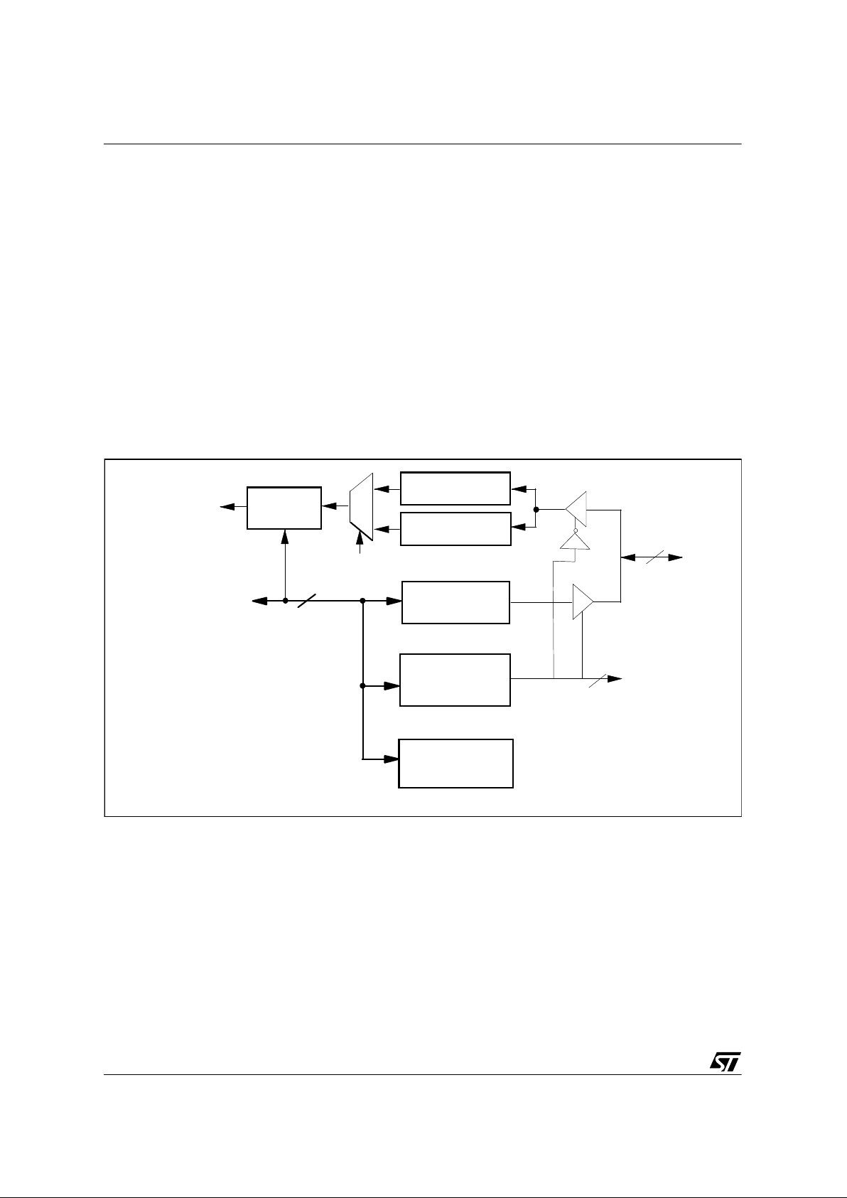
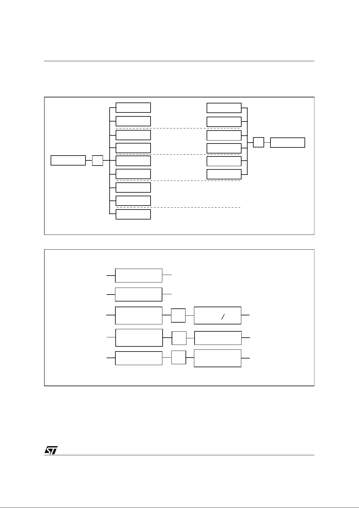
Figure 1.1 shows an architecture example for an AS-DSP used for audio decoding (Dolby
AC3, MPEG).
Figure 1.1 AS-DSP Architecture Example
DAT A
MEMORY
PROGRAM
MEMORY
PERIPHERAL A PERIPHERAL D
PERIPHERAL B PERIPHERAL C
CHANNEL 0
CHANNE L 1
CHANNEL 2
CHANNEL 3
DMA CONTROLLER
I
N
T
E
R
R
U
P
T
C
O
N
T
R
O
L
L
E
R
BUS
SWITCH
UNIT
D950-CORE
ON-CHIP MEMORY
ON-CHIP MEMORY
ON-CHIP MEMORY
X-BUS
I-BUS
Y-BUS
AS-DSP
TAP
VR02015
EMU
2

6/89
D950-Core
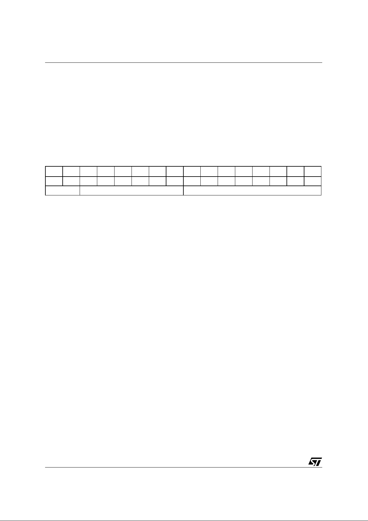
2 PIN DESCRIPTION
The following tables detail the D950-Core pin set. There is one table for each group of pins.
The tables detail the pin name, type and a short description of the pin function. A diagram of
the D950-Core I/O interface is contained at the end of the section.
Table 2.1 DATA BUSES (70 PINS )
Pin Name Type Descri pti on
XD0-XD15 I/O X Data Bus.
Hi-Z during cycles with no X-bus exchange.
XA0-XA15 O X Address bus.
Hi-Z when in Hold.
XRD
O X-bus read strobe. Active low.
Hi-Z when in Hold.
XWR
O X-bus write strobe. Active low.
Hi-Z when in Hold.
XBS
O X-bus strobe. Active low.
Hi-Z when in Hold.
Asserted low at the beginning of a valid X-bus cycle.
YD0-YD15 I/O Y Data Bus.
Hi-Z during cycles with no Y-bus exchange.
YA0-YA15 O Y Address bus.
Hi-Z when in Hold.
YRD
O Y-bus read strobe. Active low.
Hi-Z when in Hold.
YWR
O Y-bus write strobe. Active low.
Hi-Z when in Hold.
YBS
O Y-bus strobe. Active low.
Hi-Z when in Hold.
Asserted low at the beginning of a valid Y-bus cycle.
3

7/89
D950-Core
Table 2.2 PROGRAM BUS (35 PINS)
Table 2.3 BUS CONTROL (3 PINS)
Table 2.4 GENERAL PUR POSE P-PORT (9 PINS)
Table 2.5 CLOCK (4 PINS )
Pin Name Type Description
ID0-ID15 I/O Instruction data bus.
Hi-Z during cycles with no I-bus exchange.
IA0-IA15 O Instruction address bus.
Hi-Z when in Hold.
IRD
O I-bus read strobe. Active low.
Hi-Z when in Hold.
IWR
O I-bus write strobe. Active low.
Hi-Z when in Hold.
IBS
O I-bus strobe. Active low.
Hi-Z in Hold.
Asserted low at the beginning of a valid I-bus cycle.
Pin Name Type Description
DTACK
I Data transfer acknowledge. Active low.
Sampled on CLKIN rising edge.
Controls bus cycle extension by insertion of wait-states.
HOLD
I Hold bus request signal. Active low.
Asserted by a peripheral (DMA controller) requiring bus mastership. Halts
program execution and tri-states buses.
HOLDACK
O Hold Acknowledge output. Active low. Indicates that all buses are in Hi-Z.
Pin Name Type Description
P0-P7 I/O 8-bit bidirectional parallel port. Each pin can be individually programmed as
input or output and as level or falling edge sensitive input conditions for test
by branch and conditional instructions.
P_EN O Direction of Port
Pin Name Type Description
CLKIN I Clock input.
CLK_EMU I Emulation Clock input
DMA_CLK O DMA Clock output
BSU_CLK O BSU Clock output
3

8/89
D950-Core
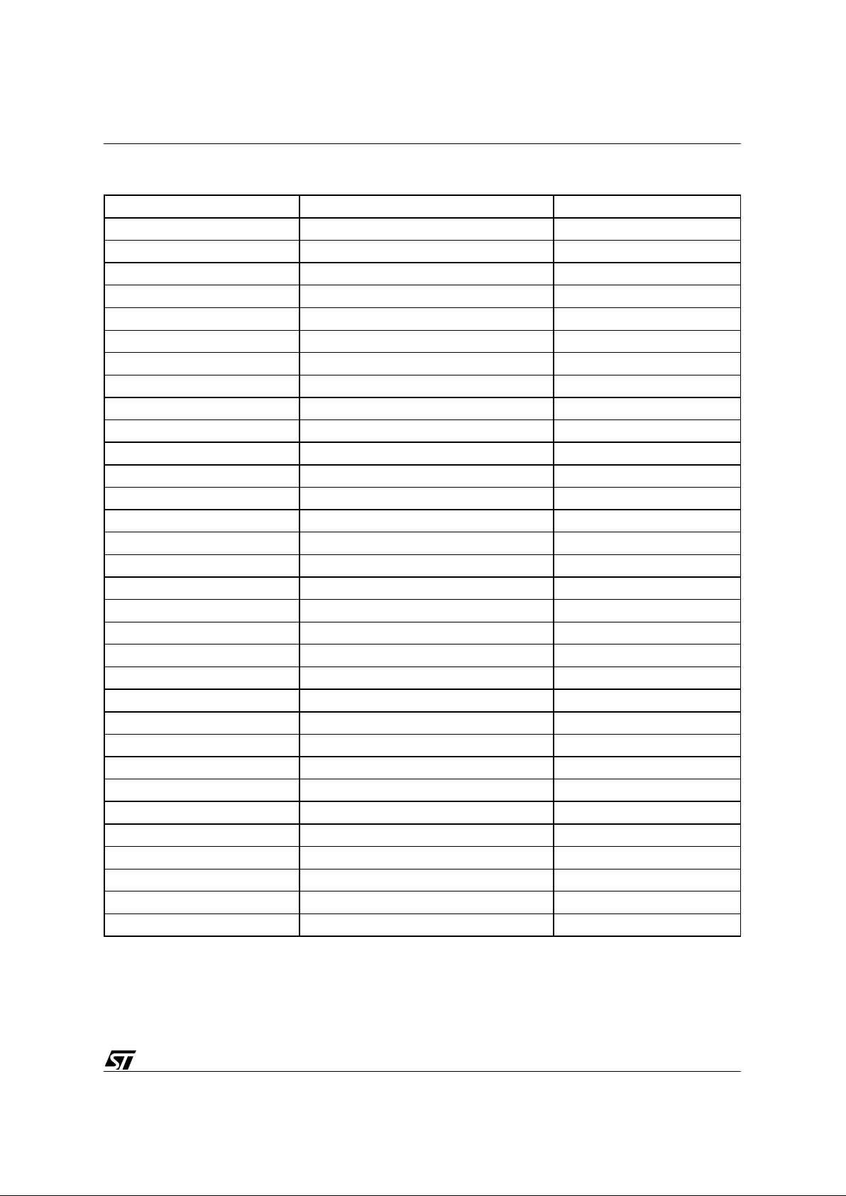
Table 2.6 CONTROL (13 P IN S)
Pin Name Type Description
IT
I Maskable Interrupt Request Input. Falling edge sensitive.
ITACK
O Maskable Interrupt Request Acknowledge. Active Low.
Asserted low at the beginning of Interrupt servicing.
EOI
O End of maskable Interrupt routine output. Active low.
Asserted low at the end of current interrupt request processing.
LP
I Low power. Falling edge sensitive.
Stops the processor after execution of the currently decoded instruction and
enters low-power standby state (in this state, the clock generator is stopped
except for INCYCLE).
LPACK
O Low power Acknowledge. Active low.
Asse rted low at the en d of ex ecut ion of the l ast in str ucti on following dete ction of LP
falling edge or at the end of LP or STOP instruction.
RESET
I Reset input. Active low.
Initializes the processor to the RESET state and the clock generator. Forces
Program Counter value to reset address and execution of NOP instruction.
MODE I Mode input select.
Forces reset address to 0x0000 (resp. 0xFC00) when low (resp. high).
VCI O Valid co-processor instruction decoded.
Asserted high while decoding a co-processor dedicated instruction. Indicates that the c o- pr oc e s s or inst ru c t ion w ill be ex ec u t ed at th e following instruction cycle.
IRD_WR O Indicates program memory RD/WR cycle during execution of Read or Write
Program memory instruction.
INCYCLE O Instruction cycle . Asserted high at the beginning of cycle.
RESET_OUT
O Hardware and Software Reset Output
STACKX O X Stack read/write instruction
STACKY O Y Stack read/write instruction
3

9/89
D950-Core
Table 2.7 EMULATION (9 PI NS)
Table 2.8 TAP CONTROLLER INTERFACE (10 PINS)
Table 2.9 SUPPLY (2 PINS)
Pin Na m e Type De sc ription
ERQ
I Emulator Halt Request. Active low.
Halts program execution and enters emulation mode.
IDLE O Output flag indicating if the processor is halted or executing an instruction
in Emulation mode.
HALTACK O Halt Acknowledge. Active high. Asserted high when the processor is halted
and under control of the emulator.
SNAP O Snapshot output. Active high. Asserted high when executing an instruction
in Snapshot mode.
HALT I Halt program execution request
EMI I Single Instruction Execute Comma nd
MCI O Multicycle in stru ction flag
IDLE O Execution of emulation instruction/Halted
FNOP O Forced NOP instruction flag
Pin Name Type Description
TE I Test Enable
TEST I Test Scan Mode
TI_ACU I Test Input for ACU
TO_ACU O Test Output for ACU
TI_PCU I Test Input for PCU
TO_PCU O Test Output for PCU
TI_DCU I Test Input for DCU
TO_DCU O Test Output for DCU
TI_CORE I Scan Chain input
TO-CORE O Scan Chain output
Pin Name Type Description
V
DD
I Positive Supply.
V
SS
I Ground pin.
3

10/89
D950-Core
Figure 2.1 D950-Core I/O Interface
D950-CORE
16
16
ID
IA
P
R
O
G
R
A
M
B
U
S
P0-P7
8
X-BUS
CLOCK
CLKIN
CLK_EMU
DMA_CL K
BSU_CLK
XA XD
16 16
Y-BUS
YA YD
1616
3
3
3
P-PORT
IRD / IWR / IBS
XRD / XWR / XBS
YRD / YWR / YBS
HOLDACK
DTACK / HOLD
BUS CONTROL
CONTROL
IT
LP
RESET
MODE
ITACK
EOI
LPACK
VCI
IRD_WR
INCYCLE
RESET_OUT
STACKX
STACKY
TEST & EMULATION
2
4
9
Ti_ACU
Ti_DCU
Ti_PCU
Ti_CORE
4
VR02016
8
P_EN
2
2
HALTACK
SNAP
IDLE
MCI
FNOP
5
ERQ
1
2
TE
TEST
TO_ACU
TO_DCU
TO_PCU
TO_CORE
4
2
HALT
EMI
3

11/89
D950-Core
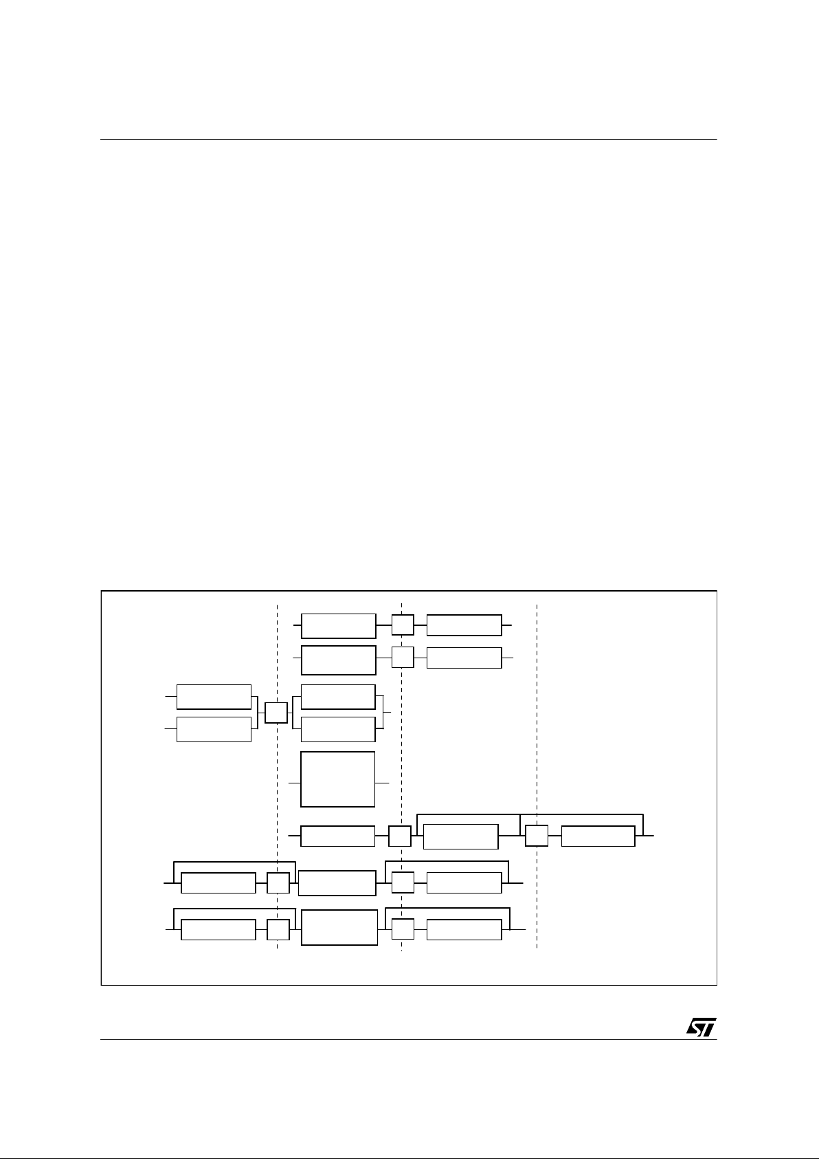
3 FUNCTIONAL OVERVIEW
The D950-CORE is composed of three main units.
• Data Calculation Unit (DCU)
• Address Calculation Unit (ACU)
• Program Control Unit (PCU)
These units are organized in an HARVARD architecture around three bidirectional 16-bit
buses, two for data and one for instruction. Each of these buses is dedicated to an unidirectional 16-bit address bus (XA/YA/IA).
An 8-bit general purpose parallel port (P0-P7) can be configured (input or output). A test
condition is attached to each bit to test external events. Each of these functional blocks are
discussed in detail in Section 4“BLOCK DESCRIPTION”.
Control of the chip is performed through interface pins related to interrupt, low-power mode,
reset and miscellaneous functions.
Clock input is provided on the CLKIN pin which is buffered to the output clocks.
Figure 3.1 Block Diagram
DATA
CALCULATION
UNIT
ADDRESS
CALCULATION
UNIT
PROGRAM
CONTROL
UNIT
CLKIN
DATA MEMORY
PROGRAM MEMORYVDD
VSS
TEST & EMULATIONPO/P7
CONTROL
11
8
14
XD-bus
YD-bus
6
16
16
16
16
3
16
16
OUTPUT
CLOCKS
XA-bus
YA-bus
ID-bus
IA-bus
4

12/89
D950-Core
Data buses (XD/YD and XA/YA) are provided externally. Data memories (RAM, ROM) and
peripherals registers are to be mapped in these address spaces.
Instruction bus (ID/IA) gives access to program memory (RAM, ROM). Each bus has its own
control interface
Table 3.1 Data/Instruction Bus and Corresponding Address B us.
Depending on the calculation mode, the D950-Core DCU computes operands which can be
considered as 16 or 32-bit, signed or unsigned. It includes a 16 x 16-bit parallel multiplier able
to implement MAC-based functions in one cycle per MAC. A 40-bit arithmetic and logic unit,
including a 8-bit extension for arithmetic operations, implements a wide range of arithmetic
and logic functions. A 40-bit barrel shifter unit and a bit manipulation unit are included.
Tables 3.2 and 3.3 illustrate the different types of word length and w ord format available for
manipulation.
Table 3.2 Summary of Possible Word L eng t hs
Data / Instruction Buses Corresponding Address Bus
XD Bidirec tional 16-bit XA Unidirectional 16-bit
YD Bidirec tional 16-bit YA Unidirectional 16-bit
ID Bidirectional 16-bit IA Unidi rectional 16-bit
01-bit word
7 0 8-bit word
15 0 16-bit word signed / unsigned
31 16 15 0 32-bit word signed / unsigned
39 32 31 16 15 0 40-bit word signed / unsigned
Table 3.3 Summary of Possible Word F or mat s
Format Minimum M aximum
fractional signed - 1 + 0.999969481
unsigned 0 + 0.99996948
integer signed - 32768 + 32767
unsigned 0 + 65535

13/89
D950-Core
4 BLOCK DESCRIPTION
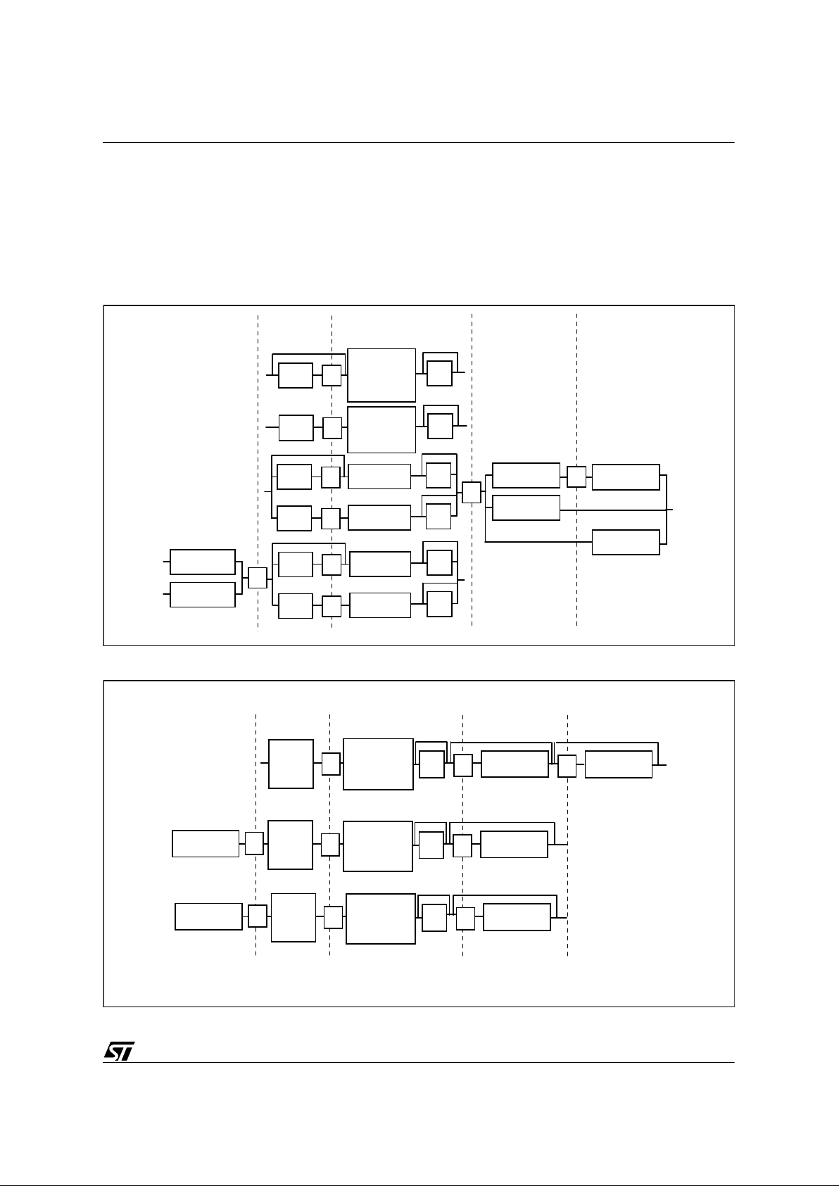
4.1 Data Calculation Unit (DCU)
4.1.1 Introduction
The D950-Core DCU includes the following main components:
• Register file - containing 16 data registers
• 4 Control Registers:
• DCU0CR: Register
• BSC: Shifter Control
• PSC: Shifter Control
• CCR: ALU Flags
• Multiplier - 16x16-bit signed/unsigned fractional/integer parallel multiplier.
• BSU - 40-bit Barrel Shifter Unit with a maximum right or left shift value of 32.
• ALU - 40-bit Arithmetic and Logic Unit implementing a wide range of arithmetic
and logic functions with an 8-bit extension for arithmetic operations.
• BMU - 16-bit Bit Manipulation Unit implementing bit operations on internal
registers and/or on 16-bit data RAM with an 8/16-bit mask.
Figure 4.1 D950-Core Data Calculation Unit
L0
L1
R0
R1
1616
XD YD
16-bit PL
16
16-bit A0H 16-bit A0L
16-bit A1H
16-bit A1L
40-bit A.L.U.
16-bit PH
32
XD
YD
6
32
C.C.R.
STA
8XD8
YD
8-b A0E
8-b A1E
13
328
B.S.C.
P.S. C.
6
16
16 x 16 SIGNED / UNSI GNE D
MULTIPLIER
WITH PROGRAMMABLE
ROUNDING
16
16
8
1313
8
16
40-bit extension
40-bit extension
40-bit B.S.
40
VR02017B
5

14/89
D950-Core
4.1.2 Registers
There are two types of registers: data registers and control registers. All registers are direct
addressed. Registers can be read or written through the X and Y buses. All of the D CU par ts
(multiplier, BSU, ALU, BMU) operate on these registers.
Data registers
L0 / L1: 2 x 16-bit input Left registers.
R0 / R1: 2 x 16-bit input Right registers.
A0 / A1: 2 x 40-bit Accumulators, each made of the concatenation of an 8-bit extension
A0E (resp. A1E), a 16-bit MSB A0H (resp. A1H) and a 16-bit LSB A0L (resp. A1L).
These registers are dedicated to extended precision calculations, in order to
provide up to 240 dB of dynamic range.
P: 32-bit multiplier result register made of the concatenation of PH (MSB) and PL
(LSB) 16-bit registers
Table 4.1 Data Register Structure.
L L1 L0 32-bit Input Left
31 16 15 0
R R1 R0 32-bit Input Right
31 16
A0 A0E A0H A0L 40-bi t Accu mulator 0
39 32 31 16
A1 A1E A1H A1L 40-bi t Accu mulator 1
39 32 31 16 15 0
P PH PL 32-bit Multiplier Result
31 16 15 0
L L1 0 16-bit Input Left
31 16 15 0
L L0 0 16-bit Input Left
31 16 15 0
R R1 0 16-bit Input Right
31 16 15 0
R R0 0 16-bit Input Right
5

15/89
D950-Core
Control regist ers
CCR: B its 0 to 12 are dedicated to the DCU (see Section 4.5.2).
BSC: 6-bit Barrel Shifter Control register. The BSC contains a 6-bit signed shift value
(2’s complement). If the value is positive (resp. negative), all shifts using the
BSC contents will provide a left (resp. r ight) shift. After rese t, the BSC val ue is
0.
PSC: 6-bit Product Shift Control register . T he PSC contains a 6-bit signed shift value.
If the value is positive (resp. negative) there will be a left (resp. right) shift on
the P-register. After reset, the PSC value is 0.
DCU0CR: Bits 0 to 7 are copied from bits 0 to 7 of the STA register. Bit 10 is used for
clearing the lower part (bits 0 to 15) and sign extending bits 32 to 39 of the
accumulator when its higher part (bits 16 to 31) is loaded.
4.1.3 Multiplier
The D950-Core multiplier performs 16 x 16-bit multiplications with the following
implementations (see SL and SR bits of STA register):
The 16 or 32-bit operands, are provided by a subset of the register file and stored in L1/L0 and
R1/R0, and accessed through X and Y buses.
The multiplication is performed in one single instruction cycle and the result is loaded in the
32-bit P register. The product can be either integer or fractional (see I-bit of STA register).
Rounding of the product is explicitly defined by the multiplication instructions (see Section
5.4.2).
SL LL SR LR Multipl ication
0 X 0 X Unsigned L-source X Unsi gned R-sourc e
1 0 0 X Signed L-source X Uns i gned R-sourc e
0 X 1 0 Unsigned L-source X S ig ned R-source
1 0 1 0 Signed L-source X Signed R-source
SL 1 SR X Unsigned L0 X Uns ig ned R-source
(dep on SR-bit)
or
Signed/Unsigned L-source X Signed/Unsigned R-source
SL X SR 1 Signed/Unsigned L-source
(depending on SL-bit)
X Unsigned R0
or
Signed/Unsigned L-source Signed/Unsigned R-source
IProduct
0 Fractional L-source X Fractional R-source
1 Integer L-source X Integer R-source
5

16/89
D950-Core
4.1.4 Barrel Shifter Unit (BSU)
The D950-Core BSU provides a complete set of shifting functions
Arithmetic shift: 40-bit input (either a 32 bit operand sign extended to 40-bit, or a 40-bit
accumulator), providing a valid result
Logical shift: provides a 32-bit result which is loaded into a 40-bit accumulator, the 8-bit
extension of which is reset.
Rotation:
8-bit EXT/sign 16-bit MSB 16-bit LSB
TST
8-bit EXT/sign 16-bit MSB
16-bit LSB
0
TST
Right: shi fts the 40-bit input data to the right , the upper part is sign extended
Left: shifts the 40-bit input data to the left, the upper part is fed by 0
8-bit EXT = 0 16-bit MSB 16-bit LSB
TST
8-bit EXT = 0 16-bit MSB 16-bit LSB
0
TST
Right: shi ft s the 32-bit in put data to the ri ght, the upper part is fed by 0
Left: shifts the 32-bit input data to the left, the upper part is fed by 0
0
8-bit EXT = 0 16-b it MSB 16-bit LSB
16-bit MSB 16-bit LSB
TST
Right: rot ates the inpu t data to the right (only thr ough the BSC register)
Left with TST: rotate s t he 33-bit data made of the concatenation of TST-bit
0
Left: rotates the 32-bit input data to the left
TST
of CCR with the 32-bit input data to the left (the LSB of the 32-bit input is
fed by TST-bit, the MSB of the 32-bit input fe eds the TST-bit of CCR).
5

17/89
D950-Core
When using a pure shift instruction, the T ST bit of th e CCR is fed by the last bit shifted out.
The shift value provided to the BSU is a signed value which may be provided i n three different
ways:
• By the instruction (shift defined in the instruction: see Section 5.4.2).
• By the BSC register (shift defined in the ALU code: if BSC c ontains a positive
(resp. negative) value, all shifts using BSC content will provide a left (resp.
right) shift).
• By the PSC register (shift defined in the MAC instruction: if PSC contains a
positive (resp. negative) value, all shifts using BSC content will provide a left
(resp. right) shift).
4.1.5 Arithmetic and Logic Unit (ALU)
The D950-Core ALU is 40-bit wide and implements about s ixty ALU functions. It i ncludes an
8-bit extension for arithmetical operations.
The calculation mode is controlled by both the instruction and the corresponding bits of the
STA register (see Section 4.5.1). The ALU has two inputs (see Figure 4.2), the left (always
the output of the BSU) and the right (fed by the registers making up the register file).
For logical operations, the ALU is fed with 32-bit wide operands, 0-extended to 40-bits. Then,
the ALU generates a 40-bit result which is always stored in A0 or A1 (A0E and A1E extension
registers being reset).
For arithmetical operations, the ALU is fed with 40-bit wide operands.
• If the operand is an accumulator, the entire 40-bit register (A0E/A0H/A0L or
A1E/A1H/A1L) feeds the 40-bit ALU.
• If not, the 32-bit register is considered as sign extended to a 40-bit format. The
extended ALU then generates a 40-bit wide result which is always stored in
A0E/A0H/A0L or A1E/A1H/A1 L
Figure 4.2 D950-Core ALU Operations
A0 or A1
40-bit A.L.U.
40
40
8-bit
16-bit 16-bit
FROM BSU
FROM
REGISTER
FILE
16 16
CCR
13
8
VR02017C
5

18/89
D950-Core
The ALU output is always made to one of the two accumulators and the CCR (with the
exception of particular ALU codes which affect only CCR or an accumulator). The ALU
operations can be partitioned into three different groups (see Section 5.4.2), depending on the
number of operands the operation requires:
Specific ALU codes (see Section 5.4.2) are used to implement a non-restoring conditional
add/subtract division algorithm. The division can be signed or unsigned. The dividend must be
a 32-bit operand sign extended to 40-bit and located in the 40-bit accumulator. The divisor
must be a 16-bit operand located in R0 or R1 (LR-bit of STA register must be low).
In order to obtain a valid result, the absolute value of the dividend must be strictly smaller than
the absolute value of the divisor (considering operand is in a fractional format).
Special features are implemented in the D950-Core to process multi-precision data (see
DMULT instruction for double-precision MAC operations).
Two overflow preventions exist in the D950-Core (see SAT and ES bits of STA register):
1: For the multiplier, when multiplying 0x8000 by 0x8000 in signed/signed fraction-
al mode, the saturation block forces the multiplier result to 0x7FFFFFFF,
2: For the ALU, when the result overflows. Provided one of the two optional satu-
ration modes (32-bit saturation or 40-bit saturation) has been selected, the accumulator destination is set to plus or minus the maximum value.
Two rounding operations are enabled in the D950-Core (see RND-bit of STA register):
1: The multiplier result stored in P register explicitly defined by the instruction. A
two’s complement rounding is performed on the result which is s tored in the 16bit PH register (see Section 5.4.2).
2: The 40-bit accumulator (either two’s complement or convergent rounding) pro-
vided by ALU operation (see RND-bit of STA register).
4.1.6 Bit Manipulation Unit (BMU)
The BMU allows bit m anipulation operations on 16-bit data sources, access ed in 3 different
modes: direct, indirect and register addressing, through dedicated instructions.
An 8-bit mask is applied to enable the following operations on a bit-per-bit basis:
• TSTL: bit test low.
• TSTH: bit test high.
• TSTHSET: bit test high and set.
• TSTLCLR: bit test low and reset.
ALU Code Number of So urces Number of D es tin a tio ns
3 operands 2 1
2 operands 1 1
1 operand 1 (source=destination) 1 (source=destinat ion)
5

19/89
D950-Core
Figure 4.3 D950-Core Bit Manipulation Unit
This 8-bit mask is extended to a 16-bit mask in three ways:
• 8-bit value on MSBs, 0x00 on LSBs,
• 0x00 on MSBs, 8-bit value on LSBs,
• 8-bit value on MSBs, 8-bit value on LSBs. (In this case, the mask value is the
same on MSB and LSB.)
For registers with a length less than 16-bit (AIE, BSC, PSC), the signed v alue data is signextended to a 16-bit signed value data before being tested.
Figure 4.4 Extension of an 8-bit Mask to 16-bit Mask
Figure 4.5 S ign Extension to a 16-bit Signed Value
15 8 7 0
MASK 0
0MASK
MASK MASK
16
8
16
INTERNAL REG ISTER
RAM
EXTENSION
TST
BIT MANIPULATION
UNIT
MASK
Processed D ata
VR020 17 D
VR02017P
S
0
15
5

20/89
D950-Core
4.2 Address Calculation Unit (ACU)
4.2.1 Introduction
The D950-Core ACU includes two id entical address generators (one for each data memory
space), each containing:
• 2 x 16-bit address registers
• 4 x 16-bit index registers
• Adder for address register update
• 2 x 16-bit base and maximum address registers for modulo addressing. There
is dedicated logic for address comparison and calculation.
Figure 4.6 D950-Core Address C alculation Unit
In addition to these two address generators, the D950-Core ACU includes:
• 16-bit Stack Pointer (SPX) register for the X-memory space mapped stack
• 16-bit Stack Pointer (SPY) register for the Y-memory space mapped stack
• 6 bits of STA register for addressing modes
VR02017E
STA
6
AY0
AY1
BY
MY
MODULUS
LOGIC
16-bit ADDER
IY0
IY1
IY2
IY3
6
16
16
16
16
AX0
AX1
BX
MX
MODULUS
LOGIC
16-bit ADDER
IX0
IX1
IX2
IX3
SPX
XD
XA
YD
YA
SPY
5

21/89
D950-Core
4.2.2 Registers
The D950-Core ACU includes two types of registers: data registers and control registers
Data registers:
The following registers are directly addressed by instructions:
• 2 x 16-bit pointer registers and 4 x 16-bit index registers are dedicated for each
data memory space:
• AX0/AX1 (pointer), IX0/IX1/IX2/IX3 (index) for X-memory space,
• AY0/AY1 (pointer), IY0/IY1/IY2/IY3 (index) for Y-memory space.
In addition to these registers, 16-bit SP registers address the stacks located in the X and Ymemory spaces.
The following four registers are mapped in Y-memory space:
• 2 x 16-bit base and maximum address registers are dedicated for each Data
memory space:
• B X (Base), MX (Maximum) for X-memory space,
• B Y (Base), MY (Maximum) for Y-memory space.
Control Register:
STA: Bits 8 to 13 are dedicated to ACU ( see Section 4.5.1 ). Index register values are 16-bit
signed.
4.2.3 Addressing modes
The D950-Core provides the following addressing modes:.
Addressing Modes Type
DIRECT
INDIRECT
LINEAR POST- INCREMENT
MODULO POST-INCREMENT
BIT-REVERSE POST-INCREMENT
INDEXED
IMMEDIATE
STACK
5

22/89
D950-Core
Direct addressing
Memory direct addressing instructions require one extension word to provide the memory
address, and are executed in two cycles. They are used for data moves between memory and
direct addressable registers.
Registers addressable by the instruction code include:
• 16 for DCU (L1/L0/R1/R0/A1E/A1H/A1L/A0E /A0H/A0L/PH/PL/BSC/PSC/STA/
CCR),
• 13 for ACU (AX0/AX1/IX0/IX1/IX2/IX3/AY0/AY1/IY0/IY1/IY2/IY3/SPX),
• 3 for PCU (LS/LC/LE).
Figure 4.7 Direct Addressing
Indirect addressing
See RX1, RX0, MY1, MY0, MX1 and MX0 bits of the STA register. The instruction specifies
the address register (AX0, AX1, AY0, AY1) of the operand to process, and the address
calculation to be performed, according to STA register content.
At the end of the instruction, the new address register (AXi / AYi) contains the previously
selected address (AXi / AYi), post-incremented by the corresponding index registers (IXi / IYi).
Four types of indirect addressing modes are implemented:
1: Linear addressing with post-modification.
Address modification is done using the normal 16-bit 2's complement linear
arithmetic.
2: Modulo addressing with post-modification.
This mode can be selected individually for AX0, AX1, AY0, AY 1 registers (see
MX0, MX1, MY0, MY1 bi ts of STA register).
BX / MX: 16-bit register Base / Maximu m address for AX0 / AX1,
BY / MY: 16-bit register Base / Maximu m address for AY0 / AY1.
Base and maximum addresses can be defined to any value, provided that: the
maximum address is greater than base address, the starting address is initialized within the base/maximum address range, the index absolute value is less
than or equal to maximum address minus the base address.
register
value
address
Memory
VR02017F
5

23/89
D950-Core
3: Bit reverse addressing (on X-memory space only) with post-increment
This mode can be selected for AX0, AX1 (see RX0, R X1 bits of STA register).
It generates the bit-reversed address for 2k point FFT implementation (Index
value = 2k-1).
4: Indirect indexed addressing. The address of the operand is the sum of the con-
tents of the address register (AXi, AYi, SPX or SPY) and the contents of the selected index register (IXi or IYi). This addition occurs be fore the operand is accessed and therefore requires an extra instruction cycle. The contents of the selected address and index registers are unchanged.
Figures 4.8 and 4.9 show the schematics for indirect addressing with and without post
modification.
Figure 4.8 Indirect Addressing with Post-Modification
Figure 4.9 Indirect Indexed Addressing wit hout Post-Modification
register
value address
Memory
- linear
- bit-reverse
- modulo
+
index reg.
address reg.
VR02017H
register
value
address
Memory
- linear
+
index reg.
address reg.
VR02017G
5

24/89
D950-Core
Immediate Data Addressing
This mode allows direct register loading. If the data is 16-bit long (see LR and LL bits of STA
register), this mode requires one word of instruction extension to store the data.
Immediate short data addressing is possible on 6-bit data, without instruction extension:
If AXi, AYi or STA are concerned, the 6 LSB’s are loaded from the instruction and the MSB’s
are unchanged. For all other registers, the MSB’s are fed with 0
Figure 4.10 Immediate Addressing
Stack operation addressing
16-bit Stack Pointer register SPX is available for X-memory space and SPY for Y-memory
space. It can be initialized to any val ue, pr ovide d it points to a stack dedicated memory area.
The stack size is limited to the available memory. No provision is taken to detect stack
overflows or underflows. After reset, the SP registers are not initialized.
The following addressing modes are possible with the 16-bit SP registers:
• For the X and Y stack pointer registers: PUSH (SP pre-decrement) or POP (SP
post-increment) for register-to-stack move, memory-to-stack move and for
immediate value-to-stack move.
Double PUSH and double PO P. In th is operation, the PUSH or PO P operation
is performed simultaneously on the X and Y stack point register. This is used in
a switching context.
• For the X stack pointer register only: Indirect indexed addressing for registerto-stack move.
register
value
VR02017I
5

25/89
D950-Core
4.3 Program Control Unit (PCU)
4.3.1 Introduction
The D950-Core PCU includes the following components:
• 16-bit Program Counter (PC)
• 9 x 16-bit Loop registers (3 x LS, 3 x LE, 3 x LC)
• Branch and Hardware Loops control logic including CCR and PORT condition
decoding
• 2 bits of STA register for interrupt control
• 2 bits of CCR for loop management
• Reset, Hold and Low-Power operation control logic
• Stack control logic for automatic PC save and restore in Subroutine Calls and
Interrupts. (The Stack is implemented in a user-defined dedicated X-RAM
area. The Stack pointer and its control logic are included in the ACU, see
Section 4.2.1.)
•PPort
Figure 4.11 D950-Core Program Control Unit
XRAM
STACK
SPX
16
CONTROL
IR
MUX
IA
ID
LS0:2
LE0:2
LC0:2
LS
YD
XD
16
16
RESET
+ 1
BRANCH / IT @
RTS / RTI @
LOOP
REGISTERS
TO OTHER UNITS
CCR COND. (13)
PORT COND. (8)
16
16
16-BIT
PC
STA
2
2
RESET
IT
LP
HOLD
VR02017J
8
P.PORT
PORT COND
8
P8P_EN
5

26/89
D950-Core
4.3.2 Registers
Data registers
• LS0 / LS1 / LS2: 3 x 16-bit Loop Start address registers,
• LE0 / LE1 / LE2: 3 x 16-bit Loop End address registers,
• LC0 / LC1 / LC2: 3 x 16-bit Loop Count registers.
All these registers are addressed directly by the LSP instruction (see Section 4.3.5)
After reset, LSP = 0. (No hardware loop is selected).
Control regist ers
• STA: Bits 14 and 15 are dedicated to PCU (see Section 4.5.1).
• CCR: Bits 14 and 15 are dedicated to PCU (see Section 4.5.2).
4.3.3 Instruction pipeline
Instruction execution is performed in a 3-stage pipeline: fetch/decode/execute. While
instruction n is executed, instruction n+1 is decoded and instruction n+2 is fetched.
The instruction cycle period is twice the CLKIN period.
According to the number of words used, D950-Core instructions can be of two types
• One word instruction: Inside this group, most D950-Core instructions are one
cycle instructions (all arithmetic and logic instructions except instructions
performing double precision multiplication and bit manipulations). Some
instructions are multiple cycle instructions. Instructions causing a program flow
change (JUMP, CALL, RTS, RTI, SWI, RESET, BREAK, CONTINUE) are
executed in two or three cycles.
• Instructions with extension words : As one program m emory word is fetched
at each cycle, if an instruction needs extension words, they are fetched during
the cycles following the first fetch.
4.3.4 Interrupt Sources
The D950-Core includes three interrupt sources. The following table orders the interrupt
sources from highest to lowest priority
5

27/89
D950-Core
Table 4.2 Interrupt Sources and Priority
RESET
Non maskable (internally vectorized), either hardware or software (see Table 6.3.3“Hardware
Reset”)
In hardware, when a low level is applied to the RESE T
input, the CLOCK generator is resynchronized, the PC is reset, execution of NOP instructions is forced and control registers are
initialized.
In order to get a valid reset, a low level must be applied for a minimum of ten CLKIN cycles (i.e
five D950-Core cycles).
In software, the RESET instruction is a 3-cycle instruction having the same effects as a
hardware reset, except the CLOCK generator is not re-synchronized.
The reset address is 0x0000. By setting the MODE pin to 1, the alternate reset address
0XFC00 is selected.
INT
Maskable external interrupt EI and IPE bits of STA register (s ee Table 6.3.5“Interrupt”)
Start of Interrupt: External interrupt is disabled on reset and is enabled by setting EI-bit to 1.
As soon as an IT
falling edge is memorized and r ecognized by the PCU at the beginning of an
instruction cycle, IPE-bit is set. Provided IT
has been previously enabled, ITACK signal is
asserted low to acknowledge the interrupt. ITACK
stays at the low state for one cycle, allowing
the interrupt vector to be pr ovided by the controller on Y-bus. Then IPE -bit is reset. Interrupt
start processing requires three cycles to read the interrupt vector and to fetch the
corresponding instruction. Meanwhile, CCR register, STA and the return address are
automatically saved onto the stack, located in X-memory space.
Return from Interrupt: Return from the interrupt is performed by the RTI instruction, a 3-c ycle
instruction during which the return address, STA register and CCR are retrieved from the
stack. The EOI
signal is then asserted low, allowing the controller to arbitrate pending interrupt
requests and to issue, if required, the next interrupt request to the D950-Core.
An interrupt request that is recognized while decoding or executing a delayed branch
instruction, is not acknowledged until all operations related to the branch have been
completed.
In addition to this external interrupt source, a powerful interrupt controller is available as
peripheral of the D950-Core (see Section 7.3).
Sources Priority
RESET Non-Maskable Highest
SWI Non-Maskable
INT Maskable Lowest
5

28/89
D950-Core
SWI
Non maskable (internally vectorized) software interrupt SWI is a 3-cycle instruction whose
interrupt routine address is 0x0002. Return from the SWI routine is performed through RTI.
The SWI routine is non-interruptible by an external interrupt request.
Note: IT should not be asserted low if a previous request has not been acknowledged. In this case,
the previous request will not be processed.
EI and IPE bits are not affected when STA register is restored.
4.3.5 Loop Controller
Table 4.3 Loop Instruction
Hardware lo op resources
The program sequencer includes a powerful hardware loop mechanism. This allows the
nesting of up to three levels of loops by us ing nine 16-bit registers, organized in three banks
of three registers.
Each bank includes one loop start address r egister (LS), one loop end address register (LE)
and one loop count register (LC ). These registers can be r ead and written by register m ove
instructions, allowing extension of the number of nested loops by software.
The currently selected loop register bank is pointed to by bits LSP 1 and LSP0 of th e CCR.
When the current level changes, this 2-bit register is incremented or decremented through
dedicated instructions (see Section 5.4.5“Conditional Assignment Instruction”) to modify
the bank.
Loop operation: REPEAT instruction
The REPEAT instruction performs automatic management of the different loop registers (LS,
LC, LE and LSP) and defines the number of iterations and address of the last instruction of the
loop.
The loop begins at the instruction following REPEAT. Conditional instructions CONTINUE and
BREAK can be put within a loop. Their effect is to restart (resp. exit from) the loop when the
condition is verified.
Notes 1: The m aximu m repeat count value of 216-1 is obtained by setting LC to 0xFFFF.
2: An endless loop can be set up by initializing LC to: 0x0000 for REPEAT block,
0x0001 for REPEAT single.
Loop Instruction Body of loop Loop value
Single in str uc t io n Immed iate
REPEAT Block of instructions Immediate
Block of instructions Computed
5

29/89
D950-Core
4.3.6 Sequence control
The PC is incremented at every cycle when the program flow is linear. Non linear sequencing
occurs in the following cases:
• JUMP instructions
• CALL and RTS instructions (JUMP and CALL can be immediate or computed /
delayed or not / conditional or not)
• CCR bit and PORT bit can be tested
• Interrupts and RTI instruction.
• Processing of automatic loops.
Extension of the program memory space to more than 64k x 16-bit, can be achieved by
including a memory-mapped program page regi ster ( PPR) into the D950-Core glue logic. This
register is read or written to by move instructions.
Due to the pipe-line of instruction execution, changing page by loading a value into PPR will
be effective at the time of execution of the following instruction, which is read in the current
page. This operation will work properly if no interrupt oc curs between the P PR load and the
JMP.
To avoid the need to disable interrupts by software, before page change, a special memory
mapped register address has been defi ned for P PR at address 0x0062.Y . Whenever a write
with direct address or a POP with direct address i s attempted at thi s address, execution of the
following instruction can not be interrupted.
4.3.7 Halting program execution
There are 4 ways to halt program execution: low power mode, stop mode, hold state and halt
state. These 4 methods are detailed in the figure below and discussed in this section.
Figure 4.12 Halting Program Execution
RUN
HALT
HOLD
STOP
LOW POWER
(CLKOUT OF F)
(CLKOUT ON)
HALTACK
HALTACK
STOP
instruction
INTERRUPT
INTERRUPT
LP
instruction
HOLD
HOLD
LP pin
asserted
EMULATION RESOURCE SHARING
LOW POWER
(CORE / PERIPHERALS)
LOW POWER
(CORE ONLY)
H
A
R
D
W
A
R
E
S
O
F
T
W
A
R
E
5

30/89
D950-Core
Low Power Mode
There are two ways to enter the low power mode:
• Execution of LP instruction.
The LP instruction is a 3-cycle conditional instruction. The Low Power mode is
entered after the last execute cycle of the LP instruction.
• Driving LP
to low state.
LP
is falling edge sensitive. Low Power mode can be entered only if the
processor is not in HOLD state or in Emulation mode.
The instruction decoded at the time that a LP request is recognized, is executed. Entering Low
Power mode is acknowledged by driving LPACK
low.
When operating in Low Powe r mode, the D950-Core enters an idle state. In this state, the
following events occur:
• The clock generator is stopped (internal cycle clock) and INCYCLE remains
active. BSU_CLK, DMA_CLK ar e stopped.
• The internal state of the processor is frozen.
• X and Y data buses stay driven to Hi-Z.
• The bus address lines and control lines are driven to Hi-Z.
Exit of Low Power mode: Initiated by detecting a falling edge on IT
. The processor clock
generator is restarted and LPACK
is driven to a high st ate. If interrupts were di sabled, program
execution restarts from the current PC and interrupt handshake signals ITACK
and EOI are
not activated. If interrupts were enabled, a normal interrupt process starts.
STOP Mode
STOP mode is entered by use of the STOP instruction. The STOP instruction is processed as
the LP instruction, all clocks are stopped at the same time as the internal clock is stopped. The
LPACK
signal is activated in the same way as for LP instruction.
Exit of the STOP mode is performed by detection of an interrupt request with the same
conditions as for exit of LP. LPACK
signal is activated in the same way as for LP.
5

31/89
D950-Core
HOLD State
This function allows the release of the buses for another device such as a DMA controller (see
Section 6.3.6).
Entering HOLD state: The HOLD signal is sampled at the beginning of e very cycle. When
HOLD
is recognized low, the processor immediately releases the I-bus and then releases the
X and Y buses after execution of the currently decoded instruction. Bus address, data and
control lines are then tri-stated.
Program execution is stopped and HOLDACK
is asserted low during HOLD state.
Note:HOLD state can not be entered when the processor is in emulation mode.
Exit of HOLD state: The processor recovers bus mastership as soon as HOLD is sam pled
high and next instruction is fetched.
HALT State
This function is used in em ulation m ode only. It is us ed to stop progr am executi on by us e of
the peripheral emulator unit (see Section 7.5).
4.3.8 Memory Moves with Wait States
DTACK input is used to stretch instruction cycles, in order to access slower memory and/or
peripherals. DTACK
is sampled on the rising edge of CLKIN. If DTACK is high on the third
rising edge of the cycle, the cycle is extended by two CLKIN cycles (see Section 6.3.4).
Extension cycles are added by the clock generator until DTACK
is recognized low.
Note:DTACK generation can be controlled by the Bus Switch Interface peripheral (see Section 7.2).
5
32/89
D950-Core
4.4 General Purpose P-Port
4.4.1 Introduction
The P-Port is an 8-bit (P0/P7) general purpose parallel port in which each port pin can be
individually programmed as input (level or falling edge sensitive) or output.
1
The data direction and sensitivity for each bit are programmed through PCDR and PCSR 8-bit
registers.
Port inputs are sampled on each INCYCLE rising edge. Detection of a level change is
performed, provided the input remains at the same level for at least one INCYCLE cycle.
2
The Port input data is stored into the 8-bit Port Input Register (PIR). The Port output data is
stored into the 8-bit Port Output Register (POR).
3
Figure 4.13 D950-Core Parallel I/O Port
Notes 1: PPort can be used as a branch condition.
2: PIR value is set to 1 on falling edge detection,until the port is tested.
3: The significant bit are 8-LSBs (8-MSBs=undefined when reading).
PORT INPUT
REG. (PIR)
EDGE/LEVEL
SENSITIVITY
FALLING EDGE
DETECTION
LEVEL
DETECTION
PORT OUTPUT
REG. (POR)
PORT CONTROL
DIRE CTIO N REG.
(PCDR)
POR T CONT ROL
SENSITIVITY
REG. (PCSR)
YD
16
P0 / P7
PORT CONDITION
TO P.C.U.
8
VR02017N
8
P_EN
5

33/89
D950-Core
4.4.2 Registers
PCDR
The Port Control Direction register defines the data direction of each port pin. After reset,
PCDR default value is 0 (Port pins are configured as inputs).
PiD: Port pin direction
0: Input port pin (def.)
1: Output port pin
- : for bits 8 to 15 indicates RESERVED (read: undefined, write: don’t care)
PCSR
The Port Control Sensitivity register defines sensitivity of each port pin. After reset, PCSR
default value is 0 (Port pins are configured as level-sensitive).
PiS: Port pin sensitivity
0: Level sensitive (def.)
1: Edge sensitive
- : for bits 8 to 15 indicates RESERVED (read: undefined, write: don’t care)
1514131211109876543210
--------P7DP6DP5DP4DP3DP2DP1DP0D
1514131211109876543210
--------P7SP6SP5SP4SP3SP2SP1SP0S
5
34/89
D950-Core
4.5 Common Control Registers
4.5.1 STA: Status register
STA is a 16-bit status register shared by both the DCU, the ACU and the PCU.
Bits 0 to 7 are dedicated to DCU which defines the calculation mode for certain instructions
and specifies the type of operands to be used. Bits 8 to 13 are dedicated to the ACU w hich
initializes circular and bit-r everse addressing modes. Bits 14 and 15 are dedi cated to the PCU
which controls interrupts.
After reset, STA default value is 0x004C.
EI: Enable Interrupt
0: Interrupt is disabled (def.)
1: Interrupt is enabled
IPE: Interrupt Pending: Set and reset by software only using the bit manipulation instruc-
tion.
0: Reset by hardware when the interrupt is acknowledged (def.)
1: Set by hardware when the trigger event occurs or by the programmer to generate
an interrupt.
RX1: Bit reverse addressing mode for AX1
0: No bit reverse addressing mode for AX1 (def.)
1: Bit reverse addressing mode is selected for AX1
RX0: Bit reverse addressing mode for AX0
0: No bit reverse addressing mode for AX0 (def.)
1: Bit reverse addressing mode is selected for AX0
MY1: Modulo addressing mode for AY1
0: No modulo addressing mode for AY1 (def.)
1: Modulo addressing mode is selected for AY1. AY1 is updated through the Y-
memory space modulo logic.
MY0: Modulo addressing mode for AY0
0: No modulo addressing mode for AY0 (def.)
15 14 13 12 11 10 9 8 7 6 5 4 3 2 1 0
EI IPE RX1 RX0 MY1 MY0 MX1 MX0 RND ES SAT I SR SL LR LL
PCU ACU DCU
5

35/89
D950-Core
1: Modulo addressing mode is selected for AY0. AY0 is updated through the Ymemory space modulo logic.
MX1: Modulo addressing mode for AX1
0: No modulo addressing mode for AX1 (def.)
1: Modulo addressing mode is selected for AX1. AX1 is updated through the X-
memory space modulo logic.
MX0: Modulo addressing mode for AX0
0: No modulo addressing mode for AX0 (def.)
1: Modulo addressing mode is selected for AX0. AX0 is updated through the X-
memory space modulo logic.
RND: Rounding type for ALU operation
0: Convergent rounding (def.)
1: Two’s complement rounding
ES: Extended Saturation
0: The saturation is active when a 32-bit overflow occurs (if SAT=1)
1: The saturation is active when a 40-bit overflow occurs (if SAT=1) (def.)
SAT: Saturation
0: ALU is not in saturated mode (def.)
1: ALU is in saturated mode
I: Integer Product
0: Product is in fractional format (if signed * signed, one bit is shifted left before storing
the result into P register) (def.)
1: Product is in integer format (no shift and direct transfer into P register)
SR: Right side operand type (only used for product calculation and division)
0: Right side operand is unsigned
1: Right side operand is signed (def.)
SL: Left side multiplicand type (only used for product calculation)
0: Left side multiplicand is unsigned
1: Left side multiplicand is signed (def.)
LR: Right side long data
0: Normal 16-bit data mode (def.)
5
36/89
D950-Core
1: Data contained in R0 and R1 is long 32-bit data (the 16 MSB’s in R1, the 16 LSB’s
in R0)
LL: Left side long data
0: Normal 16-bit data mode (def.)
1: Data contained in L0 and L1 is long 32-bit data (the 16 MSB’s in L1, the 16 LSB’s in
L0)
4.5.2 CCR: Condition Code Register
CCR is a 16-bit register shared by both the DCU (bits 0 to 12) and the PCU (bits 14 and 15).
This register is affected each time an ALU operation occurs, and gives information on the last
result stored in A0 or A1 accumulator.
After reset, CCR default value is 0.
LSP1/LSP0 Loop Stack Pointer
00: No loop / Bank 1 (def.)
01: Loop level 1 / Bank 1
10: Loop level 2 / Bank 2
11: Loop level 3 / Bank 3
TST: Result of the test instructions in bit manipulation or last bit shifted out in pure shift
operations
C31: Carry value generated out of bit 31 during the last ALU operation (always loaded
except for DMULT instruction)
NQ: 1’s complement of next quotient bit (only affected by DIVS and DIVQ instructions)
CS: Compared sign updated by CMPS instruction as the XOR of the two ALU operand
signs (bit 31) (used also by DIVS, RESQ and RESR instructions)
PAR: Parity of the last ALU resu lt.
0: Bit 16 of the last 40-bit ALU result is 0 (def.)
1: Bit 16 of the last 40-bit ALU result is 1
MN: Memorized normalized
0: Reset when tested by a conditional instruction (def.)
1: Set when ALU result is normalized
1514131211109876543210
LSP1 LSP0 - TST C31 NQ CS PAR MN N EXT MOVF OVF Z C S
PCU - DCU
5

37/89
D950-Core
N: Normalized
0: ALU result is not normalized (def.)
1: ALU result is normalized (bits 31 to 39 are equal & opposed to bit 30)
EXT: Extension
0: The 8-bit extension is the sign of the 32-bit ALU result
1: The last ALU result overflows the 32-bit format
MOVF:Memorized overflow
0: Reset when tested by a conditional instruction (def.)
1: Set when the last ALU result overflows the 40-bit format
OVF: Overflow
0: An arithmetic overflows does not occur for the last 40-bit ALU result (def.)
1: An arithmetic overflow occurs for the last 40-bit ALU result
Z: Zero
0: ALU result is different from zero (def.)
1: ALU result is zero
C: Carry value generated out of bit 39 during the last ALU operation
S: Sign
0: ALU result is positive (def.)
1: ALU result is negative
Note:‘-’ for bit 13 indicates RESERVED (read: 0, write: don't care)

38/89
D950-Core
Table 4.4 Table of Conditions
Notation Description
ALWAYS NEVER
Test of CCR bits
Z NOZ Zero bit of CCR
LT GTE S XOR OVF bits of CCR
LTE GT (S XOR OVF) OR Z bits
C NOC Carry bit of CCR (bit 39)
S NOS Sign bit of CCR
EXT NOEXT Extension bit of CCR
OVF NOOVF Overflow bit of CCR
MOVF NOMOVF Memorized overflow
N NON Normalised bit of CCR
MN NOMN Memorized Normalised
PAR NOPAR Parity bit of CCR
C31 NOC31 Carry bit of CCR (bit 31)
TEST NOTEST Test bit of CCR
Test of Port bit s
P0 NOP0 Bit 0 of Parallel Port
P1 NOP1 Bit 1 of Parallel Port
P2 NOP2 Bit 2 of Parallel Port
P3 NOP3 Bit 3 of Parallel Port
P4 NOP4 Bit 4 of Parallel Port
P5 NOP5 Bit 5 of Parallel Port
P6 NOP6 Bit 6 of Parallel Port
P7 NOP7 Bit 7 of Parallel Port
39/89
D950-Core
Table 4.5 Direct Address Register Table
Note: Memory mapping is described in the appendix (see Section 8)
Register Na m e Function Location
AX0 X address register ACU
AX1 X address register ACU
AY0 Y address register ACU
AY1 Y address register ACU
IX0 X index register ACU
IX1 X index register ACU
IX2 X index register ACU
IX3 X index register ACU
IY0 Y index register ACU
IY1 Y index register ACU
IY2 Y index register ACU
IY3 Y index register ACU
SPX Stack Pointer register ACU
LS Loop Start register PCU
LC Loop Count register PCU
LE Loop End register PCU
L0 DCU input left register (LSB) DCU
L1 DCU input left register (MSB) DCU
R0 DCU input right register (LSB) DCU
R1 DCU input right register (MSB) DCU
PL Product register (LSB) DCU
PH Product register (MSB) DCU
CCR Condition Code Register DCU
STA Sta tus register DCU
A0L Accumul ator 0 (LSB) DCU
A0H Ac cumulator 0 (MSB) DCU
A0E Accumulator 0 (Extension) DCU
BSC Barrel Shifter Control register DCU
A1L Accumul ator 1 (LSB) DCU
A1H Ac cumulator 1 (MSB) DCU
A1E Accumulator 1 (Extension) DCU
PSC Product Shift Control register DCU

40/89
D950-Core
5 SOFTWARE ARCHITECTURE
5.1 Introduction
Instruction execution is performed in a 3-stage pipeline: fetch/decode/execute. While
instruction n is executed, instruction n+1 is decoded and instruction n+2 is fetched. The
instruction cycle period is twice the CLKIN period. According to the number of words used,
D950-Core instructions can be of two types: one word intructions or extension word
instructions.
One Word Instructions:
Most of D950-Core instructions are one cycle instructions:
• All arithmetic and logic instructions with or without parallel data moves,
excepted instructions performing double precision multiplication and bit manipulations.
• Register to register data move.
• Memory to register indirect data move.
The following are multiple cycle instructions:
• Double precision MAC (two cycles).
• Indirect indexed register move (two cycles).
• Indirect indexed register to stack move (two cycles).
• Register to Program memory transfer (four cycles).
Instructions causing a program flow change (RTS, RTI, SW I, RESET, B REAK, CO NTINUE)
are executed in one to three cycles.
Extension Word Instructions:
One program memory word is fetched at each cycle, therefore, if an instruction needs
extension words, they are fetched during the cycles following the first fetch. Execution of the
instruction starts two cy cles after its first fetch cycle.
• Memory to register data move in direct addressing mode (2-words/2-cycles)
(second word = address value).
• Immediate register load (2-words/2-cycles) (second word = register value).
• Repeat block up to 511 times (2-words/2-cycles) (second word = LE).
• Repeat single up to 2
16
-1 times (2-words/2-cycles) (second word = LC).
• Repeat block computed (2-words/2-cycles) (second word = LC).
• Bit manipulations (2-words/2-cycles) (second word = mask).
6

41/89
D950-Core
• Immediate push (2-words/3-cycles) (second word = immediate value).
• Push/pop direct addressing mode(2-words/3-cycles)(2nd word=direct
address).
• Repeat block up to 2
16
-1 times (3-words/3-cycles)(2nd word = LC, 3rd word =
LE).
• JUMP and CALL instructions.
5.2 Register Lis t
The registers used in the D950-Core instruction set are:
• AX0, AX1, AY0, AY1 address pointers.
• IX0, IX1, IX2, IX3, IY0, IY1, IY2, IY3 index registers.
• SPX SPY stack pointers.
• LS, LC, LE loop registers.
• A0E, A0H, A0L, A1E, A1H , A1L accumulator registers.
• PH, PL product registers.
• CCR code condition register.
• STA status register.
• BSC barrel shifter control register.
• PSC product shift control register.
• DCU0CR DCU control register.
5.3 Condition List
A table of conditions is contained in Table 4 . 4
6

42/89
D950-Core
5.4 Instructi o n set
The D950-Core instruction set is divided into different groups, according to operation type.
• Assignment
•ALU
• Bit Manipulation
• Program control
• Loop control
• Co-processor
• Stack.
Inside this instruction set, following notations are used:
• reg: D950-Core internal register
• AX (resp. AY): address pointer for X (resp. Y) memory space
• IX (resp. IY): index pointer for X (resp. Y) memory space
• L: input left register of DCU (L1 16-MSBs / L0 16-LSBs)
• R: input right register of DCU (R1 16-MSBs / R0 16 LSBs)
• A: 40-bit accumulator (A0 or A1)
• AiH: 16-MSB of the Ai accum u lator
• P: Product result of the multiplier
• i,j,k,m,n,p,q,x,y: 0 or 1
• r,: 0,1,2 or 3
• xx: 0,1,2,3,4,5,6,7,8,9,10,11,12,13,14 or 15
6
43/89
D950-Core
5.4.1 Assignment Instructions
Figure 5.1 Assignment Oper ations
Figure 5.2
Assignment Operations
*AYm + IYr
addr.X
addr.Y
*(AXm + IXs)
*(AYm + IYr)
(short) #value 0...63
value 0...65535
reg
*AYm + IYr
addr.X
addr.Y
*(AXm + IXs)
*(AYm + IYr)
=
=
reg
reg
INDIRECT ADDRESSING
+
POST-MODIFICATION
DIRECT ADDRESSING
INDIRECT INDEXED
ADDRESSING
IMMEDIATE
ADDRESSING
*AXm + IXs
*AXm + I Xs
VR02018A
AXm = AXm + IXs
A Ym =AYm + IYr
Lp = *AXm + IXs
ApH
*AXm + IXs = ApH
Lp = *AXm + IXs
AkH
,
,
,
Rq = *AYn + IYr
AqH q = p
Rq = *AYn + IYr
AqH
*AYn + IYr = AqH
VR02018B
6

44/89
D950-Core
Figure 5.3 Assignment Operation Control System R egister
Figure 5.4 Register/Program Memory Assignment Operation s
CS reg
=
addr. X
addr. Y
value
PUSH
POP
CS reg
CS reg
addr. X
addr. Y
=CS reg
*AYn + IYr.p
=
reg
*AYm + IYr.p
=
reg
VR02018C
6

45/89
D950-Core
5.4.2 ALU Instructions
One-word Operand (oper_1)
CLR Clear Accumulator (AiE:AiH:AiL = 0)
CLRH Clear 24 MSBs of Accumulator (AiE:AiH = 0)
CLRL Clear 16 LSBs of Accumulator (AiL = 0)
CLRE Clear 8 E xtens ion bits of Accumu lator (AiE = 0)
SET Set Accumulator (AiE:AiH:A iL = 0xFF FFFF FFF F)
SETH Set 24 MSBs of Accumulator (AiE:AiH = 0xFF FFFF)
SETL Set 16 LSBs of Accumulator (AiL = 0xFFFF)
SEXT Accumulator is sign extended (AiE loaded with 8 times the MSB of AiH:AiL)
ROUND Rounds the 40-bit accumulator value
Figure 5.5 ALU One-word Op erand
Note: value=1...32 for ASR, value=0...32 for ROL,
value=1...32 for LSR and value=0...31 for ASL
*AXm + IXs= AkH
*AYn + IYr= AkH
Ai = Lj ASR #value
Rj LSR
Aj ROL
P ASL
,
Ai = oper_1 Ai
VR02018D
6

46/89
D950-Core
Two-word Operand (oper_2)
ABS Absolute value
ASB Arithmetical Shift with BSC
ASL 1-bit Arithmetic Shift Left
ASR 1-bit Arithmetic Shift Right
ASR16 16-bit Arithmetic Shift Right
CHKDIV Check Validity of Division
CMP0 Compare to 0
COM Logical Complement
DEC Decrement Acc um ulator
DECH Decrement 24 MSBs of Accumulator
DIVQ One Step of Division
DIVS First Step of Division
EDGE Exponent value of a number
EQU Equal
INC Increment
INCH Increm ent 24 MSBs of Accumulator
LSB Logical Shift with BSC
LSL 1-bit Logical Shift Left
LSL16 16-bit Logical Shift Left
LSR 1-bit Logical Shift Right
LSR16 16-bit Logical Shift Right
MAX Maximum value of determination
MIN Minimum value of determination
NEG Negation
ROB Rotation with BSC (Left or Right)
ROL 1-bit Rotation Left
ROLTEST1-bit Rotation Left with Test
ROL16 16-bit Rotation Left
RESQ Restore Quotient
RESR Restore Remainder
6

47/89
D950-Core
+= Last Step of Positive MAC (PSC used for shift value)
-= Last Step of Negative MAC ( PSC used for shift value)
Figure 5.6 ALU Two-Word Operand (ope r_2)
Ai = oper_2 Lj
(CCR)* Rj
Aj
P
Ai = oper_2 Lj
(CCR)* P
,
Lk = *AXm + IXs
Ai = oper_2 Rj
(CCR)* P
,
Rk = *AYn + IYr
,,
,,
*AY1 + IY3 = A1H
A1 = oper_2 L1
A1
Lj = *AX1 + IX3
*AX1 + IX3 = A1H
A1 = oper_2 R1
A1
Rk = *AY1 + IY3
VR02018E
(CCR)* is used in place of Ai when oper_2 instruction=CMPO
6
48/89
D950-Core
Three-word Operand (oper_3)
ADD Addition
ADDCAddition with Carry
ADDS Addition with Shift
AND Logical AND
CMP Compare
CMPS Compare Sign
OR Logical OR
SUB Subtraction
SUBC Subtraction with Carry
SUBR Reversed Subtraction
SUBRC Reversed Subtr action with C arry
SUBRS Reversed Subtraction with Shi ft
SUBS Subtraction with Shift
XOR Exclusive OR
Figure 5.7 ALU Three-Word Operand (oper_3)
Ai = Lj oper_3 Rk
(CCR)* Rj Ak
Aj
P
Ai = Lj oper_3 Ai
(CCR)* P
,
Lp = *A Xm + IXs
Ai = Rk oper_3 Ai
(CCR)* P
,
Rq = *AYn + IYr
,
,
,
,
A1=L1 oper_3 R1
(CCR)*
Li = *AX1 + IX3
Rj = *AY1 + IY3
*AY1 + IY3 = A1H
A1 = L1 oper_3 R1
(CCR)* A1
Li = *AX1 + IX3
Ai = Lj oper_3 Rk
(CCR)* P
Ai = Aj oper_3 Ak
(CCR)*
,
*AXm + IXs = ApH
*AYn + IYr = ApH
,
,
*AX1 + IX3 = A1H
A1 = L1 oper_3 R1
(CCR)* A1
P
Ri = *AY1 + IY3
VR02018 F
(CCR)* is used in place of Ai or A1 when instruction=CMP or CMPS
6
49/89
D950-Core
Multiplier Operatio ns
DMULT Double precision multiplication
MULT Multiplication
SQR Square
Figure 5.8 Double precision multiplication
Figure 5.9 Multiplication
,
*AXm + IXs = Lp
ApH
*AYn + IYr = Rq
ApH
Ai + = P
- = P
,
A + = P
- = P
,
Ai + = P
- = P
,
A + = P
- = P
,
Ai + = P
- = P
,
P = Lj M ULT Rk
Rj AjH
AkH
PH
A + = P
- = P
,
P = Lj DMULT Rk
Rj AjH
AkH
PH
,
(RND)
+C31
(RND)
+C31
(RND)
+C31
Lp = *AX m + IXs
Lp = *AXm + IXs
ApH
,
Rq = *AYn + IYr
ApH
Rq = *Ayn + IYrP = Lj MULT Rk
P = Lj DMULT Rk
P = Lj MULT Rk
P = Lj DMULT Rk
VR02018G
,
,
,
(RND)
L0 = *AX1 + IX3
L1
,
R0 = *A Y1 + IY 3
R1
P = R1 MULT R1
L1 MU LT R1
A1H M ULT R1
L1 MU LT A1H
A1 = P + R1
P
- P
- P + R1
,
,
(RND)
L0 = *AX1 + IX3
L1
P = R1 MU LT R1
L1 MU LT R1
A1H M ULT R1
L1 MU LT A1H
A1 = P + R1
P
- P
- P + R1
*AY1 + IY 3 = A1 H
,
,
,
(RND)
R0 = *AY1 + IY3
R1
P = R1 MULT R1
L1 MULT R1
A1H M U LT R1
L1 MULT A1H
A1 = P + R1
P
- P
- P + R1
*AX1 + IX3 = A1H
VR02018H
6
50/89
D950-Core
Figure 5.10 Square
5.4.3 Bit Manipulation Instructions
TSTH Bit Test High
TSTL Bit Test Low
TSTHSET Bit Test High and Set
TSTLCLR Bit Test Low and R e set
Figure 5.11 Bit Manipulation
,
,
(RND)
P = SQR Lj
Lp = *AXm + IXs
ApH
Rq = *AYn + IYr
ApH
,
(RND)
P = SQR Rq
,
Ai += P
- = P
Ai += P
- = P
,
(RND)
P = SQR Lj
*AXm + IXs = Lp
ApH
,
Ai += P
- = P
,
(RND)
P = SQR Rq
*AYn + IYr = Rq
ApH
VR02018I
,
TSTH reg
TSTL *AXm + IXs
TSTHSET *A Yn + IYr
TSTLCLR addr.X
addr.Y
#mask.l
#mask.h
#mask.hl
VR02018J
6
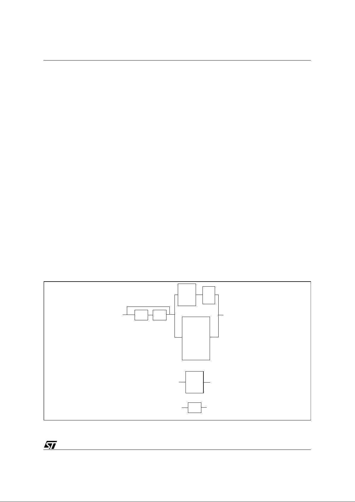
51/89
D950-Core
5.4.4 Program Control Instructions
BREAK Break
BREAKD Break Delayed
CALL Jump to Subroutine
CALLD Call Delayed
CONTINUE Continue
CONTINUED Continue Delayed
JUMP Jump
JUMPD Jump Delayed
LP Low Power
NOP No operation
RESET Reset
RTI Return from interrupt
RTS Return from subroutine
RTSD Return from subroutine Delayed
STOP Stop
SWI Software interrupt
Figure 5.12 Program Contro
l
Note: The condition table is described in Table 4.4
RTI
RTS
RTSD
SWI
NOP
VR02018K
COND
IF
CALL
CALLD
JUMP
JUMPD
addr
A0H
A1H
BREAK
BREAKD
CONTINUE
CONTINUED
LP
RESET
STOP
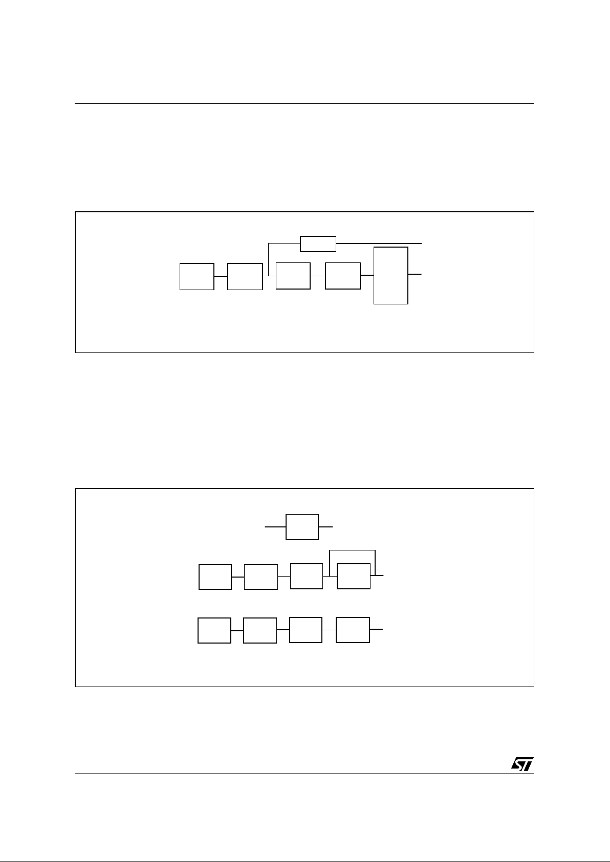
52/89
D950-Core
5.4.5 Conditional Assignment Instruction
LDCC Load conditional: This instruction performs multiple assignment operations,
depending on whether the conditions evaluate to be true or false. For full details of
the instruction, refer to the programming manual.
Figure 5 . 13 Conditiona l Assignment
Note: The condition table is described in Table 4.4
5.4.6 Loop Control Instructions
REP Automatic management of the loop registers (LS, LC, LE and SP)
LSP-- Decrement LSP 2-bit register
LSP++ Increment LSP 2-bit register
Figure 5.14 Loop Control
VR02018L
COND
IF
Ai
=
Aj
Lj
Rj
P
LDCC
value
REP
TIMES
addr
AiH
REP
TIMES
addr
LSP++
LSP--
VR02018M

53/89
D950-Core
5.4.7 Co-processor Instructions
COPD Co-processor Double Move
COPS Co-processor Simple Move
Figure 5.15 Co-processor
Note: Increments allowed, depend on the register used (for COPD instruction only):
AX0:IX0/IX1
AX1:IX2/IX3
AY0:IY0/IY1
AY1:IY2/IY3
*AYn + IYr = COY
*AXm + IXs = COX
COX = *AXm + IXs
COY = *AYn + IYr
COPSxx
*AXm + IXs = COX
COX = *AXm + IXs
COPDxx
,
*AY n + IYr = COY
COY = *AYn + IYr
VR02018N
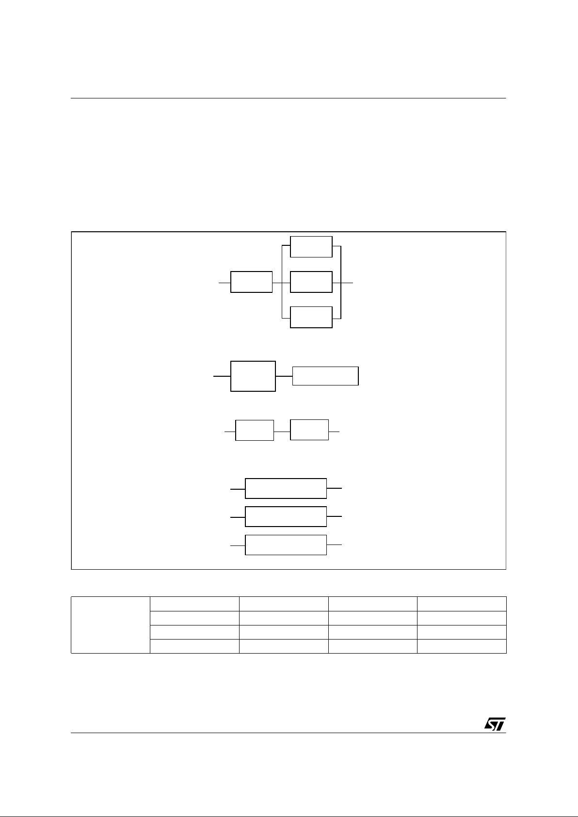
54/89
D950-Core
5.4.8 Stack Instructions
POP Retrieved from Stack
DPOP Double POP
PUSH Saved on the Stack
DPUSH Double PUSH
Figure 5.16 Stack
Note: All references to SP are tak en by the assembler to be SPX.I
Register Pair
0:IX0,IY0 4:L1,L0 8:A0H,A0L 12:BSC/PSC,LC
1:IX1,IY1 5:R0,R0 8:A1H,A1L 13:AOE/A1E,LE
2:IX2,IY2 6:AX0,AY0 9:PH,PL 14:BX,BY
3:IX3,IY3 7:AX1,AY1 10 :CCR,LS 15:MX,MY
POP
PUSH
reg
addr. X
addr. Y
value
DPUSH
reg 1, reg 2
DPOP
SP = SP + IX3
reg = *(SP + IXs)
*(SP + IXs) = reg
55/89
D950-Core
5.5 Instructi o n Cycle and Word Count
Table 5.1 Instruction Cycle and Word Count
Instruction Group / Subgroup Words Cycles
Assignment indirect single 1 1
Assignment indirect double 1 1
Assignment direct 2 2
Assignment indirect indexed 1 2
Assignment immediate short 1 1
Assignment immediate long 2 2
Assignment register to register 1 1
Assignment register / PRAM 1 4
ALU 1-word operand 1 1
ALU 2-word operand 1 1
ALU 3-word operand 1 1
MULT 1 1
DMULT 1 2
ALU Multiplication 1 1
SQR 1 1
Bit Manipulation 2 2
Program Control Non Delayed 1 2 or 3
Program Control Delayed 1 1 or 2
Conditional Assignment 1 1
LDCC 1 2
REPEAT (single) < 512 1 1
REPEAT (sing le ) >
512 2 2
REPEAT (bloc k) < 512 2 2
REPEAT (bloc k) >
512 2 or 3 2 or 3
COPD 1 1
COPS 1 1
PUSH / POP register 1 1
DPUSH / DPOP register 1 1
PUSH / POP direct address 2 3
DPUSH / DPOP direct address 2 3
PUSH immediate value 2 3
DPUSH immediate value 2 3
INC SP 1 1
Register / Stack indirect indexed 1 2
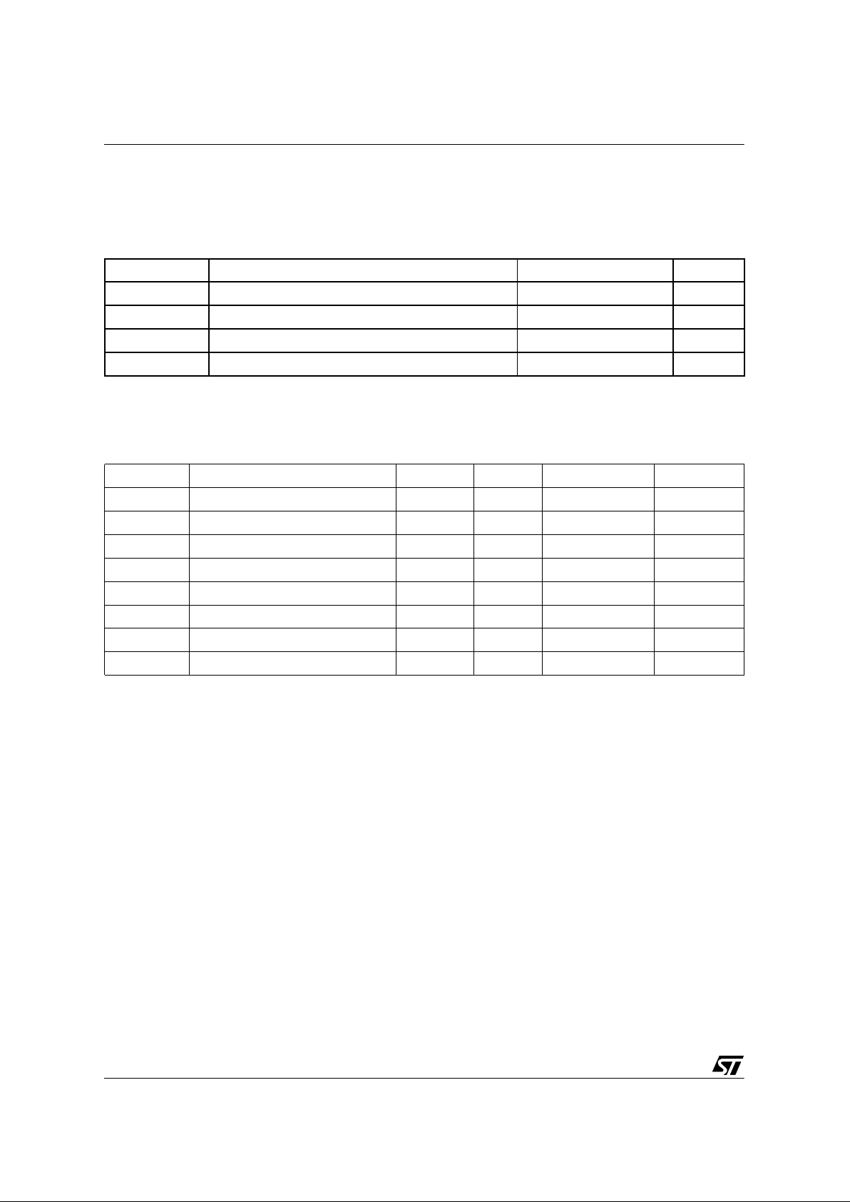
56/89
D950-Core
6 ELECTRI CA L SP EC IF IC AT IO NS
6.1 DC ABSOLUTE MAXIMUM RATINGS
6.2 DC ELECTRICAL CHARACTERISTICS (core level)
Junction temperature : -40°C to +125°C
Symbol Parameter Value Unit
VDD Power Supply Voltage -0.3 / 3.9 V
VIN Input Voltage -0.3 / 3.9 V
T
j
Operating Junction Temperature Range -40 / +125 °C
TSTG Storage Temperature Range -55 / +150 °C
Symbol Parameter Min Typ Max Unit
VDD Power supply 2.7 3.3 3.6 V
VIL Input low level -0.3 V
VIH Input high level V
DD
+ 0.3 V
VOL O utput low lev el I
OL
= 0 0.2 V
VOH Output high level I
OH
= 0 VDD- 0.2 V
IDD Operating current 0.6 mA/MIPS
ILP Low Power current 0.1 mA/MHz
ISTOP Stop current 10 µA
7

57/89
D950-Core
6.3 AC CHARACTERISTICS
Conditions : VDD= 2.7V - 3.6V, Junction temperature : -40°C to +125°C
6.3.1 Bus AC Electrical Characterstics (for X, Y and I buses)
Figure 6.1 Bus AC Electrical Characterstics (for X, Y and I buses)
Note: C_load = 3 pF for all outputs
Num Parameter Min Typ Max. Un it
T0 CLK IN High to INCYCLE High 2.3 ns
T1 INCYCLE High to BS Low/High 0 ns
T2 INCYCLE HiGH to
RD/WR Lo T/4 ns
T2
1
INCYCLE HiGH to RD/WR High 0
T3 INCYCLE High to Address Valid I 1.0 ns
XY 2.3 ns
T4 DATA_IN Setup to
RD High I 1.0 ns
XY 1.5 ns
T5 DATA_IN Hold from
RD High 0 ns
T6
WR Low to DATA_OUT Valid 1.5 ns
T7
WR Low to DATA_OUT Lo-Z 1.0 ns
T8
WR High to DATA_OUT invalid 0 ns
T9
WR High to DATA_OUT Hi-Z 0 ns
VR01939A
BS
RD, WR
2
ADDRESS
3
DATA_IN
DATA_OUT
54
68
7
9
2
1
INCYCLE
CLKIN
0
T
1
2
3
7

58/89
D950-Core
6.3.2 Control I/O Electrical Characteristics
Figure 6.2 Control I/O Electrical Ch aract eristics
Note: C_load = 3 pF for all outputs
CONTROL In/Out are those defined in pin description tables
2.6 and 2.7.
Num Parameter M in Typ Max . Unit
T10 INCYCLE High to CONTROL out valid 2.5 ns
T11 CONTROL In Setup to INCYCLE High 2 ns
T12 CONTROL In Hold from INCYCLE High 0 ns
T13
IT pulse min. duration 3 ns
T14 INCYCLE High to BSU_CLK High 0 ns
T15 DTACK
setup to CLKIN low -1.4 ns
VR01939B
CLKIN
CONTRO L O ut
CONTROL In
11
12
HOLDACK, EOI
13
IT
10
INCYCLE
BSU_CLK
14
DT ACK
15
10
7
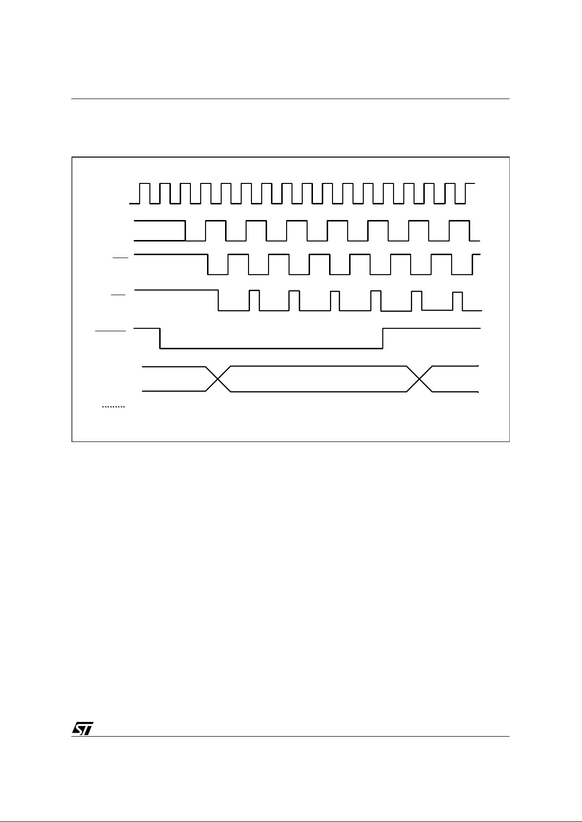
59/89
D950-Core
6.3.3 Hardware Reset
Figure 6.3 Hardware Reset
CLKIN
INCYCLE
IA
XX
IBS
IRD
RESET
0000
XXXX
VR02019G
: Hi - Z
7

60/89
D950-Core
6.3.4 Wait States
Figure 6.4 Write X-bus with 1 Wait-state
CLKIN
VR02005E
INCYCLE
ID
IA
IBS
IRD
XRD
XWR
XA
DTACK
n - 1 nn + 1
In - 1
In
XD
D - Out
XBS
: Hi - Z

61/89
D950-Core
Figure 6.5 Read X-bus with 1 Wait-st ate
CLKIN
VR02005F
INCYCLE
ID
IA
IBS
IRD
XRD
XWR
XA
DTACK
n
In
XD
D - In
XBS
: Hi - Z

62/89
D950-Core
6.3.5 Interrupt
Figure 6.6 Start of Interrupt
Figure 6.7 Ret urn fro m I nterrupt
CLKIN
VR02005C
INCYCLE
IT
IA
ID
: Hi - Z
ITACK
n - 1 n IT
YD
IT
CLKIN
VR02019A
INCYCLE
EOI
IA
ID
Execute
Instruction
: Hi - Z
RTI

63/89
D950-Core
6.3.6 HOLD
Figure 6.8 HOLD (1)
CLKIN
VR02005D
INCYCLE
ID
IA
HOLD
HOLDA CK
IBS
IRD
XBS
XWR
XA
XD
: Hi - Z
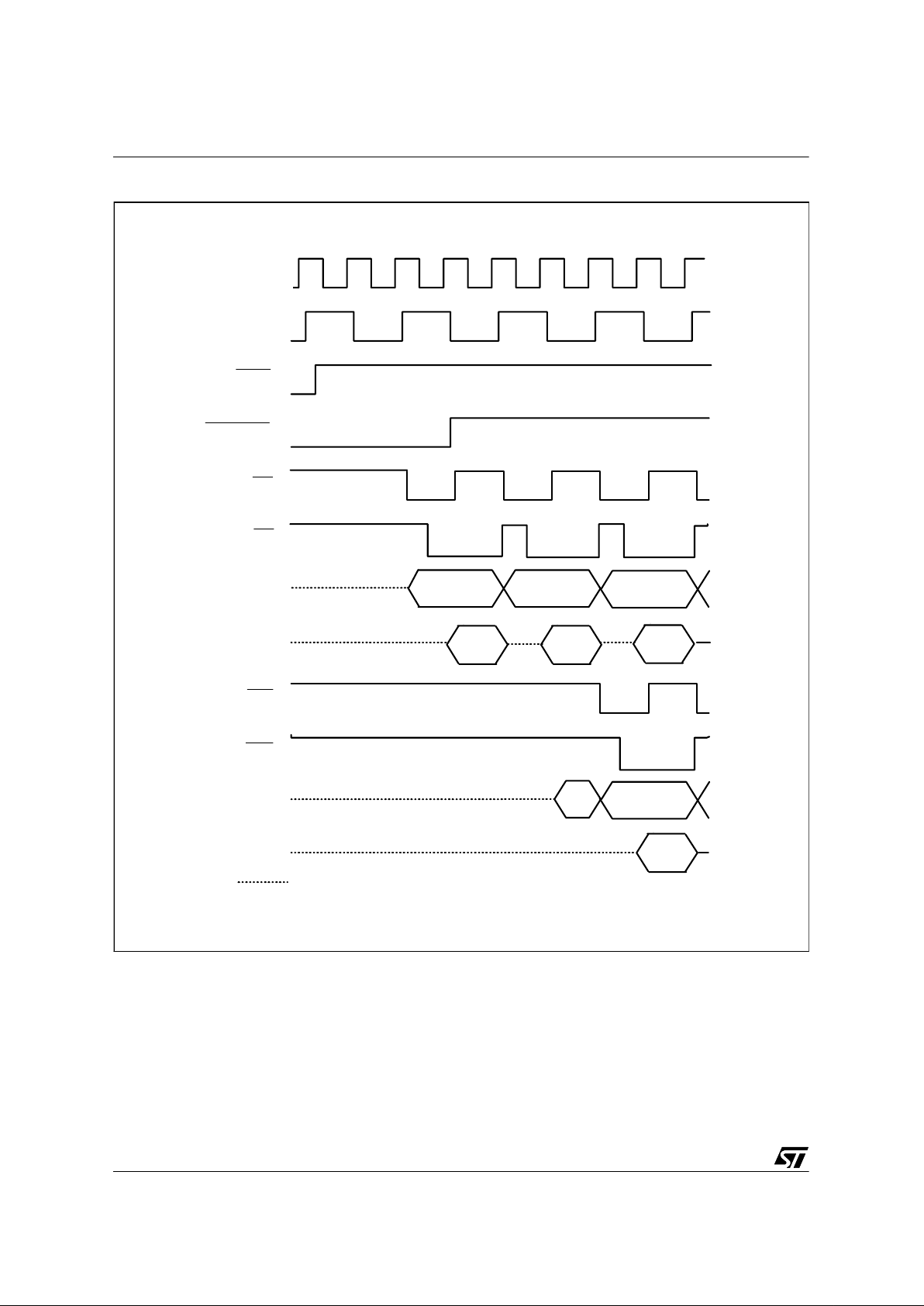
64/89
D950-Core
Figure 6.9 HOLD (2)
CLKIN
VR02005B
INCYCLE
ID
IA
HOLD
HOLDACK
IBS
IRD
XBS
XWR
XA
XD
: Hi - Z

65/89
D950-Core
6.3.7 JUMP on Port Condition
CLKIN
VR02019
INCY CLE
PORT In
ID
IA
nn + 1
n + 2
a_br
a_br + 1
In
In+1
In+2 I_br
(Level Sensitive)
PORT Bit
(Internal)
(Edge Se nsitive )
PORT In
PORT Bit
(Internal)
OPERA TION
Fetch Jump
Decode Jump
Execute Jum p
I_br+1

66/89
D950-Core
7 ANNEX - HARDWARE PERIPHERAL LIBRARY
Specifications for peripheral functions designed for integration with the D 950- Core, are given
in this chapter. An example of an AS-DSP built around the D950-Core and associated
peripherals, is given at the beginning of this data sheet. Other peripherals are available.
Contact your local marketing support for additional information.
The peripherals detailed in this section are:
• Co-processor
• Bus Switch Unit (BSU)
• Interrupt controller
• DMA controller.
7.1 CO-PROCESSOR
Dedicated co-processors can be designed by SGS-Thomson, by custom er request.
The D950-Core instruction set includes two co-processor dedicated one-word instructions,
allowing one (COPS) or two (COPD) parallel data moves between X or Y-memory space and
co-processor registers.
While a co-processor instruction is decoded by the D950-Core, the VC I output is asserted
high, indicating to the co-processor that such an instruction will be executed at the next cycle.
Control and status registers, at least one of each, must be included in the co-processor. This
allows initialization in various operating modes and gives information to the D950-Core on
operations in progress and status.
8
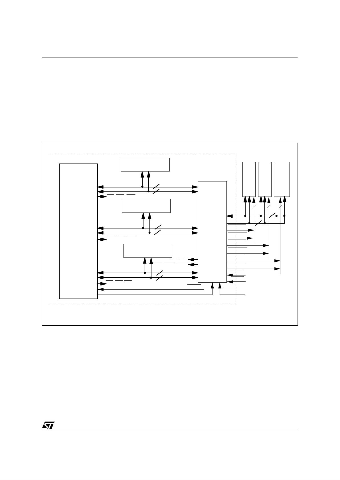
67/89
D950-Core
7.2 BUS SWITCH UNIT (BSU)
7.2.1 Introduction
The D950-Core Bus Switch Unit (BSU) is a multiplexed interface between the D950-Core and
external memory. It enables extension of X, Y and I memories off-chip, allowing multiple
possible configurations for an AS-DSP built around the D950-Core. The figure below shows
the layout of the D950-Core BSU.
Figure 7.1 D950-Core Bus Sw itch Unit
EA
ED
ID
IA
YD
YA
XA
XD
D950-CORE
BUS
SWITCH
UNIT
DTACK
AS-DSP
BSU_CLK
RESET
IRD/XRD/YRD
IWR/XWR/YWR
IBS/XBS/YBS
16
16
16
16
INTE RNAL M EMORIES
& PERIPHERALS
16
16
16
16
P
MEM.
X
MEM.
Y
MEM.
2 22
DT ACKin
EYRD/DS
EYWR/RD
EIRD/DS
EIWR/RD
EXRD/DS
EXWR/RD
VR02020A
INTERNAL MEMORIES
& PERIPHERALS
INTERNAL MEMORIES
& PERIPHERALS
DEID/DEXD/DEYD
IID/IXD/IYD
IDT_EN
8

68/89
D950-Core
7.2.2 I/O interface
In this section, the terms input and output are related to BSU, and the terms internal and
external are related to the AS-DSP.
The BSU I/O interface signals are of two types:
On the D950-Core side:
IA0/IA15 (I address bus) and ID0/ID15 (I data bus) with their associated control
signals:
IRD
(read / input)
IWR
(write / input)
IBS
(bus strobe / input)
XA0/XA15 (X address bus) and XD 0/XD15 (X data bus ) with their associated control
signals:
XRD
(read / input)
XWR
(write /input)
XBS
(bus strobe / input)
YA0/YA15 (Y address bus) and YD0/YD15 (Y data bus) with their associated control
signals:
YRD
(read / input)
YWR
(write / input)
YBS
(bus strobe / input)
DTACK
(data transfer acknowledge / output)
BSU_CLK (clock / input)
On the internal memory side:
IID
(internal I-memory space deselect / output)
IXD
(internal X-memory space deselect / output)
IYD
(internal Y-memory s pace des elec t / output)
8

69/89
D950-Core
On the external side:
EA0/EA15 (external address bus) and ED0/ED15 (external data bus) with their associated control signals
EXRD
/DS (external X-bus read (*) or data strobe (**) / output)
EXWR
/RD (external X-bus write (*) or read/write (**) / output)
EYRD
/DS (external Y-bus read (*) or data strobe (**) / output)
EYWR
/RD (external Y-bus write (*) or read/write (**) / output)
EIRD
/DS (external I-bus read (*) or data strobe (**) / output)
EIWR
/RD (external I-bus write (*) or read/write (**) / output)
DEID
(direct access external I memory enable)
DEXD
(direct access external X memory enable)
DEYD
(direct access external Y memory enable)
Note: (*) INTEL type interface
(**) MOTOROLA type interface
RESET (reset / input)
DTACKin (data transfer acknowledge/input)
7.2.3 Operation
The BSU recognizes a bus cycle when IBS, XBS or YBS is activated. It decodes the address
value to determine if an external memory access is requested on the I, X or Y-bus and
generates the appropriate signals on the external bus side. The BSU can also generate the
DTACK signal only, depending on a control register bit value.
If more than one external memory access is attempted at one instruction cycle, they are
serviced sequentially in the following order: I-bus, X-bus, Y-bus.
If one or more external mem ory accesses are attempted in read mode, the corresponding
internal memory space can be disabled us ing IID
(for I-bus), IXD (for X-bus) or IYD (for Y-bus),
assigned low until the end of the instruction cycle.
Each external access requires one basic instruction clock cy cle (two CLKIN cycles), extended
by, at least, one wait-state (one BSU_CLK cycle). The number of wait-states can be extended,
either by software with the BSU control registers (see Section 7.2.4), or by hardware with the
DTACKin
signal.
During each external memory access and according to the selected interface (INTEL or
MOTOROLA) and bus (X, Y or I), the corresponding external control signals are assigned low
and synchronized to the rising edge of BSU_CLK.
8
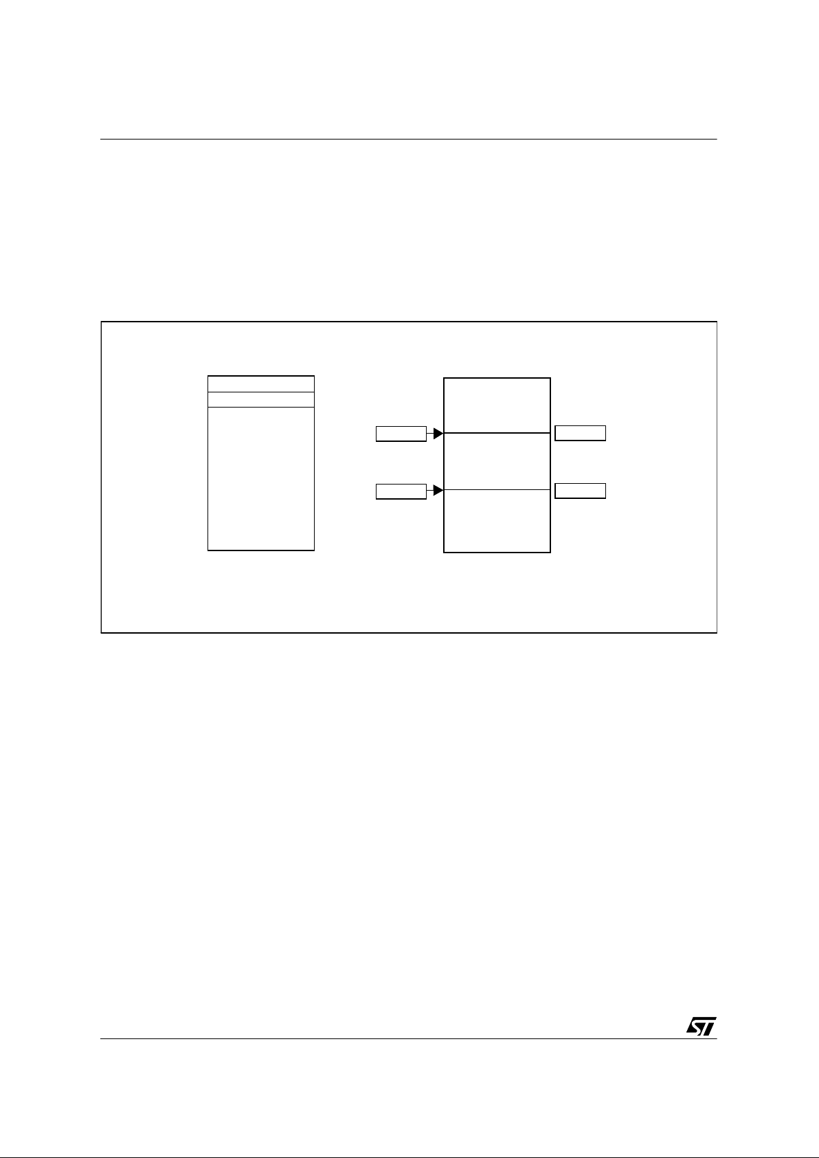
70/89
D950-Core
7.2.4 BSU control registers
The BSU is software controlled by six control registers mapped in the Y-memory space. These
define the type of memory used, internal to external boundary address crossing and software
wait-states count.
There are 2 registers per memory space, making it possible to define 2 sets of boundries and
wait state numbers.
Figure 7.2 Default and User Mapping Examples
The BSU control registers include a reference address on bits 4 to 9, where the internal/
external memory boundary value is stored (see Fig ure 7.2) , and software wait-states count on
bits 0 to 3, allowing up to 16 wait-states.
External addressing is recognized by comparing these address bits for each valid address
from IA, XA and YA, to the reference address contained into the corresponding control
register.
If the address is greater or equal to the reference value, an external access proceeds.
For the following examples, ‘-’ means RESERVED (read: 0, write: don't care)
EXTERNAL
INTERNAL1
64K
63K
62K
INTERNAL0
DEFAULT MAPPING (RESET)
USER MAPPING
(CAN CHANGE BY 1K STEP)
VALUE 1
VALUE 0
VALUE 1
VALUE 0
EXTERNAL
INTERNAL1
INTERNAL0
64K
0
0
8
71/89
D950-Core
XER0/1: X-memory space control registers
After reset, XER0/1 default values are 0x83EF/0x83FF
IM: Intel/ Motorola
0: Motorola type for memories
1: Intel type for memories (def.)
EN_X: Enable for X-space data exchanges
XA15 / XA10 X-memor y s pace map for boundar y on-chi p or off-chip
W3 / W0: Wait state count (1 to 16) for off-chip access (X-mem ory space)
YER0/1: Y-memory space control registers
After reset, YER0/1 default values are 0x83EF/0x83FF
IM: Intel / Motorola
0: Motorola type for memories
1: Intel type for memories (def.)
EN_Y: Enable for Y-space data exchanges
YA15 / YA10: Y-memory space Map for boundary on-chip or off-chip
W3 / W0: Wait state count (1 to 16) for off-chip access (Y-memory space)
IER0/1: Instruction memory control registers
After reset, IER0/1 default values are 0x83EF/0x83FF
IM: Intel / Motorola
0: Motorola type for memories
1: Intel type for memories (def.)
EN_I: Enable for I-space data exchanges
IA15 / IA10: I- m em ory space Map for boundary on-chip or off-chip
W3 / W0: Wait state count (1 to 16) for off-chip access (I-memory space)
1514131211109876543210
IMEN_X----XA15XA14XA13XA12XA11XA10W3W2W1W0
1514131211109876543210
IMEN_Y----YA15YA14YA13YA12YA11YA10W3W2W1W0
1514131211109876543210
IMEN_I----IA15IA14IA13IA12IA11IA10W3W2W1W0
8
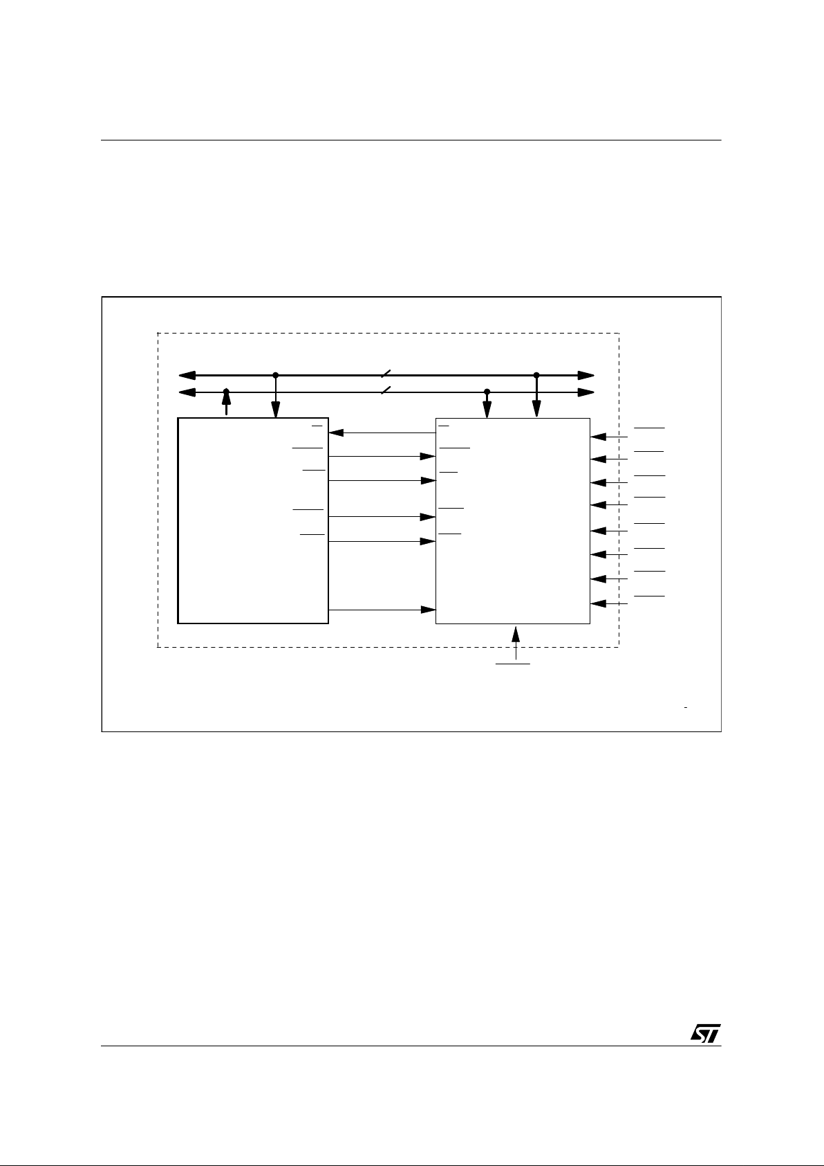
72/89
D950-Core
7.3 INTERRUPT CONTROLLER
7.3.1 Introduction
The D950-Core interrupt controller is a peripheral that manages up to eight interrupt sources.
Figure 7.3 D950-Core Interrupt Controller Peripheral
YD
YA
16
16
D950-CORE
INTERRUPT
CONTROLLER
PERIPHERAL
ITRQ1
IT
ITACK
EOI
YWR
RESET
CLK
INCYCLE
IT
ITACK
YWR
YRD
YRD
EOI
ITRQ0
ITRQ2
ITRQ3
ITRQ4
ITRQ5
ITRQ6
ITRQ7
AS-DSP
VR02020C
8

73/89
D950-Core
7.3.2 I/O interface
In this section, the terms input and output are related to the interrupt controller, and the term
external is related to the AS-DSP.
The interrupt controller I/O interface signals are of two types:
On the D950-Core Side
•IT
(maskable interrupt request / output)
•ITACK
maskable interrupt request acknowledge / input)
•EOI
(end of maskable interrupt routine / input)
• YA0/YA15 (Y address bus) and YD0/YD15 (Y data bus) with their associated
control signals:
YRD
(read / input)
YWR
(write / input)
• CLK clock / input
On the External Side
•ITRQ
(7:0) (8 interrupt requests / inputs)
• RESET
(reset / input)
7.3.3 Interrupt Controller Peripheral Registers
The interrupt controller interface is software controlled by thirteen status/control registers
mapped in the Y-memory space. Status registers are not protected against writing:
IVi: Interrupt Vector Register
One register is associated to each external interrupt.
IVi contains the first address of the interrupt routine associated to each ITRQi
interrupt input
(with 0
<i<7). The register content of the interrupt under service is assigned on the YD-bus
during the cycle following the ITACK
falling edge where CLK=0.
After reset, IVi default value is 0.
IMR: Interrupt Mask Register
Each interrupt ITRQi
can be masked individually when the IMi corresponding bit is set. In this
case, no activity on IT RQi
is taken into account.
ITRQi
can be activated on a low level or on a falling edge, according to associated ISi status.
When associated ISi-bit is reset (def. value), ITRQi
must stay low for one period.
After reset, IMR default value is 0x5555.
8

74/89
D950-Core
For the following examples, ‘-’ means RESERVED (read: 0, write: don't care)
IMi: Interrupt Mask
0: Interrupt i is not masked
1: Interrupt i is masked (def.)
ISi: Sensitivity
0: ITRQi
is active on a low level (def.)
1: ITRQi
is active on a falling edge
IPR: Interrupt Priority Register
IPR contains the priority level of each ITRQi
interrupt input.
Interrupt priority level is a 2-bi t value, so can be 0,1,2 or 3 (0 lowest priority, 3 hi ghest pri ority).
When two ITRQi
of same priority level are requested during the same cycle, the first
acknowledged interrupt is the interrupt corresponding to the lowest numberical value.
After reset, IPR default value is 0.
IPi: Interrupt Priority level (0, 1, 2 or 3) (def. 0)
ICR: Interrupt Con tr ol Re gister
ICR displays the current priority level and up to four stacked priority levels.
The current priority level is coded using 3 bits but only five different values are available:
Note: The D950-Core interrupts (SWI, RESET) are priority level 4 (highest level).
An interrupt request is acknowledged when its priority level is strictly higher than the current
priority level. In this case, the current priority level becomes the interrupt priority level and the
previous current priority level is pushed onto the stack and displayed as SPL1.
15 14 13 12 11 10 9 8 7 6 5 4 3 2 1 0
IS7IM7IS6IM6IS5IM5IS4IM4IS3IM3IS2IM2IS1IM1IS0IM0
15 - 14 13 - 12 11 - 10 9 - 8 7 - 6 5 - 4 3 - 2 1 - 0
IP7 IP6 IP5 IP4 IP3 IP2 IP1 IP0
PRIORITY LEVEL CODING ACCEPTABLE IT LEVEL PRIORITY
- 1 111 0,1,2,3
0 000 1,2, 3
1 001 2,3
2 010 3
3 011
Reserved 100 - 110
8
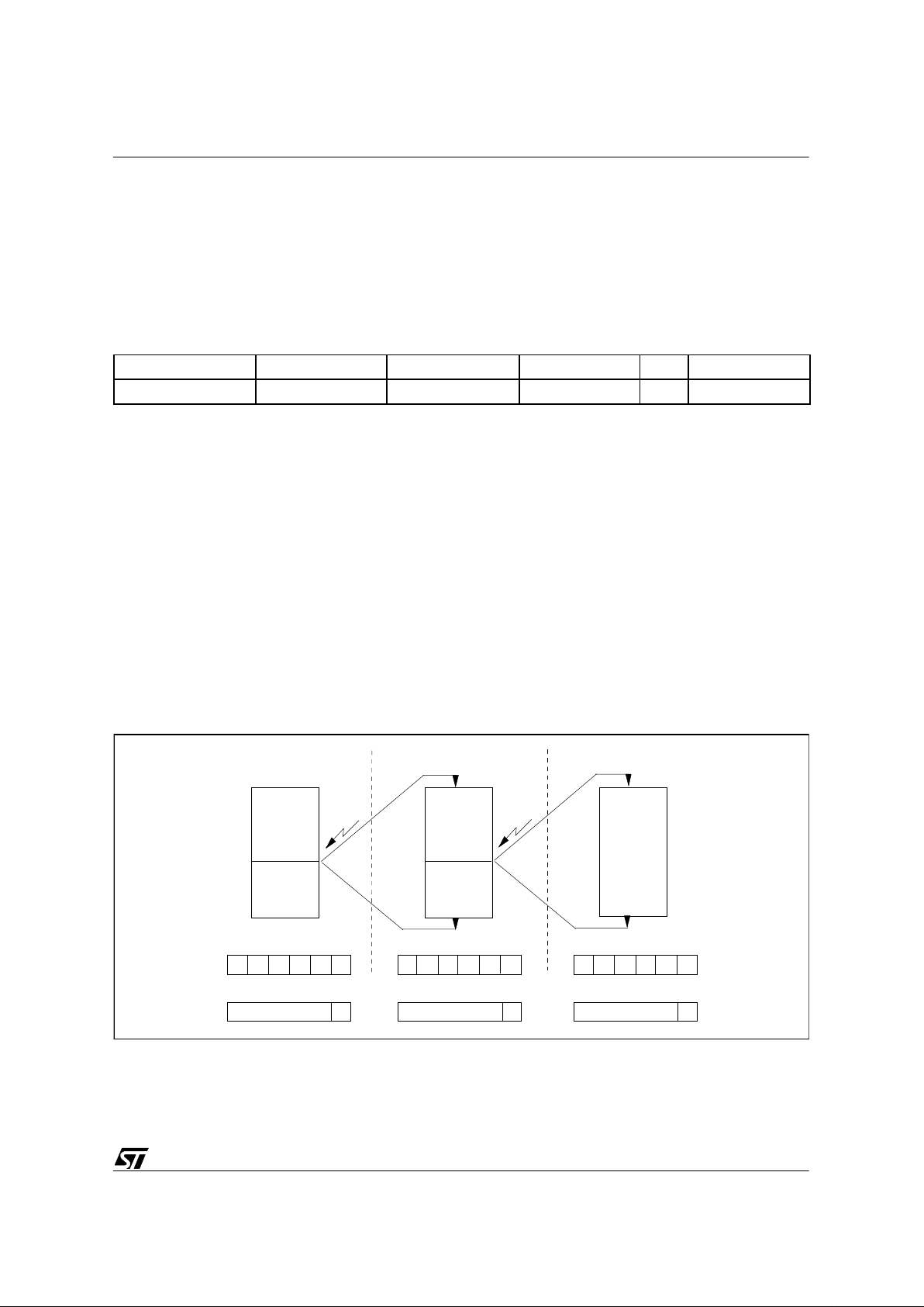
75/89
D950-Core
The process is repeated over a range of four interrupt requests and the four previous current
priority levels are displayed as SPL1, SPL2, SPL3 and SPL4. If less than four interrupts are
pushed onto the stack, the unused Stack Priority Level words are reset to ‘000’.
At the end of the interrupt routine, the priority levels are popped from the stack.
If the SPLi values are directly written, the register content is not more significant but the
interrupt routine procedure is not affected. The only way to affect this is to reset the AS-DSP.
After reset, ICR default value is 0x000B.
SPL4: 3-bit 4th stacked priority level
SPL3: 3-bit 3rd stacked priority level
SPL2: 3-bit 2nd stacked priority level
SPL1: 3-bit 1st stacked priority level
ES: Empty Stack flag
0: Stack is used
1: Stack is not used (def.)
CPL: Current Priority level (-1, 0, 1, 2 or 3) (def. 011)
Note:After reset, no interrupt request from interrupt controller is acknowledged.
‘-’ means RESERVED (read: 0, write: don't care)
Figure 7.4 ICR and ISPR Operation
15 - 14 - 13 12 - 11 - 10 9 - 8 - 7 6 - 5 - 4 3 2 - 1 - 0
SPL4 SPL3 SPL2 SPL1 ES CPL
INTERRUPT LEVEL 2
PROGRAM
PROGRAM
IT2
PROGRAM
IT3
IT2
IT3
INTERRUPT LEVEL 3
XXXX1
-1
SPL4 SPL3 SPL2 SPL1 ES CPL
XXX-10
2
SPL4 SPL3 SPL2 SPL1 ES CPL
XX-120
3
0 1 2
ISP ISPISP
ICR
ISPR
VR02020D
8

76/89
D950-Core
ISPR Interrupt Stack Pointer Register
ISPR contains the number of stacked priority levels. If the ISP R value is directly written, the
SPLi/CPL values are modified. So the ICR register content is no longer significant but the
interrupt routine procedure is not affected. After reset, ISPR default value is 0.
ISPR: Number of stacked priority levels (0, 1, 2 or 3)
Note:’-’ is RESERVED (read: 0, write: don't care)
ISR Interrupt Status Register
ISR contains the eight interrupt pending bits, each being associated to one ITRQi
interrupt
inpu t.
IPEi-bit is set when the interrupt request is recorded and is reset when the interrupt request is
acknowledged (ITACK
falling edge).
An interrupt request will not be acknowledged when IPEi-bit is reset by direct register write.
An interrupt request will be generated whatever the state of ITRQi
when IPEi-bit is set by a
direct register write.
When only some pending interrupt r equests need to be acknowledged, the IPEi bits of the
other ITRQi
interrupt inputs must be reset.
When none of the pending interrupt requests need to be acknowledged, the IPE-bit of CCR
register must be first reset and ISR must be reset.
When IMi-bit is set, the corresponding IPEi-bit is reset. After reset, ISR default va lue is 0.
IPEi: Interrupt Pending bit
0: Reset when interrupt request is acknowledged (def.)
1: Set when interrupt request is recorded
Note:‘-’ is RESERVED (read: 0, write: don't care)
15 14 13 1 2 11 10 9 8 7 6 5 4 3 2 - 1 - 0
------------- ISPR
1514131211109876543210
--------IPE7IPE6IPE5IPE4IPE3IPE2IPE1IPE0
8

77/89
D950-Core
7.4 DMA CONTROLLER
7.4.1 Introduction
The D950-Core DMA controller manages data transfer between AS-DSP memories and
external peripherals, without using AS-DSP capabilities.
Figure 7.5 D950-Core DMA Controller Peripheral
YD
YA
16
16
D950-CORE
INTERRUPT
CONTROLLER
PERIPHERAL
RESET
AS-DSP
HOLD
HOLDACK
INCYCLE
DMA CONTROLLER PERIPHERAL
DMARQ0
DMARQ1
DMARQ2
DMARQ3
DMACK0
DMACK1
DMACK2
DMACK3
DTACK
DIP_ENA
16 16 16 16
IA ID XA XD
IRD
IWR
IBS
XRD
XWR
XBS
YRD
YWR
YBS
DIT0 DIT1 DIT2 DIT3 DIT_AND
3
3
3
VR02020E
CLK
DMA_CLK
8

78/89
D950-Core
7.4.2 I/O interface
The terms input and output are re lated to the DMA controller, external is re lated to the ASDSP.
Referring to the D950-Core pin description, the interrupt controller I/O interface signals are of
different types:
On the D950-Core Side
•HOLD
(hold request / output)
• HOLDACK
(hold acknowledge / input)
• CLK (clock / input)
• INCYCLE (clock / input)
On the Internal Memory Side
• XA0/XA15 (Y address bus) with associated control signals (output):
XRD
(read / output)
XWR
(write / output)
XBS
(bus strobe / output)
• YA0/YA15 (Y address bus) and YD0/YD15 (Y data bus) with their associated
control signals (clock / input):
YRD
(read / input/output)
YWR
(write / input/output)
YBS
(bus strobe / output)
• IA0/IA15 (I address bus) with associated control signals (output):
IRD
(read / output)
IWR
(write / output)
IBS
(bus strobe / output)
On the Interrupt Controller Side
• DIT(3:0)
(interrupt request / output)
•DIT_AND
(common interrupt request / output)
On the External Side
•DMARQ(3:0)
(request / one input per channel)
• DMACK(3:0)
(acknowledge / one output per channel)
• DIP_ENA (DITi output enable / input)
• RESET
(reset / input)
•DTACK
(cycle extension / input),
8

79/89
D950-Core
7.4.3 Operation
The DMA controller interface contains four independent channels allowing data transfer on Imemory space and simultaneous data transfer on X and Y- memory spaces. When requests
occur at the same time on different channels, to transfer data on the same bus, the requests
are concatenated to be acknowledged during the same transfer, according to the following
fixed priority (see table):
The DMA transfer is based on a DSP cycle stealing operation:
• The DMA controller generates a ‘hold request’ to the AS-DSP.
• The AS-DSP sends back a ‘hold acknowledge’ to the DMA controller and
enters the hold state (bus released).
• The DMA controller, manages the transfer and enters its idle state at the end of
the transfer, until reception of a new DMA request. The ‘hold request’ signal is
removed.
The data transfer duration is n+2 cycles, split into:
• One cycle inserted at the beginning of the transfer when bus controls are
released by the D950-Core, n cycles for the number of data words to be transferred.
• Another cycle is inserted at the end of the transfer when bus controls are
released by the DMA controller.
Single or block data can be tr ansferred. The ‘ DMA request’ si gnal is w ell adapted to s uch data
transfers by being either edge (single) or l evel (block) sensit ive. Nevertheless, data bloc ks can
be transferred one data at time using an edge sensitive request signal.
A double buffering mechanism is available to deal with data blocks requiring the allocation of
2N addresses for the transfer of a N data block.
An interrupt can be used to warn AS-DSP that a predefined number of data have been
transferred and are ready to be processed. Interrupt requests are sent from the DMA controller
to the interrupt controller. The selected channels must be edge sensitive and the user has to
define the proper priority.
There are two ways to connect the DMA and the interrupt controllers, depending on the state
on the DIP_ENA static pin:
• DIP_ENA = 0, there are enough available interrupt sources in the interrupt
controller: connect each DMA channel interrupt request (DITi
, active on falling
Table 7.1 DMA Controller Interface Priority Levels
Priority Channel Level
0 0 Highest
11
22
3 3 Lowest
8

80/89
D950-Core
edge) to an interrupt input (ITRQi).
• DIP_ENA = 1, the number of available interrupt sources in the interrupt
controller is low: Connect the logical AND of the D ITi
signals (DIT_AND) to a
single interrupt input (ITRQi), the interrupt pending bits (DIPi) of the DAIC
register distinguish the which of the four possible interrupt sources caused the
interrupt. (see 7.4.4).
7.4.4 DMA Peripheral Registers
Address Registers
Two 16-bit registers (unsigned) are dedicated per channel for transfer address:
• DIA: initial address. This register contains the initial address of the selected
address bus (see DBC-bit of DGC).
• DCA: current address. This register contains the value to be transferred to the
selected address bus (see DBC-bit of DGC) during the next transfer. The
different DCA values are:
Note: See DAIC register for DAI and DLA definitions
Counting Registers
Two 16-bit registers (unsigned) per channel are dedicated for transfer count.
For a transfer of a N data block, DIC and DCC registers have to be loaded with N-1.
When DCC content is 0 (valid transfer count), it is loaded with DIC content for the next transfer.
• DIC: initial count. This register contains the total number of transfers of the
entire block
• DCC: current count. This register contains the remaining number of transfers
to be done to fill the entire block. It is decremented after each transfer. The
DCC values are:
RESET DAI DLA DCC = 0 DCA(n+1)
1XX X 0
0 0 X X DCA(n)
0 1 0 X DCA(n) + 1
0 1 1 0 DCA(n) + 1
011 1 DIA
RESET DCC = 0 DCA(n+1)
1X0
0 0 DCA(n) - 1
01DIC
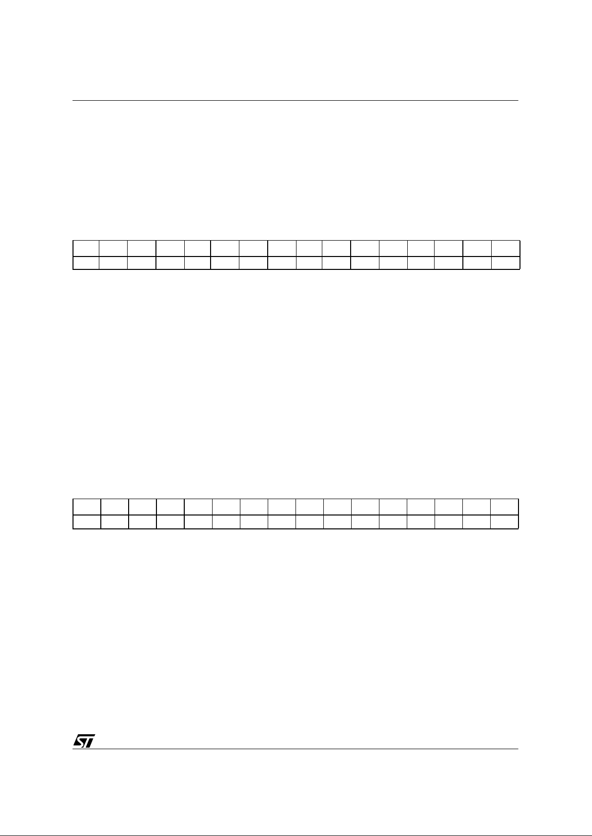
81/89
D950-Core
Control Registers
Three 16-bit control registers are dedicated to the DMA controller interface. These are the
general control register, the address interrupt control register and the Mask sensitivity control
register. They are detailed as follows:
DGC: General control register
Three bits are dedicated for each DMA channel (bits 0 to 2 to channel 0, bits 4 to 6 to channel
1, bits 8 to 10 to channel 2, bits 12 to 14 to channel 3). After reset, DGC default value is 0.
DBC1/DBC0: Bus choice for data transfer
0 : X-bus (def.)
01: Y-bus
10: I-bus
11: reserved
DRWi: Data transfer direction
0: Write access (def.)
1: Read access
DAIC: Address/Interrupt control register
Four bits are dedicated for each DM A channel (bits 0 to 3 to channel 0, bits 4 to 7 to channel
1, bits 8 to 11 to channel 2, bits 12 to 15 to channel 3). After reset, DAIC default value is 0.
DAIi: Address increment
0: DCAi content unchanged (def.)
1: DCAi content modified according to DLAi state
DLAi: Load address
0: DCAi content incremented after each data transfer (def.)
1: DCAi content loaded with DIA content if DCCi value is 0 or DCAi content
incremented if DCCi value not equal to 0
DIPi: Interrupt pending
0: No pending interrupt on channel i (def.)
1: Pending interrupt on channel i (enabled if DIP_ENA input is high)
15 14 13 12 11 10 9 8 7 6 5 4 3 2 1 0
- DRW3 DBC1 DBC0 - DRW2 DBC1 DBC0 - DRW1 DBC1 DBC0 - DRW0 DBC1 DBC0
1514131211109876543210
DAI3 DLA3 DIP3 DIE3 DAI2 DLA2 DIP2 DIE2 DAI1 DLA1 DIP1 DIE1 DAI0 DLA0 DIP0 DIE0

82/89
D950-Core
DIEi: Enable Interrupt
0: Interrupt request output associated to channel i is masked (def.)
1: Interrupt request output associated to channel i is not masked
DMS: Mask Sensitivity control register
Two bits are dedicated to each DMA channel (bits 0 and 1 to channel 0, bits 4 and 5 to channel
1, bits 8 and 9 to channel 2, bits 12 and 13 to channel 3). After reset, DMS default value is
0x3333.
DSEi: DMA Sensitivity
0: Low level
1: Falling edge (def.)
DMKi: DMA Mask
0: DMA channel not masked
1: DMA channel masked (def.)
15 14 13 12 11 10 9 8 7 6 5 4 3 2 1 0
- - DSE3 DMK3 - - DSE2 DMK2 - - DSE1 DMK1 - - DSE0 DMK0
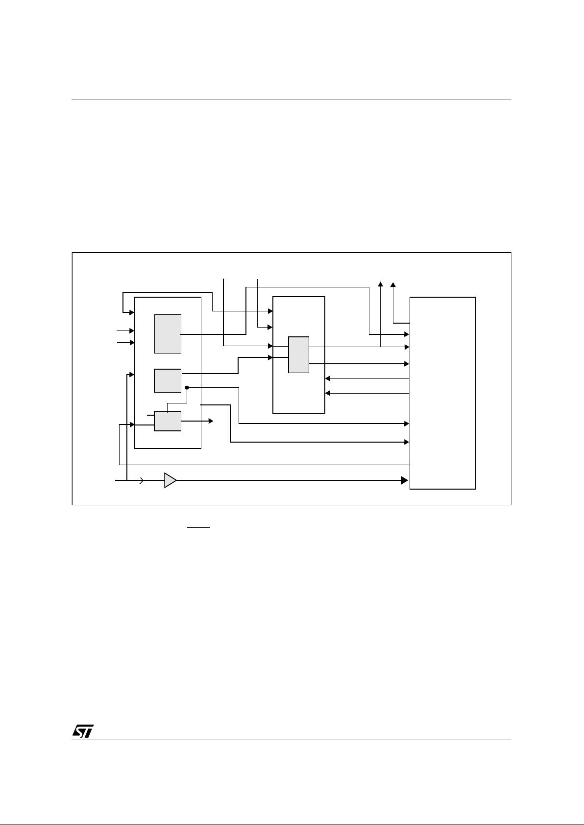
83/89
D950-Core
7.5 Emulation and Test Unit (EMU)
7.5.1 Introduction
The D950-Core EMU is a peripheral which performs functions dedicated to emulation and test
through the external IEEE 1149.1 JTAG interface.
The emulation and test operations are controlled by an off-core Test Access Port (TAP) and
an off-core emulator by means of dedicated control I/Os.
Figure 7.6 D950-Core Emulation and Test
Emulation mode can entered in two ways:
• Asser ting ER Q
input pin low.
• Meeting a valid breakpoint condition or executing an instruction in single step
mode.
Most of D950-Core instructions can be executed in emulation mode, including arithmetic/logic,
JUMP/CALL and MOVE. These instructions are used to display the processor status
(memories and registers) and restore the context.
Exiting the emulation mode is controlled by the PC-board emulator through the JTAG
interface.
TAP
CORE
Instr.
Reg.
out.
mux
EMU
TAP
D950
NTRST
TMS
TCK
TDI
TDO
NERQ
AI,X,YEBP
TI_CORE
TO_CORE
UPDATE_DR
BUS + CTRL
FNOP,INCYCLE,LPACK
HALTACK,MCI
HALT
SNAP
IDLE
CLK_EMU
TEST_D950
EMU_D950
TEST
EMI
84/89
D950-Core
The Emulation resources (see Figure 7.7) include:
• Four Breakpoint registers (BP0, BP1, BP2, BP3) which can be affected by
Program or Data memory.
• Breakpoint counter (BPC).
• Program Counter Trace Buffer (PCB) able to store the address of the 6 last
executed instructions.
• Three control registers for Breakpoint condition programming.
• Control logic for instruction execution through the PC-board emulator control.
Figure 7.7 D950-Core Emulation Block Diagram
The emulation and TAP controller interfaces (see Table 2.7 and Table 2.8) include pins of
different types:
• Scan control (TDI, TDO, TCK).
• TAP instructions
• TAP controller states (UPDATE).
• Emulation control (ERQ, IDLE, SNAP, HALTACK, AIEBP, AXEBP, AYEBP).
BP registers
Comparators
XA / YA
XD / YD
IA
Control
Registers
Control
Logic
PC trace
ERQ, IDLE, SNAP
RD/WR
PCU
TAP
IA
85/89
D950-Core
7.5.2 Registers
There are two types of registers for the EMU, data registers, and control and status registers.
They are mapped in the Y-memory space.
Data Registers
BP0, BP1, BP2, BP3: Breakpoint registers
0, 1, 2, 3 values. 16-bit breakpoint registers allowing breakpoints.
BPC: Breakpoint Counter register. This 16-bit register is initialized by a load instruction and
decremented each time a valid condition is met on a count enabled breakpoint. Breakpoints
with and without a count condition can be set simultaneously. After reset, BPC is not initialized.
PCB: Program Counter Trace Buffer register allows the user to keep trace of the PC value for
the six last executed instructions. PCB stores one address value per instruction, whatever the
instruction type (single cycle, single word, multiple cycles, multiple words)
Control and Status Registers
Three breakpoint control registers allow simple or multiple breakpoints (conditional or not) to
be set and counting breakpoint events to be enabled..
Breakpoint Register Breakpoint Location Bus
BP3 Program memory address IA or YD
BP2 or Data memory data IA or XD
BP1 Data memory XA or
BP0 Address YA
86/89
D950-Core
8 APPENDIX
8.1 MEMORY MAPPING (Y-mem ory space)
8.1.1 General mapping
Miscellaneous 006F
0060
Bus Switch Unit 005F
0050
DMA CONTROLLER 004F
0030
IT Controller 002F
0020
DSP Core 001F
0000
9

87/89
D950-Core
8.1.2 Registers Related to the D950-CORE
8.1.3 Registers related to the interrupt controller
Register
Address
Register
Name
Function Location
0x0000 BX Modulo base address for
X-memory space
ACU
0x0001 MX Modulo max imum address for
X-memory space
ACU
0x0002 BY Modulo base address for
Y-memory space
ACU
0x0003 MY Modulo max imum address for
Y-memory space
ACU
0x0004 POR Port Output Register PORT
0x0005 PIR Port Input Register PORT
0x0006 PCDR Port Control Direction Register P ORT
0x0007 PCSR Port Control Sensitivity Register PORT
0x0008
to
0x001F
Reserved for test and emulation
0x0062 PPR Program Page Register Peripherals
Register
Address
Register
Name
Function Location
0x0020 IV0 Interrupt Vector 0 address IT Controller
0x0021 IV1 Interrupt Vector 1 address IT Controller
0x0022 IV2 Interrupt Vector 2 address IT Controller
0x0023 IV3 Interrupt Vector 3 address IT Controller
0x0024 IV4 Interrupt Vector 4 address IT Controller
0x0025 IV5 Interrupt Vector 5 address IT Controller
0x0026 IV6 Interrupt Vector 6 address IT Controller
0x0027 IV7 Interrupt Vector 7 address IT Controller
0x0028 ICR Interrupt Control Register IT Controller
0x0029 IMR Interrupt Mask / Sensitivity Register IT Controller
0x002A IPR Interrupt Priority Register IT Controller
0x002B ISPR Interrupt Stack Pointer Register IT Controller
0x002C ISR Interrupt Stat us Register IT Controller
9

88/89
D950-Core
8.1.4 Registers related to the DMA controller
8.1.5 Registers related to the Bus Switch Unit
Register
Address
Register
Name
Function Location
0x0030 DIA0 DMA channel 0 initial address DMA controller
0x0031 DIA1 DMA channel 1 initial address DMA controller
0x0032 DIA2 DMA channel 2 initial address DMA controller
0x0033 DIA3 DMA channel 3 initial address DMA controller
0x0034 DCA0 DMA channel 0 current address DMA controller
0x0035 DCA1 DMA channel 1 current address DMA controller
0x0036 DCA2 DMA channel 2 current address DMA controller
0x0037 DCA3 DMA channel 3 current address DMA controller
0x0038 DIC0 DMA channel 0 initial count DMA controller
0x0039 DIC1 DMA channel 1 initial count DMA controller
0x003A DIC2 DMA channel 2 initial count DMA controller
0x003B DIC3 DMA channel 3 initial count DMA controller
0x003C DCC0 DMA channel 0 current count DMA controller
0x003D DCC1 DMA channel 1 current count DMA controller
0x003E DCC2 DMA channel 2 current count DMA controller
0x003F DCC3 DMA channel 3 current count DMA controller
0x0040 DGC DMA General Control DMA controller
0x0041 DMS DMA Mask Sensitivity DMA controller
0x0042 DAIC DMA Address / Interrupt Control DMA controller
Register
Address
Register
Name
Function Location
0x0050 IER0 External I-bus control register 0 BSU
0x0051 XER0 External X-bus control register 0 BSU
0x0052 YER0 External Y-bus control register 0 BSU
0x0053 IER1 External I-bus control register 1 BSU
0x0054 XER1 External X-bus control register 1 BSU
0x0055 YER1 External Y-bus control register 1 BSU
9

89/89
Information furnished is believed to be accurate and reliable. However, SGS-THOMSON Microelectronics assumes no responsibility for the
consequences of use of such information nor for any inf ringe m ent of pa t ents or other ri ghts of thir d p arties which m ay resu l t from its use. No
license is granted by implication or otherwise under any patent or patent rights of SGS-THOMSON Microelectronics. Specifications
mentione d in this publi cation are sub ject to chang e without notice. This public ation superse des and replaces all informa tion previous ly
supplied. SGS-TH OMSON M icroele ctronic s produc ts are not authoriz ed for us e as cri tical compo nents i n life su pport dev ices or s ystems
without th e express wr i tten approval of SGS-THOMSON Microel ectronics .
1997 SGS-THOMSON Microelectroni cs - All rig hts reserved.
SGS-THOMSON Microelectronics Group of Companies
Austra l i a - B razil - Canada - China - France - Germany - Hong Ko ng - Italy - Jap an - K o rea - Malaysia - Malta - Morocco
The Nether l ands - Singapore - Spain - Sweden - Swi tzerland - T ai wan - Thaila nd - United Kingdom - U. S.A.
10
 Loading...