


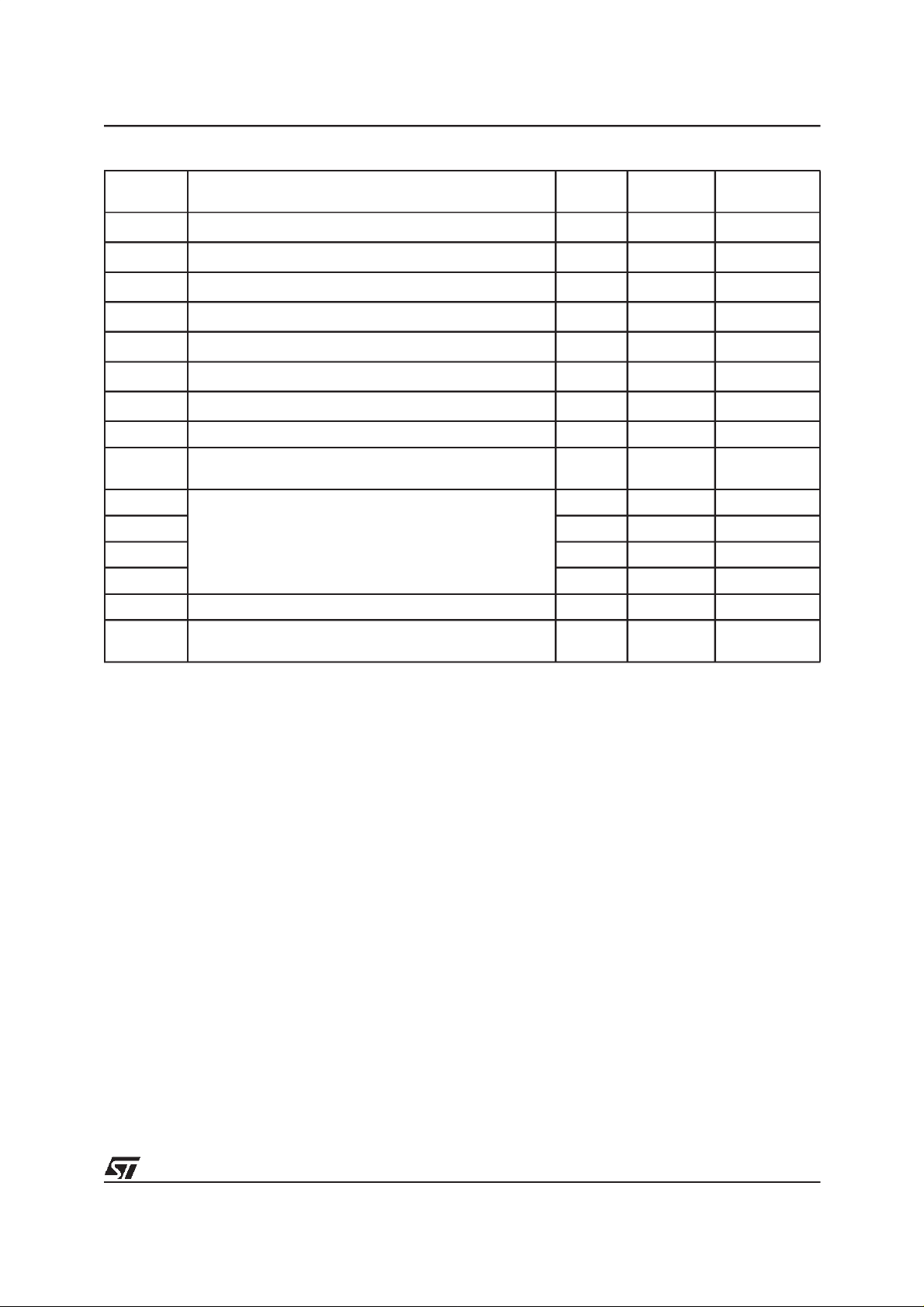
D10, D15, D20, D22, C20, C30
MICROMODULES
Memory Micromodules
General Information for D1, D2 and C Packaging
■ Micromodules were developed specifically for
embedding in Smartcards and Memory Cards
■ The Micromodule provides:
– Support for the chip
– Electrical contacts
– Suitable embedding interface for gluing the
module to the plastic package
■ Physical dimensionsand contact positions
compliant to the ISO 7816 standard
■ Micromodules delivered asa continuousSuper
35 mm tape. (This differsfrom the standard
35 mm tape in the spacing distance between
the indexing holes.)
DESCRIPTION
Memory Cards consist of two main parts: the
plastic card, and the embedded Micromodule
(which, in turn, carries the silicon chip).
The plastic card is made of PVC, ABS or similar
material, and can be over-printed with graphics,
text, and magnetic strips. The Micromodule is
embedded in a cavity in the plastic card.
The Micromodules are mounted on Super 35 mm
metallized epoxy tape, and are delivered on reels.
These contain all of the chips from a number of
wafers, including thosechips that were found to be
non-functioning during testing. Traceability is
ensured by a label fixed on the reel.
potting side contact side
D15
11
D10
D20
D22
C30 C20
1
11
1
1
1
Table 1. Memory Card and Memory Tag Integrated Circuits
Module
D10 ST1200, ST1305B, ST1331, ST1333, ST1335, ST1336, ST1353, ST1355
D15 ST14C02, ST1305B, ST1335, ST1336, ST1355
D20 ST14C02, M14C04, M14C16, M14C32
D22 M14C64, M14128, M14256
C30 M35101, M35102
C20 M35101, M35102
Please see the data briefing sheets of these products for example illustrations of these
micromodules
1/13December 1999
MICROMODULES
Table 2. Memory Card Products
Type
ST14C02C
M14C04
M14C16
M14C32
M14C64
M14128
M14256
ST1200 Memory Card IC, 256 bitOTP EPROM with Lock-Out 3.5 µm NMOS D10
ST1305B
Description (please see the individual product data
sheets for full specifications)
2
Memory Card IC, 2 Kbit (256 x 8) Serial I
2
Memory Card IC, 4 Kbit Serial I
Memory Card IC, 16 Kbit Serial I
Memory Card IC, 32 Kbit Serial I
Memory Card IC, 64 Kbit Serial I
Memory Card IC, 128 Kbit Serial I
Memory Card IC, 256 Kbit Serial I
Memory Card IC, 192 bitHigh Endurance EEPROM
with Secure Logic Access Control
C Bus EEPROM
2
C Bus EEPROM
2
C Bus EEPROM
2
C Bus EEPROM
2
2
C Bus EEPROM
C Bus EEPROM
C Bus EEPROM
Process Technology Module Style
1.2 µm CMOS D15, D20
0.6 µm CMOS D20
0.6 µm CMOS D20
0.6 µm CMOS D20
0.6 µm CMOS D22
0.6 µm CMOS D22
0.6 µm CMOS D22
1.5 µm CMOS D10, D15
ST1331
ST1333 1.2 µm CMOS D10
ST1335 1.2 µm CMOS D10, D15
ST1336 1.2 µm CMOS D10, D15
M35101 Contactless Memory Chip, 13.56 MHz, 2048 bit EEPROM 0.6 µm CMOS C20, C30
M35102
The assembly flows is as follows:
1. Dice sawing
2. Dice attach
3. Wire bonding
4. Potting
5. Milling (depending on product)
The range of products and types of Micromodule
are summarizedin Table 1 and Table 2. For large
volumes, ST is able to offer customized module
tape.
DELIVERY
The Super 35mm metallized epoxy tape is
delivered on reels, as shown in Figure 1. These
contain all of the chips from a number of wafers,
including those chips that were found to be nonfunctioning during testing. Traceability is ensured
by alabel fixed on the reel.
The typical quantity is 10,000 modules per reel,
with priority given to lot integrity on the reel. The
maximum quantity is 15,000 per reel.
Parts which are faulty (mechanically or electrically
defective) are identified by punch holes. The
specification for the reject punch holes is shown in
Memory Card IC, 272 bitHigh Endurance EEPROM
with Advanced Security Mechanisms
Contactless Memory Chip with 64-bit Unique ID,
13.56 MHz, 2048 bit EEPROM
Figure 4 for the D10 micromodule, in Figure 5 for
the D15 micromodule, in Figure 6 for the D20
micromodule, and in Figure 7 for the D22
micromodule.
Tape joins (tape splicing) are never more than 10
per 10 metre length, as shown in Figure 2 and
Figure 3.
At least 2.1 m of leader, and 2.1 m of trailer is
included oneach reel. Eachis made ofPVC Super
35 mm tape, without metalisation, and is opaque
to infrared and white light.
A “failure”marking of reject holes is included at the
beginning and end of the tape of a minimum of 5
consecutive module pitches (double positions).
Modules should be stored within the temperature
range -40 °Cto+85°C, for no more than 1 year.
Each reel ispacked in an antistatic bag, alongwith
a desiccant bag, and a humidity indicator card.
This cardindicates the level ofhumidity as follows:
30 - Blue: protection assured
40 - Pink: renew the desiccant bag
50 - Pink: protection no longer ensured
Three selfadhesive plastic identification labelsare
attached: one to the reel, one to the antistatic bag,
1.2 µm CMOS D10
0.6 µm CMOS C20, C30
2/13
MICROMODULES
Table 3. Manufacturing Flow and Manufacturing Facility Locations
Operation Location and Facility
Wafer Diffusion
Electrical WaferTest
Assembly Casablanca, Morocco.
Final Test
Table 4. Material Specification
Material Description
Basic material MCTS T2 or IBIDEN rough, typical thickness 120 µm
Adhesive Modified epoxy, typical thickness 18 µm
Laminated copper foil Typical thickness 35 µm
Adhesive strength
Tape Surface
Surface roughness Typically Rz: 3-12 µm at first accepted delivery
Contact surface Nickel-gold, galvanised treatment
Nickel thickness 2 µm (min.)
Gold thickness contact side, 0.1 µm (min.)
Totaltape thickness 160 ± 30 µm
Rousset, France.6” wafer fab.
Agrate, Italy.6” wafer fab.: standard EEPROM only
Rousset, France.
Agrate, Italy: standard EEPROM only
Rousset, France.
Casablanca, Morocco.
Tape
> 0.8 N/mm at room temperature. Monitored by the tape manufacturer using
appropriate test methods
The whole epoxy adhesive surface is controlled to be free of dirt, grease,cleaning
compounds and parting compounds
Control, Palmer “Special flat” diameter 3 mm, F = 1.5 N
Chip Interconnect
Dice bonding Silver epoxy
Bonding wire Gold 25 µm
Ring (D22 only) Bronze
Protective coating
Material UV epoxy,Black epoxy
Assembly Casablanca, Morocco.
3/13
MICROMODULES
and one to the reel box. Each label carries the
following information:
– PRODUCT: sales type
– LOT NUMBER: reel number
– POS: total number of positions
– GOOD: number of good positions
– FAIL: number of fail positions
– DATE: date of sealing
In addition, the antistatic bag and the delivery box
carry a self adhesive plastic “ESD” warning label,
85 x38 mm in size, indicating “Electrostatic
sensitive devices”.
Each reelis packed ina reel box,made ofrecycled
cardboard. The size of the reel boxdepends on its
origin. Several reel boxes arepacked in a delivery
box, which is also made of recycled cardboard.
A delivery note is provided, listing the following
information:
– Date of sealing
– Reel numbers
– Total number of positions, with the details of
positions per reel
– Order number and customer name
– Sales type
– Tape type
RECOMMENDED ACCEPTANCECRITERIA
The product identity should be checked against
the delivery documentation, and the quantity of
good positions on the reel recorded. The product
may be tested in accordance with the appropriate
data sheet, the conditions depending on the
product type, and the ISSUERor USER mode (for
ST13xx products).
For delivery acceptance, ST recommends
sampling the Micromodules from the beginning of
the reel. The sampling AQL should be applied, to
the ISO 2859 standard (test level II, normal test).
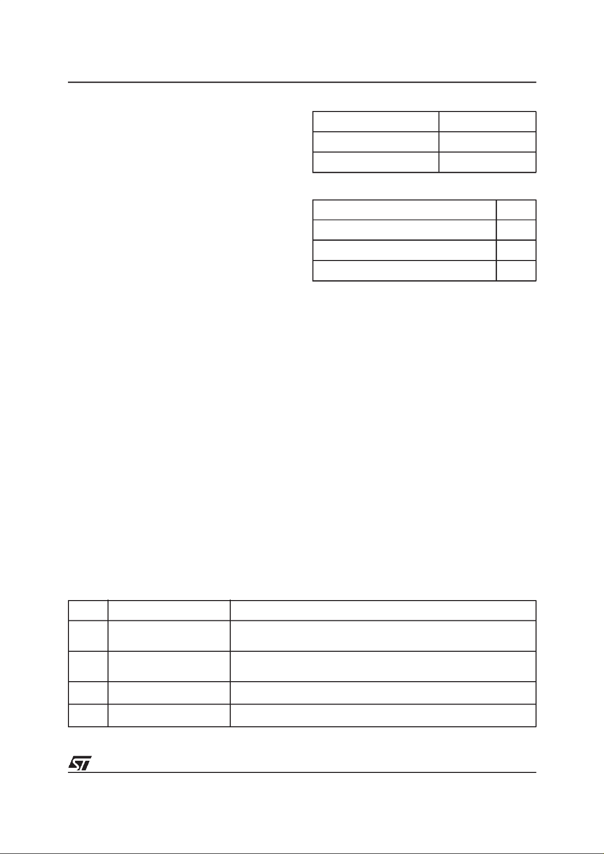
Table 5. Size of the Reel Box
Manufacturing Location Size of Reel Box
Rousset 370 x 390 x 80 mm
Casablanca 373 x 370 x 78 mm
Table 6. AQL Levels
Defect AQL
Totaldefects - mechanical and electrical 0.65
Mechanical defects 0.65
Electrical defects 0.65
Any observed discrepancies should bereported in
writing to the ST quality department. Table 6
shows the recommendedAQL levels.
The visual and mechanical test specification and
test conditions are described in Table 7.
Defect Acceptance Rate
Each reel contains the stated number of defective
devices, distributed so that no more than 20% of
them are found in a contiguous block on the tape.
ST’s own quality acceptance standard guarantees
that the customer will be informed when the
electrical yield is less than 90%.
The part numbers and re-ordering information will
be set according to ST’s current product coding
policy, as shown on the individual product data
sheets, or asagreed with the customer.
Reels that do not pass inspection should be
returned to ST within 15 working days after
delivery.
Table 7. Visual and Mechanical Specification and Test Conditions
Test Description and Method Reject Criteria
1 Contact area
2 Chip covering
1
3
1
4
Note: 1. Test 3 and 4 are conducted in accordance with MIL-STD-833.
Die bond strength Die shear force < 10 N
Wire bonding Wire lift or broken at pull test with < 4 g
Glue or particles, scratches print, severdefects on contact area
damaging the gold layer. Visual test distance 30 cm, naked eye.
Thickness and external dimension measurement exceeding total
thickness, or other dimensions not complying to the drawings
4/13

MICROMODULES
RELIABILITY
Product qualification and on-going reliability
monitoring is performed by ST. The principal steps
are listed in Table 8 and Table 9.
Table 8. Package Related Tests
Test Description Method Condition LPTD
1 Geometry ST Specification Monitoring/Lot 5 0/45
2 Visual inspection ST Specification Outgoing/Lot AQL= 0.040 0/315
3 Temperature cycling
Salt atmosphere
4
corrosion of contacts
5 Moisture resistance
Vibration with electrical
6
measurement
7 Bending properties ISO/IEC 7816-1
8 Torsionproperties ISO/IEC 7816-1
Note: 1. The notation
sample of 45devices taken from a lot, with the whole lot only accepted if every one of the 45 sample devices passed the test.
m/n
means: reject the whole lot if more thanmdevices fail from a sample ofndevices. For instance, 0/45 means a
MIL-STD-883
Method 1010
MIL-STD-883
Method 1009
MIL-STD-883
Method 1004
ISO/IEC 10373
-40 °Cto150°C,100 cycles 5 0/45
35 °C, 5% NaCl, 24 hour 15 0/15
85 °C, 85% HR Biased 5.5 V,
168 hour
1 octave/minute, acceleration up to
10 G (repeated 20 times)
measurement memory check at 25 °C
Long side: deflection 2 cm
Short side: deflection 1 cm
30 bendings per minute
Maximum displacement 15°±1°
1000 torsions, 30 torsions per minute
applied on long side only
7 0/32
20 0/11
20 0/11
20 0/11
Criteria
(note 1)
Table 9. Product Related Tests
Test Description Method Condition LPTD Criteria
1 Life test MIL-STD-883
Method 1005
2 Electrostatic discharge MIL-STD-883
Electrostatic discharge MIL-STD-883
3 Data retention,
Temperature storage
4 Write/Erase cycles ST Specification 100,000 Cycles 200 ppm/
5 Magnetic field, memory
check
6 X-rays, memory check ISO IEC 10373 70 kV,0.1 Grey 15 1/25
7 UV light,memory check ISO IEC 10373
Method 3015
Method 3015
MIL-STD-883
Method 1005
ISO IEC 10373 79,500 A/m 15 1/25
140 °C, 6 V,504 hours measurement
memory check at 25 °C
Human body model:
1.5 kΩ,100 pF,± 5000 V
Machine model: 0 Ω, 200 pF,± 200 V
measurement memory check at 25 °C
150 °C, 1000 hours, no bias
measurement memory check at 25 °C
2
15 W.s/cm
, 30 minutes maximum
3 0/76
n/a 0/9
n/a 0/9
5 0/45
0/32
1024 byte/
1000 cycle
15 1/25
5/13

Figure 1. Reel and Winding Direction
MICROMODULES
6/13

MICROMODULES
Figure 2. D10, D20, D22 Tape Join Specification
7/13

Figure 3. D15 Tape Join Specification
MICROMODULES
I
21
654 3
H
G
F
E
D
C
B
DATUM
06/1998
SCALE
A
DRAWN BY:
STEFFEN.F
CONTROLED BY:
ROYER.G
A
21
GRAPHICS REV.
JOIN
( Sproket holes axis straightness)
SUPER 35 6 CONTACTS MICROMODULE:
Z.I. de Rousset
Fax (33) 42.53.22.88
Tel. (33) 42.25.88.00
0.2/16
Copyright SGS-THOMSON Microelectronics. Unauthorized reproduction and communication is stricly proh
GRAPHIC TITLE:
B.P. 2 - 13106 ROUSSET CEDEX
654 3
12 11 10 9 8 7
I
H
G
F
E
7
area
98
* Measurements are subject to change without notice.
DIMENSIONS ARE IN MILIMETERS
10
11
NOTES:
-Total thickness in splice area is 0.300 Typical
-Reject hole and sproket holes are punched free in splice
-Assy reject holes (M) may be punched in splice area ( see (M) in POA for location )
-Joint is on contact side only
D
C
B
12
A
8/13

MICROMODULES
Figure 4. D10 Micromodule Outline
1
1
11
CONTACT SIDE
1
1
X
11
Y
9/13
CROSS SECTION
O
POTTING SIDE

Figure 5. D15 Micromodule Outline
DIE SIDE
CROSS SECTION
0.58 max
R1.3
max
7
10.8
7.62
0.16
0.1
NOTE:
- (P) is reject identification hole ø2.2
- (M) may be punched with (P): center positioning ±0.2
- Sproket holes may be with or without metalisation
- Recommended punching contour for the customer: 8.32*11 R1.4
- Minimal contact area according to ISO 7816-1
GENERAL TOLERANCE IS ±0.1 mm
ALL DIMENSIONS ARE IN MILLIMETERS
Measurements are subject
CONTACT SIDE
8.12
2.6min
2.2min
2.54
to change without notice
9.5
1.422
R0.15
1.422
(P)ø2.2
35
31.83
27±0.2
23.015
12.8±0.2
8.815
4.75
(M)ø1.5
Copyright SGS-THOMSON Microelectronics. Unauthorized reproduction and communication is stricly
GRAPHIC TITLE:
Z.I. de Rousset
B.P. 2 - 13106 ROUSSET CEDEX
Tel. (33) 42.25.88.00
Fax (33) 42.53.22.88
POA FOR MICROMODULE D15
3±0.2
5.2±0.2
PACKAGE CODE
FU
SCALE
none
GRAPHICS REV.
A
DATUM
06/1998
DRAWN BY:
ROYER.G
CONTROLED BY:
STEFFEN.F
MICROMODULES
10/13

MICROMODULES
Figure 6. D20 Micromodule Outline
1
1
11
CONTACT SIDE
1
1
X
11
Y
11/13
CROSS SECTION
O
POTTING SIDE

Figure 7. D22 Micromodule Outline
O
CONTACT SIDE
MICROMODULES
CROSS SECTION
POTTING SIDE
O
12/13

MICROMODULES
Information furnished is believed to be accurate and reliable. However, STMicroelectronics assumes no responsibility for the consequences
of useof such information norforany infringement of patents orotherrights of third parties which mayresult from itsuse. No license is granted
by implication or otherwise under any patent or patent rights of STMicroelectronics. Specifications mentioned in this publication are subject
to change without notice. This publication supersedes and replaces all information previously supplied. STMicroelectronics products arenot
authorized for use as critical components in life support devices or systems without express writtenapproval of STMicroelectronics.
1999 STMicroelectronics - All Rights Reserved
The ST logo is a registered trademark of STMicroelectronics.
All other names are the property of their respective owners.
STMicroelectronics GROUP OF COMPANIES
Australia - Brazil - China - Finland - France - Germany - Hong Kong -India - Italy - Japan -Malaysia - Malta - Morocco - Singapore - Spain -
Sweden - Switzerland - United Kingdom - U.S.A.
http://www.st.com
13/13
 Loading...