

CLP270M
ApplicationSpecific Discretes
A.S.D.
OVERVOLTAGE AND OVERCURRENT
PROTECTION FOR TELECOM LINE
MAINAPPLICATIONS
Any telecom equipment submitted to transient
overvoltagesandlightningstrikes suchas:
Analogand ISDNline cards
PABX
MainDistribution Frames
Primaryprotection modules
DESCRIPTION
The CLP270M is designed to protect
telecommunicationequipment. It provides both a
transient overvoltage protection and an
overcurrentprotection.
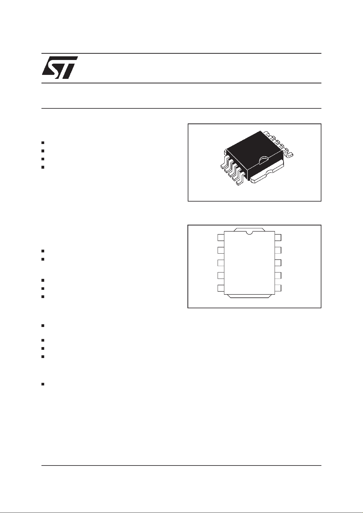
It is housedin a PowerSO-10
TM
package.
FEATURES
DUALBIDIRECTIONALPROTECTIONDEVICE.
HIGHPEAKPULSE CURRENT:
Ipp = 100A(10/1000µs SURGE)
Ipp = 500A(2/10µs SURGE)
MAX.VOLTAGEAT SWITCHING-ON: 380V
MIN.CURRENT AT SWITCHING-OFF : 150mA
FAILURESTATUSOUTPUTPIN
PowerSO-10
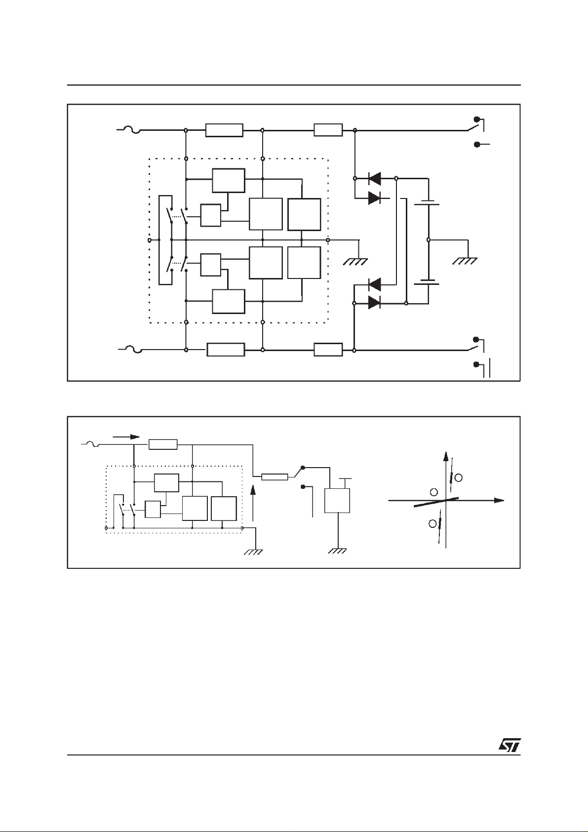
SCHEMATICDIAGRAM
1
TIP
S
TIP
L
TIP
L
TIP
L
TABis connected to GND
PRELIMINARY DATASHEET
TM
NCFS
RING
S
RING
L
RING
L
RING
L
BENEFITS
Both primary and secondaryprotectionlevelsin
onedevice.
Voltageand current controlledsuppression.
TM
SurfaceMountingwithPowerSO-10
package.
Line card cost reduction thanks to the very low
power rating of external components required :
balanced resistors, ring relay, low voltage SLIC
protection.
Falls into short circuit if destroyed,still ensuring
protection.
January1998 - Ed: 5B 1/24

CLP270M
COMPLIESWITHTHE
FOLLOWING STANDARDS:
Peak Surge
Voltage
(V)
Voltage
Waveform
(µs)
Current
Waveform
(µs)
Admissible
Ipp
(A)
Necessary
ITUK20 4000 10/700 5/310 100 VDE0433 4000 10/700 5/310 100 VDE0878 4000 1.2/50 1/20 100 IEC-1000-4-5 level4
level4
FCCPart68,lightning surge
type A
FCCPart68,lightning surge
1500
800
100 9/720 5/320 25 -
10/700
1.2/50
10/160
10/560
5/310
8/20
10/160
10/560
100
100
200
100
type B
BELLCORETR-NWT-001089
Firstlevel
BELLCORETR-NWT-001089
2500
1000
2/10
10/1000
2/10
10/1000
500
100
5000 2/10 2/10 500 -
Secondlevel
CNETl31-24 4000 0.5/700 0.8/310 100 -
BLOCKDIAGRAM
Resistor
(Ω)
-
-
-
-
-
-
270
270
Pin Symbol Description
1 FS FailureStatus
2 TIPS TIP (SLICside)
3 / 4/ 5 TIPL TIP (Lineside)
6 / 7/ 8 RINGL
9 RINGS
RING(Lineside)
RING(SLICside)
10 NC Not connected
TAB GND Ground
2/24

CLP270M
APPLICATION NOTE
1.INTRODUCTION
This deviceincludesa primaryprotection level and is suitablefor main distribution frames and line cards.
This protection concept is explained and, in addition, the CLP270M performances are analysed when
facingdifferentsurgesasdescribedin the BELLCOREGR 1089 recommendations.
Fig. 1:
Subscriberline protectiontopology
Telecommunication
line
Telecommunication
line
“PRIMARYPROTECTION”
CLP270M
MDF
EXCHANGE
CLP270M
MDF
EXCHANGE
“SECONDARYPROTECTION”
SLIC
LINE CARD
“SECONDARYPROTECTION”
THDTxx
or
LCP1511D
or
LCDP1511D
LINE CARD
SLIC
Figure1is a simplifiedblock diagramof a subscriberline protectionthatiscommonlyused.
Thisshows two differenttopologies:
A ”primaryprotection”locatedon the Main DistributionFrame(MDF)eliminates coarselythe highenergy
environmentaldisturbances(lightningtransientsand AC power mainsdisturbances)
A ”secondary protection” located on the line card includes a primaryprotectionlevel (first stage) and a
residualprotection(secondstage)which eliminatesfinelytheremainingtransientsthathavenotbeentotally
suppressedbythefirststage.
2. STMicroelectronicsCLP270MCONCEPT
2.1.Evolutionof the SLICprotection
Over the years, t he silicon protect ion pe rformances ha v e co nsiderab ly cha nge d.
The first generation of products like SMTHBTxx and SMTHDTxx offered fixed overvoltage protection
againstsurges on eitherTIPor RINGlinein fourpackages.
The following generation like THBTxx and
THDTxx still offered fixed overvoltage protection
againstsurges on both TIP and RING lines in two
packages.
The next step was the introduction of the
LCP1511D which brought the advantage of full
programmablevoltage.
Today, the CLP270Mcombinesthe features of all
thepreviousgenerations.In additiontothat,itoffers
Fig. 2:
Linecard protection
Programmable
thanks to any
external voltage
reference
+I
SWON
I
Programmable
thanks to an
externalresistor
V
an overcurrentdetection when operatingin speech
modeandalso aFailureStatus output signal.
The figure 2 summarizes the firing modes of the
CLP270M which basically hold the SLIC inside its
correctvoltageand currentvalues.
-I
SWON
Line card
operating
conditions
3/24

CLP270M
2.2Application circuit:CLP270M in line card.
Fig.3 :
TIP
RING
CLP270Min linecard
Fuse
Rsense
TIPL TIPS
Overcurrent
detector
Ov v
RINGS
er oltage
ref
erence
(+/- 270V)
Overvoltage
reference
(+/- 270 V)
Overvoltage
OR
SW3 SW1
FS GND
Fuse
SW4 SW2
RINGL
OR
Overcurrent
Rsense
detector
detector
Overvoltage
detector
I
-Vbat
TIP
-Vbat
(*)
SLIC
RING
Rp
Rp
1
2
1
2
External
voltage
reference
Ring
Generator
(*) LCP1511D orTHDT seriesor LCDP1511D
Figure 3 above shows the topology of a protected analog subscriber line at the exchange side. The
CLP270Misconnectedto theringrelay viatwo balancedRp resistors,and totheSubscriberLine Interface
Circuit. A second device is located near the SLIC : it can be either a LCP1511D, a THDT series or a
LCDP1511D.
Thesetwo devicesare complementaryand their functionsare explainedbelow :
The first stage based on CLP270Mmanages the high powerissued from the external surges. When
used in ringing mode, the CLP270M operates in voltage mode and provides a symmetrical and
bidirectional overvoltage protection at +/- 270 V on both TIP and RING lines. When used in speech
mode, the CLP270Moperates in current modeandthe activationcurrent of the CLP270M is adjusted
sense
.
by R
The second stage is the external voltage reference device which defines the firing threshold voltage
during the speech mode and also assumes a residualpowerovervoltagesuppression. This protection
stage can be either a fixed or programmable breakover device. The THDTxx family acts as a fixed
breakoverdevice whiletheLCP1511Dor the LCDP1511Doperatesas a programmableprotection.
Thankstothistopology, thesurgecurrentinthelineisreducedafterthe CLP270M.Becausetheremaining
surge energy is low, the power ratings of Rp, the ring relay contactsand the external voltage reference
circuitcan bedownsized.Thisresultsin asignificantcost reduction.
4/24

CLP270M
Fig.4:
Switchingby voltageduringringingmode.
ILG
Fuse
TIP
FS
Rsense
TIPL TIPS
Overcurrent
detector
OR
SW3 SW1
Overvoltage
detector
1/2 CLP270M
Overvoltage
reference
(+/- 270V)
GND
ILG
1
Rp
VLG
2
-270
3
A1
2
1
V
+270
2.3.Ringingmode
Inringingmode(Ring relay in position2),the onlyprotectiondeviceinvolvedis theCLP270M.
Innormalconditions, theCLP270M operatesin region1ofA1curve,and is idle.
If an overvoltage occuring between TIP(or RING)andGND reaches the internalovervoltagereference
(+/- 270 V), the CLP270M acts and the line is short-circuited to GND. At this time the operating point
moves to region 2 for positive surges(region 3 fornegativesurges). Once thesurge currentfalls below
the switch offcurrent I
, the devicereturns to its initial state (region 1).
SWOFF
For surges occuring between TIP and RING, the CLP270Macts in the same way. This means that the
CLP270Mensures a tripolarprotection.
Whenused alone, theCLP270Macts at the internalovervoltagereferencelevel (+/- 270 V). Furthermore,
it ispossibleto adjust this thresholdlevel toa lowervoltageby using:
up to 4 fixedexternal voltage reference(V
externalreferencesupplies,V
andVb2(seefig.5b,onnextpage).
b1
toVZ4) (see fig. 5a, here-below).
Z1
Fig.5a: Methodtoadjustthe referencevoltage.
1
2
1
2
TIP
RING
Fuse
Rsense
TIPL TIPS
Overcurrent
detector
detector
RINGS
Overvoltage
reference
(+/- 270 V)
Overvoltage
reference
(+/- 270 V)
detector
Overvoltage
Overvoltage
detector
OR
SW3 SW1
FS GND
SW4 SW2
OR
Overcurrent
RINGL
Rsense
Fuse
Rp
VZ1
VZ2
VZ3
VZ4
Rp
5/24
CLP270M
Fig. 5b:
Methodto adjustthe referencevoltage
TIP
Fuse
Rsense
.
1
Rp
TIPL TIPS
Overcurrent
detector
Overvoltage
detector
Overvoltage
detector
RINGS
RING
OR
SW3 SW1
FS GND
SW4 SW2
RINGL
OR
Overcurrent
detector
Rsense
Fuse
Fig. 6: Switchingby currentduring speechmode.
Fuse
TIP
ILG
Rsense
TIPL TIPS
Overcurrent
detector
Overvoltage
Overvoltage
detector
OR
SW3 SW1
FS
reference
(+/- 270 V)
Rp
VLG
GND
Overvoltage
reference
(+/- 270 V)
Overvoltage
reference
(+/- 270 V)
1
2
Rp
External
voltage
reference
-Vbat
-VREF2
2
VB1
VB2
1
2
ILG
A2
5
4
VREF1
6
V
LG
2.4. Speechmode
Inspeechmode (Ring relay in position 1), the protectionis providedbythe combinationof bothCLP270M
andthe externalvoltagereferencedevice.
Innormalconditions,theworkingpointof thiscircuitis locatedinregion4 ofA2 curve: theCLP270Mis idle.
Whena surgeoccursonthe line,theexternalvoltagereferencedeviceclampsatGND or-V
respectively
bat
forpositiveand negativesurges.
This generates a current which is detected by R
and causes the protection to act : the line is
sense
short-circuitedto GND.
Theoperating point movesto region5 forpositivesurges or region6 for negativesurges.
Oncethe surge currentfalls below the switching-offcurrentI
, the CLP270Mreturnsto its initial state
SWOFF
(region4).
6/24

CLP270M
Fig.7a and7b: Switching-oncurrentversus R
sense
.
ISWON(T,Rsense) / ISWON(25°C,4 )Ω
2
@-20°C @25°C @75°C
1
Iswon @ 25°C (mA)
500
300
Iswonmin
negative
Iswonmax
negative
Iswonmin
positive
Iswonmax
positive
200
0.5
100
0.3
50
0.2
3 5 7 9 11 13
357911
Rsense ( )Ω
Rsense ( )Ω
Thechoice of the switching-oncurrents is functionof theR
sense
resistors.
In normal operating condition the current (typically below -100 mA) should not activate the protection
deviceCLP270M.Thereforethe level ofactivationis tobechosenjustabovethislimit(-200mA).Thislevel
isadjustedthrough R
Figures7a and 7b enable the designerstochoosethe right R
sense
.
value.
sense
EXAMPLE :
ThechoiceofR
=4Ωensuresa negativetriggeringof-190mA minand-320 mAmax.Inthiscase,the
sense
positivetriggeringwillbe 150mAminand280 mA max.
2.5.FailureStatus
TheCLP270Mhasan internalfeaturethat allowsthe usertoget a FailureStatus (FS)indication.Whenthe
CLP270Mis short-circuitingthe line to GND, a signal can be managed through pin 1. This signal can be
used to turn a LED on in order to provide a surge indication.It may also be used with a logic circuitry to
countthenumberof disturbancesappearingon thelines.
If a surge exceeding the maximum ratings of the CLP270M occurs on the line, the device will fail in a
short-circuit state.
Fig.8: FailureStatus circuitand diagnostic.
Fig.9: Operationlimitsanddestructionzoneof the
CLP270M.
FAILURE
STATUS
Rsense
1
CLP270M
1k
Rsense
+12V
5 000
2 000
1 000
500
200
100
50
20
10
0.01 0.02 0.05 0.1 0.2 0.5 1 2 5 10
t (ms)
Thefigure9 showstwo differentcurves:
The loweroneindicates the maximumguarantedworkinglimitsoftheCLP270M.
The upper curve shows the limit above which the CLP270M is completelydestructed. In thiscase, the
FailDiagnosticpin is on.
7/24

CLP270M
3. CLP270MTESTRESULTSACCORDING TO BELLCORE 1089 REQUIREMENTS.
3.1. BELLCOREGR-1089-CORE requirements:
Table 1: Firstlevel lightningsurge.
Surge Minimum
1 +/-600 100 10/1000 25 A
2 +/-1000 100 10/360 25 A
3 +/-1000 100 10/1000 25 A
4 +/-2500 500 2/10 10 B
5 +/-1000 25 10/360 5 B
Table2:
Secondlevel lightningsurge.
Surge Minimum
peak voltage
(volts)
peakvoltage
(volts)
Minimum
peakcurrent
per conductor
(Amps)
Minimum
peak current
per conductor
(Amps)
Maximumrise
/ Minimum
decay time for
voltageand
current
(µs)
Maximumrise
/ Minimum
decaytimefor
voltageand
current
(µs)
Repetitions,
eachpolarity
Repetitions,
eachpolarity
Test
connections
per
table4.1
Test
connections
per
table4.1
1 +/- 5000 500 2/10 1 B
Tables1 and2 summarizethe lighting surgesrequired by the bellcore 1089.
8/24

Table3: First level ACpower fault (table 4-7 of GR-1089-COREissue 2, december1997).
CLP270M
Test Voltage
(V
RMS
)
Shortcircuit
currentper
Duration Primary
protection
connections
conductor
(Amps)
table4.1
1 50 0.33 15 minutes Removed A
2 100 0.17 15 minutes Removed A
3 200,400
and 600
1 (at 600V) 601s
applicationof
Removed A
each voltage
4 1000 1 60 1s
applications
Operative
protectorin
place
5 see figure 4-3 see figure 4-3 60 5s
Removed seefigure4-3
applications
6 600 0.5 30s Removed A
7 600 2.2 2s Removed A
8 600 3 1s Removed A
9 1000 5 0.5s Operative
protectorin
place
Test
per
B
B
Table4:
Secondlevel AC power fault (table4-8 of GR-1089-COREissue 2, december1997).
Test Test for Voltage
1 Secondary
contact
2 Primary
contact
3 Short-term
fault induction
4 Long-term
fault induction
5 Highimpedance
induction
Test
connections
per
table4.1
(V
RMS
Shortcircuit
)
currentper
Duration
conductor
(Amps)
120,277 25 15minutes A
600 60 5 seconds A
600 7 5 seconds A
100-600 2.2
15minutes A
(at600V)
15minutes
9/24

CLP270M
Table5:
Test connection(table4-1 of GR-1089-CORE).
Test Two-wireinterface Four-wire interface
A 1. Tipto generator,Ring to ground
1. Eachlead(T, R, T1, R1)to generatorwith
other threeleads grounded
2. Ringto generator,Tipto ground
2. Tipand Ringto generatorsimultaneously,
T1 andR1 to ground
3. Tipto generator,Ring to generator
simultaneously
B Tip to generator,Ring to generator
3. T1and R1 to generatorsimultaneously,
Tip and Ring to ground
T, R, T1, R1 to generatorsimultaneously
simultaneously
S1
Switch
unit
under
test
Voltage
Source
Limiting
resistance
(IF specified)
S2
S3
S4
T
E
R
M
T
E
R
M
Test
Table6:
Applicationof lightning and AC power faulttest voltages (table 4-2 of GR-1089-CORE).
Test S1 S2 S3 S4
T to generator,Rto ground
Closed Open Open Closed
(conditionA1 of table4-1)
R to generator,T toground
Open Closed Closed Open
(conditionA2 of table4-1)
T to generator,Rto generator
Closed Open Closed Open
simultaneously
(conditionA3 of table4-1)
Tables1 to 6 summarizethesurgeneedsdefinedbyBellcoreregarding both lightningand ACpowerfault.
Incase of first leveltest, the equipmentundertestshallbe operatingafter thesurge. For the second level
tests,the equipment undertest maybedamaged,but no fire or electricalsafety hazard mayoccur.
10/24

CLP270M
3.2.Firstlevel lightningsurge:
3.2.1.ringingmode
Lightningphenomenaarethe mostcommonsurgecauses.Thepurposeof thistestis tocheckthe behavior
oftheCLP270Magainsttheselightning strikes.
Fig.10:
Lightningsimulationtest.
2/10 µs
GENERATOR
I1
4
Rsense
TIPL TIPS
Rp
+/- 2.5 kV
(500 A)
1/2 CLP270M
GND
V1
Figures11and 12showthatthe remainingovervoltagedoesnotexceed+/- 500V. TheCLP270Mswitches
onwithin250ns and withstandsthe500Agiven by the BELLCORE2/10µs generator.
Fig.11:
CLP270Mresponseto a positivesurge.
Fig.12 :
CLP270Mresponsetoa negativesurge.
3.2.2.Speechmode
Fig.13:
Lightningtest in speech mode.
2/10 µs
GENERATOR
+/- 5 kV
(500 A)
I
1
TIPL
1/2 CLP270M
4
Rsense
TIPS
GND
50
Rp
V1
I2
-48V
LCP1511D
SLIC
V2
11/24

CLP270M
Fig.14: CLP270Mresponsetoa positivesurge. Fig.15:CLP270Mreponsetoa negativesurge.
Figures14 and15 givethe voltageandcurrentbehaviorduring positiveandnegative2.5kV,2/10µs,500A
surge tests using a LCP1511D as second stage protection device. The firing threshold values are now
adjustedto GNDand to -Vbat(-48V) by theactionof thesecond stageprotectionwhichactsasan external
voltagereference.
Asshown onthesefigures,the maximumremainingvoltagedoesnot exceed+8.5Vfor positivesurgesand
-65Vfor negative surges.
12/24

3.3.Secondlevel lightningsurge
3.3.1.Lightningtest in ringing mode
Fig.16: Lightningtest in Ringing mode.
CLP270M
2/10 µs
GENERATOR
+/- 5 kV
(500 A)
Fig.17:
CLP270Mresponseto a positivesurge.
IV11
Rsense
TIPL
1/2 CLP270M
GND
4
Rp
TIPS
Fig.18:CLP270Mresponseto a negativesurge.
Thefigures17and18givethevoltageandcurrent behaviorduringpositiveand negative5kV,2/10µs,500A
surgewith the CLP270Macting in Ringingmode.
13/24

CLP270M
3.3.2.Speechmode
Fig.19:
Fig.20:
Lightningtestin Speech mode.
2/10 µs
GENERATOR
+/- 5 kV
(500 A)
CLP270Mresponseto a positivesurge.
I
1
TIPL
1/2 CLP270M
4
Rsense
TIPS
GND
50
Rp
V1
I2
-48V
LCP1511D
SLIC
V2
Fig.21:CLP270Mresponseto a negativesurge.
Thefigures20and22givethevoltageandcurrent behaviorduringpositiveand negative5kV,2/10µs,500A
surgewith the CLP270Macting in speechmode.
TheCLP270M withstandsthe second level lightningsurgetest without trouble.
14/24

3.4.FIRSTAND SECOND LEVELACPOWERFAULT
3.4.1.Ringingmode
CLP270M
Fig.22:
AC powerfaulttestin Ringingmode.
I1
Rs
V(RMS)
50Hz
4
Rsense
TIPL TIPS
1/2 CLP270M
GND
Rp
V1
Fig.24: ACpowerfaulttest in Speech mode.
Fig. 23:
Example of behavior when facing test 3
(400V,600Ω).
Fig. 25:
Example of behavior when facing test 3
(400V,600Ω).
V(RMS)
50 Hz
I1
Rs
4Ω
Rsense
TIPL TIPS
1/2 CLP270M
GND
50
Ω
Rp
-48V
LCP1511D
SLIC
V2
Thefigures 23and 25 givethe voltageand currentatthe CLP270Mterminalsin Ringingmodeand Speech
mode.The CLP270Mis able to withstandallthefirstlevel AC power fault testsas requiredin thetable 4-7
ofGR-1089-COREstandard.
Forthe secondlevel AC power faulttestsserialprotectionas PTCor fuseareneeded.
Allthesecurves, lightningand AC powerfaultrepresentthe behaviorof theCLP270Min worst case tests,
anyhow the CLP270Mwithstandsall the otherssurges of the BellcoreGR1098 standard. For the second
levelACpowerfault test, the use of seriesprotectionelements(PTC or fuses)are needed.
15/24

CLP270M
ABSOLUTEMAXIMUMRATINGS (R
Symbol Parameter TestConditions Value Unit
SENSE
=4Ω, and T
amb
=25°C)
I
PP
Line to GNDpeak surge
current
10/1000µs (opencircuit voltage
wave shape10/1000µs)
5/310µs(opencircuit voltage
wave shape10/700µs)
2/10µs (opencircuit voltage
wave shape)
I
TSM
Non repetitivesurge peak
tp = 20 ms 60 A
on-statecurrent(TIPor
RINGversusGround)
F = 50 Hz
T
stg
T
j
T
L
Storagetemperature range
Maximumjunctiontemperature
Maximumleadtemperatureforsolderingduring10 s 260 °C
ELECTRICAL CHARACTERISTICS(R
SENSE
tp = 200 ms 30 A
tp = 2 s 15 A
=4Ω, andT
amb
Symbol Parameter Test Conditions
I
LGL
Line to GNDleakage
current
. VLG=240V
. MeasuredbetweenTIP
(or RING)and GND
V
ref
Overvoltageinternal
reference
. ILG=1mA
.MeasuredbetweenTIP
(or RING)and GND
V
SWON
I
SWOFF
Line to GNDvoltageat
SW1or SW2switching-on
Line to GNDcurrentat
. Measuredat50 Hzbetween
TIPL(orRINGL)and GND
. Refer to testcircuit page 17
SW1or SW2switching-off
(negativecurrent)
I
SWON
Line currentat SW1 or
SW2switching-on
C RINGto GNDcapacitance
TIP to GND capacitance
TIP to RINGcapacitance
. Positivepulse
Negativepulse
.
. V
V
.
.V
RINGL
TIPL
GND
=-1V
=-48V
=0V
.F = 1 MHz V
RMS
=25°C)
=1V
100 A
130
500
- 40 to + 150
°C
150
Value
Min. Typ. Max.
Unit
10 µA
270 V
380 V
150 mA
150
190
180
280
320
mA
pF
62
57
16/24

CLP270M
TEST CIRCUITFORI
SWOFF
PARAMETER: GO-NOGO TEST
R
D.U.T.
V
BAT
This is a GO-NOGOtest whichallows to confirmthe switch-off(I
TESTPROCEDURE:
- Adjust the currentlevel at the I
- Firethe D.U.T.witha surgecurrent : I
- The D.U.T.will comebacktotheOFF-statewithin a durationof 50msmax.
Fig. 26: Typi calrelativ evariationofswi t chi ng-oncurrent(positiv eor negati v e)versusR
junctiontemperature(seetestconditionFig.28).
ISWON (T, Rsense) / ISWON (25°C,4 )Ω
2
1
=
-48V
@-20°C @25°C @75°C
SWOFF
SENSE
SWOFF
valueby shortcircuitingthe D.U.T.
=10A, 10/1000µs.
PP
Fig. 27: Variation of switching-on current versus
resistorand
R
500
300
200
at 25°C.
SENSE
Iswon@ 25°C (mA)
) levelina functionaltest circuit.
Iswonmin
negative
Surge
generator
Iswonmax
Iswonmin
negative
positive
-V
P
Iswonmax
positive
0.5
0.3
0.2
3 5 7 9 11 13
Rsense ( )Ω
Fig. 28:I
MEASUREMENT
SWON
- Iswon = I1 when the CLP270M switches on (I1 is
progressivelyincreasedusing R)
- Both TIP and RING sides of the CLP270M are
checked
=10
48 V
.
Ω
RL
R sense
TIPL TIPS
DUT
RINGL RINGS
I1
GND
-R
L
±
100
50
357911
Rsense ( )Ω
Fig. 29: Relative variationof switching-offcurrent
versusjunctiontemperatureforR
SENSE
and 10Ω.
ISWOFF [Tj°C] / ISWOFF [25°C]
2.0
1.8
1.6
1.4
1.2
1.0
R
0.8
0.6
0.4
-40 -20 0 20 40 60 80
Tj(°C)
between3
17/24

CLP270M
Fig. 30:
versusR
Relativevariation of switching-off current
(between3 and10Ω).
SENSE
ISWOFF[Rsense] / ISWOFF[4 Ω]
1.6
1.4
1.2
1.0
0.8
0.6
0.4
46810
Rsense ( )Ω
Fig.31:
Residualcurrentl1 after theCLP270M.
The residualcurrent l1 is definedbyits peakvalue
(I
) and its duration (τ)@IP/2 (see below circuit
P
test).
Currentsurge input
waveform(µs)
I
(A)
PP
5/310
130A
SURGE
GENERATOR
positivesurge
negativesurge
TIPL TIPS
DUT
RINGLRING
R sense
Residualcurrent
afterthe CLP270M
Peak
waveform
current
(A)
I
P
4.2
1.1
R = 50 Ohms
I1
GND
S
t(µs)
1
0.5
-48V
Fig. 32: Relative variation of switching-onvoltage
versusdV/dt with an externalresistor of 4 Ω.
VSWON / REFV
1.12
1.10
1.08
1.06
1.04
1.02
1.00
0.98
0.1 0.3 1 3 10 30 100 300 1000
dV/dt (V/µs)
Fig. 33: Relative variation of internal reference
voltageversusjunctiontemperature(I
REF [Tj°C] /V [25°C]REF
V
1.10
1.05
1.00
0.95
0.90
0.85
-40 -20 0 20 40 60
Tj (°C)
=1mA).
LG
18/24

CLP270M
Fig. 34:
Typical junction capacitance (TIPL/GND)
versusapplied voltage.
C (pF)
220
200
180
160
140
120
100
80
60
40
0 102030405060
(V)
V
R
Fig. 35: Maximum non repetitive surge RMS on
statecurrentversusoverloadduration .
ITSM(A)
100
90
80
70
60
50
40
30
20
10
0
0.01 0.1 1 10 100 1000
TIP or RING
vs GND
t(s)
F=50Hz
Tj initial=25°C
19/24

CLP270M
SOLDERINGRECOMMENDATION
The soldering process causes considerable
thermal stress to a semiconductor component.
This has to be minimized to assure a reliable and
extended lifetime of the device. The
PowerSO-10
TM
package can be exposed to a
maximum temperature of 260°C for 10 seconds.
However a proper soldering of the package could
be done at 215°C for 3 seconds. Any solder
temperature profile should be within these limits.
As reflow techniques are most commonin surface
mounting, typical heating profiles are given in
Figure 36, either for mounting on FR4 or on
metal-backed boards. For each particular board,
the appropriate heat profile has to be adjusted
experimentally. The present proposal is just a
starting point. In any case, the following
precautionshaveto be considered:
- alwayspreheat the device
- peaktemperatureshouldbeat least30 °C
higherthan the meltingpointof the solder
alloychosen
- thermalcapacityof the basesubstrate
Fig36 :
Typical reflowsoldering heat profile
Temperature ( C)
250
o
o
245 C
Voids pose a difficult reliability problem for large
surface mount devices. Such voids under the
packageresultin poorthermalcontactandthehigh
thermal resistance leads to component failures.
The PowerSO-10 is designed from scratch to be
solely a surfacemount package,hencesymmetry
in the x- and y-axis gives the package excellent
weightbalance.Moreover, the PowerSO-10offers
the unique possibility to control easily the flatness
and quality of the soldering process. Both the top
and the bottomsolderededges of the packageare
accessible for visual inspection (soldering
meniscus).
Coplanarity between the substrate and the
package can be easily verified. The quality of the
solder joints is very important for two reasons : (I)
poor quality solder joints result directly in poor
reliability and (II) solder thickness affects the
thermal resistance significantly. Thus a tight
control of this parameter results in thermally
efficientand reliablesolder joints.
o
215 C
200
Soldering
Cooli ng
150
Epoxy FR4
board
Preheating
100
Metal-backed
50
board
0
0 40 80 120 160 200 2 40 280 320 360
Time (s )
20/24

CLP270M
SUBSTRATES ANDMOUNTINGINFORMATION
The use of epoxy FR4 boardsis quite commonfor
surface mounting techniques, however, their poor
thermal conduction compromises the otherwise
outstanding thermal performance of the
PowerSO-10. Some methods to overcome this
limitationarediscussedbelow.
One possibility to improvethe thermal conduction
is the use of large heat spreader areas at the
copper layer of the PC board. This leads to a
reductionof thermalresistanceto 35 °Cfor 6 cm
of theboardheatsink(see fig. 37).
Use ofcopper-filledthroughholesonconventional
decrease thermal resistance accordingly. Using
a configurationwith 16holesunderthe spreaderof
thepackage with a pitchof1.8mmanda diameter
of 0.7 mm, the thermal resistance (junction heatsink) can be reduced to 12°C/W(see fig. 38).
Besidethe thermaladvantage,thissolutionallows
multi-layer boards to be used. However, a
drawbackof thistraditionalmaterialpreventits use
in very high power, high current circuits. For
instance, it is not advisable to surface mount
devices with currents greater than 10 A on FR4
2
boards. A Power Mosfet or Schottky diode in a
surfacemount powerpackagecan handleup to
around50Aifbettersubstratesareused.
FR4 techniqueswill increase the metallizationand
Fig37 : Mountingon epoxyFR4 headdissipation by extendingthearea of the copperlayer
Copper foil
FR4 board
Fig38 : Mountingon epoxyFR4 byusingcopper-filled throughholes for heat transfer
Copperfoil
heattransferheatsink
FR4board
21/24

CLP270M
A new technology available today is IMS - an
Insulated Metallic Substrate. This offers greatly
enhanced thermal characteristics for surface
mount components.IMS is a substrate consisting
of threedifferentlayers,(I)thebasematerialwhich
is availableas an aluminiumor a copper plate, (II)
a thermal conductive dielectrical layer and (III) a
copper foil, which can be etched as a circuitlayer.
Using this material a thermal resistance of 8°C/W
with 40 cm
2
of board floating in air is achievable
(see fig. 39). If even higher power is to be
Fig 39 :
Mountingon metal backedboard
Copper foil
Aluminium
Insulation
dissipated an external heatsink could be applied
whichleadstoanR
assuming that R
(j-a)of 3.5°C/W(see Fig. 40),
th
(heatsink-air) is equal to R
th
(junction-heatsink). This is commonly applied in
practice, leading to reasonable heatsink
dimensions. Often power devices are defined by
considering the maximum junction temperatureof
the device. In practice , however, this is far from
being exploited. A summary of various power
managementcapabilitiesis made in table 1 based
on a reasonabledelta T of 70°Cjunctionto air.
Fig 40 : Mounting on metal backed board with an
externalheatsinkapplied
Copperfoil
Aluminium
heatsink
FR4boar d
th
The PowerSO-10 concept also represents an
attractive alternative to C.O.B. techniques.
PowerSO-10offers devicesfully tested at low and
high temperature. Mounting is simple - only
conventionalSMT is required- enablingthe users
controlthe high temperaturesoftsolderingas well.
An optimized thermal management is guaranteed
through PowerSO-10 as the power chips must in
any case be mounted on heat spreaders before
beingmounted onto the substrate.
to get ridof bondwire problemsandtheproblemto
TABLE7 : THERMALIMPEDANCEVERSUS SUBSTRATE
PowerSo-10packagemountedon Rth(j-a) P Diss (*)
1.FR4usingtherecommendedpad-layout 50°C/W 1.5 W
2
2.FR4withheatsink on board (6cm
3.FR4withcopper-filledthroughholes and externalheatsink applied
2
4. IMSfloatinginair (40cm
)8°C/W 8.8 W
)35°C/W 2.0 W
12°C/W 5.8 W
5. IMSwithexternalheatsinkapplied 3.5°C/W 20 W
(*)Basedon a delta Tof70 °Cjunction to air.
22/24

PACKAGEMECHANICALDATA
10
CLP270M
B
0.10 A B
6
A1
Q
E3 E1
SEATING
PLANE
A
C
a
SEATING
PLANE
A1
L
H
1
eB
0.25 M
h
A
F
E4
D
D1
E2E
5
DETAIL”A”
DETAIL”A”
DIMENSIONS
REF.
Millimeters Inches
Min. Typ. Max. Min. Typ. Max.
A 3.35 3.65 0.131 0.143
A1 0.00 0.10 0.00 0.0039
B 0.40 0.60 0.0157 0.0236
C 0.35 0.55 0.0137 0.0217
D 9.40 9.60 0.370 0.378
D1 7.40 7.60 0.291 0.299
E 9.30 9.50 0.366 0.374
E1 7.20 7.40 0.283 0.291
E2 7.20 7.60 0.283 0.299
REF.
Millimeters Inches
Min. Typ. Max. Min. Typ. Max.
E3 6.10 6.35 0.240 0.250
E4 5.90 6.10 0.232 0.240
e 1.27 0.05
F 1.25 1.35 0.0492 0.0531
H 13.80 14.40 0.543 0.567
h 0.50 0.019
L 1.20 1.80 0.0472 0.0708
Q 1.70 0.067
a0° 8°0° 8°
DIMENSIONS
MARKING
Package Type Marking Packing BaseQuantity
PowerSO-10
TM
CLP270M CLP270M Tube 50
Tape and reel 60
23/24

CLP270M
ORDERCODE
CurrentLimiting Protection
FOOTPRINT
MOUNTINGPAD LAYOUT
RECOMMENDED
CLP 270 M-TR
TR = tapeand reel
= tube
Package: PowerSO-10
Minimumoperation voltage
HEADERSHAPE
Dimensionsin millimeters Dimensions in millimeters
SHIPPINGTUBE
C
DIMENSIONS(mm)
TYP
B
A
B
C
Lengthtube
18
12
0,8
532
A
Informationfurnished is believed tobe accurateand reliable. However, STMicroelectronics assumesno responsIbility forthe consequences of
use of such information nor for any infringementof patentsor otherrightsof thirdparties which mayresult fromitsuse. No license isgranted by
implication or otherwise under any patent or patent rights of STMicroelectronics. Specifications mentioned in this publication are subject to
change without notice. This publication supersedes and replacesall informationpreviously supplied.
STMicroelectronics products are not authorized for use as critical components in life support devices or systems without express written approval of STMicroelectronics.
The ST logo is a registered trademarkof STMicroelectronics
1998 STMicroelectronics - Printed inItaly - All rightsreserved.
STMicroelectronics GROUP OF COMPANIES
Australia - Brazil - Canada - China - France - Germany - Italy - Japan - Korea - Malaysia - Malta - Mexico - Morocco -
The Netherlands - Singapore - Spain - Sweden - Switzerland - Taiwan - Thailand - United Kingdom - U.S.A.
http://www.st.com
24/24
 Loading...