

FEATURES
■ 0.35 micron 5 layer metal HCMOS6 process,
retrograde well technology, low resistance
salicided active areas and polysilicide gates.
■ 3.3 V optimized transistor with 5 V I/O inter-
face capability
■ 2 - input NAND delay of 160 ps (typ) with
fanout = 2.
■ Broad I/O functionality including Low Voltage
CMOS, Low Voltage TTL and LVDS. Driving
capability to ISA, EISA, PCI, MCA, and SCSI
interface levels
■ High drive I/O; capability of sinking up to 24
mA with slew rate control, current spike suppression and impedance matching.
■ Generators to support Single Port RAM,
Dual Port RAM, and ROM with BIST options.
■ DRAM integration in ASIC methodology
■ Extensive embedded function library includ-
ing ST DSP and micro cores, third party
micros and Synopsys synthetic libraries.
■ Fully independent power and ground config-
urations for inputs, core and outputs.
■ I/O ring capability up to 1000 pads.
■ Latchup trigger current > +/- 500 mA.
ESD protection > +/- 4000 volts typical value
CB45000 SERIES
HCMOS6 STANDARD CELLS
■ Oscillators for wide frequency spectrum.
■ Broad range of 500+ SSI cells
■ Design For Test features including IEEE
1149.1 JTAG Boundary Scan architecture.
■ Cadence, Mentor and Synopsys based
design systems with interfaces from multiple
workstations.
■ Broad ceramic and plastic package range.
CB45000 Super-Integration
Cost Effective Product
ROM
DSP
■ Architecture Partitioning
■ Trouble free integration
■ Application Specific
Your Product is Unique
ST20DPRAM
March 1998 1/16
■ User specified cell integration
■ Design Confidentiality
■ IP fully re-usable

CB45000 SERIES
GENERAL DESCRIPTION
The CB45000 standard cell series uses a high
performance, low voltage, 5 level metal,
HCMOS6 0.35 micron process to achieve subnanosecond internal speeds while offering very
low power dissipation and high noise immunity.
With an average routed logic density of 14000
2
gates/mm
, the CB45000 family allows the
design of highly complex devices. The potential
available gate count ranges above 3 Million
equivalent gates. De vices can operate o v er a Vdd
voltage range of 2.7 to 3.6 volts.
The I/O count for this array family ranges to over
750 signals and 1000 pins based upon the
package technology utilized. A flexible I/O
approach has been developed to provide an
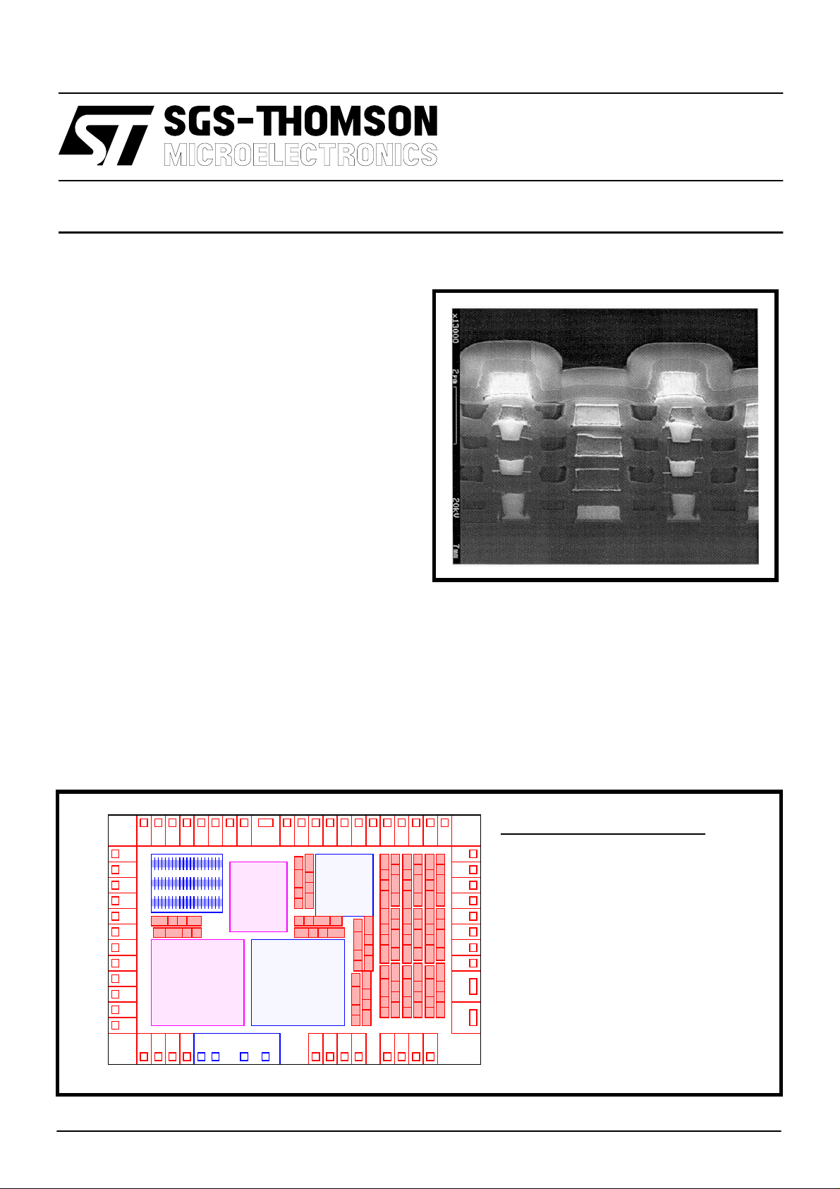
Figure 1
Process Overview
optimum solution for today’s complex system
problems of drive levels and specialized interface
standards.
The product offers a variable bonding approach
supporting pad spacings from 80µ upwards and
supports staggered pad rows to address today’s
bonding technologies. Additional flexibility to
support 65µ and 50µ pad spacing will be
available in the near future.
The I/O can be configured for circuits ranging
from low voltage CMOS and TTL to low swing
differential circuits (LVDS) and the 1Gigabit per
second high speed link. Standards like SCSI, 3.3
and 5 Volt PCI and other 5.0 Volt interfaces are
currently being addressed.
Metal 3 : Al-Cu
Metal 5 : Al-Cu
Metal 4 : Al-Cu
Metal 2 : Al-Cu
Metal 1 : W
2/16
CB45000 SERIES
TECHNOLOGY OVERVIEW
A major feature of the HCMOS6 process is
salicided active areas. This results in source
drain areas that are on the order of one to two
ohms resistance as opposed to the hundreds or
thousands of ohms of source drain resistance in
non-salicided technologies. This very low
resistance is one reason that very low transistor
widths could be utilized in the cell design since
drive is not lost due to source drain resistance.
This use of low width transistors results in lower
capacitance loading of the gates due to the
smaller areas utilized. Low resistance, low
capacitance, and small gates results in low power
usage for inverters as compared to previous
technologies. The reduction in power
consumption allows the usage of salicided active
stripes to distribute power internally to the simple
cell, replacing, in some cases, the usage of the
first metal layer. This saves silicon area by
allowing greater density, permeability and
routability of the cells resulting in greater overall
circuit density.
The other major feature of the HCMOS6 process
is five metal layer interconnect using CMP
(Chemical Mechanical Polishing) planarization.
The use of CMP for improved planar ity between
metal layers allows the use of additional
interconnect layers without yield degradation,
improving density whilst retaining low costs.
The power distribution methodology provides
separate internal distributions to improve product
noise margin and reduce power loss. The three
supplies are:
■ Internal Vdd and Vss
Serves the core cells and the prebuffer sections of the I/O
■ External Vdd and Vss
Serves the output transistors only
■ Receiver Vdd and Vss
Serves the first stages of the receiver cells.
Optional distributions for 5.0V interface and other
standards can be utilized as necessary.
3/16
CB45000 SERIES
10 Ê
LIBRARY
The CB45000 Series library is organized into four
categories:
■ SSI cell library
■ IO Cell library
■ Macrofunctions
■ Module generators
SSI CELL LIBRARY OVERVIEW
The design of the CB45000 family has been
optimized to allow extremely high density, high
speed and low power designs. For these reasons
a wide range of cells with different ranges of
driving capability are available in the library.
The library cells have been optimized in term of
functional and electrical parameters in order to
have:
■ Good balancing
■ Maximum speed
■ Optimum Threshold voltage
m
■ Symmetric Vdd/Vss Noise margin
■ Minimum Power-Speed figure
The geometrical aspect of the cells was
configured to allow extremely dense design, fully
exploiting the features of the Place and Route
tool in terms of horizontal and vertical routing
grids. For Place and Route, up to five levels of
metal are utilized. Intracell wiring is limited as far
as possible to first metal, with second, third and
fourth metal levels dedicated to interconnect
wiring and power distribution. The fifth metal is
used for power and clock bussing.
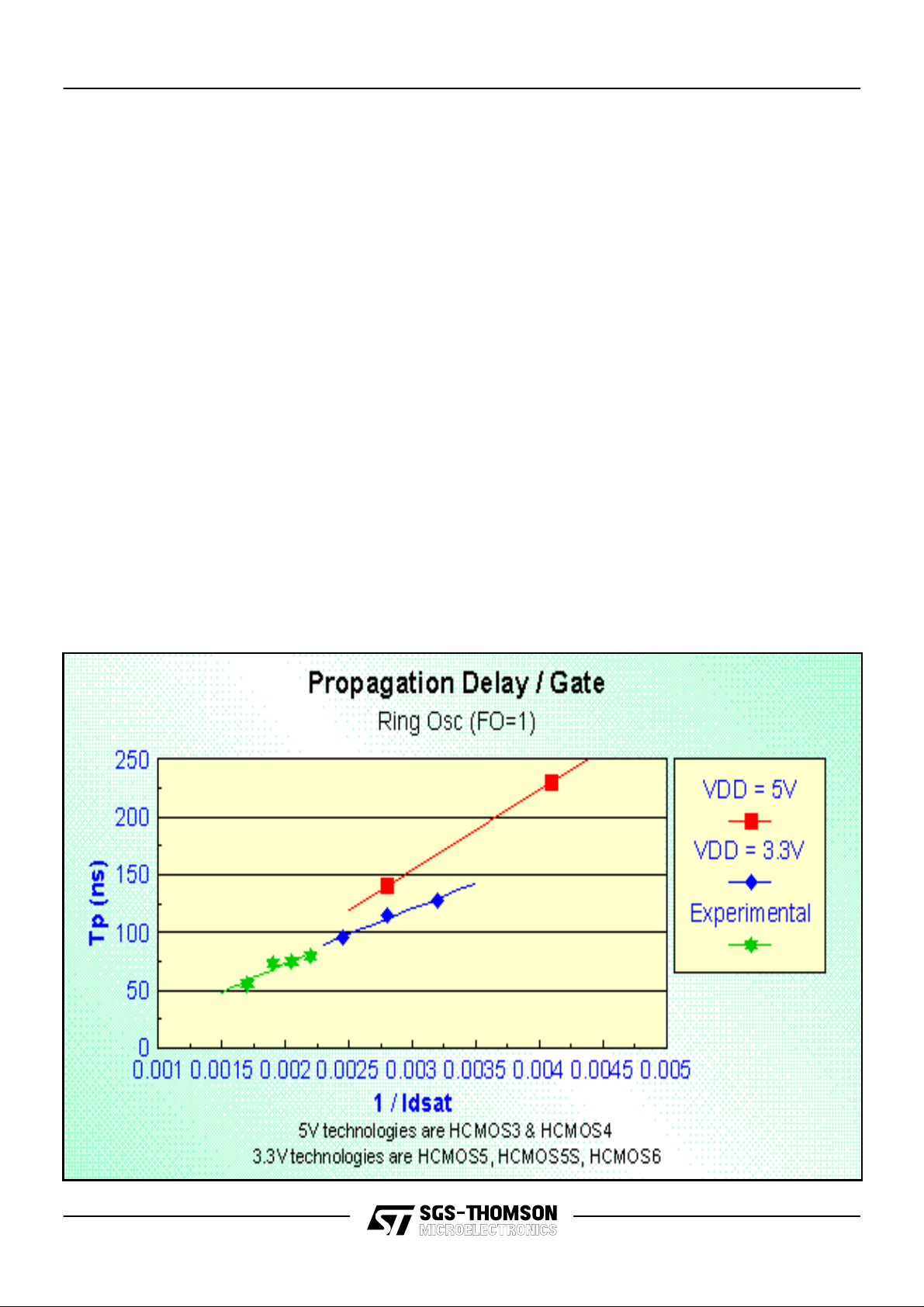
CORE LOGIC
The propagation delays shown in the CB45000
data book are given for nominal processing, 3.3V
operation, and 25 C temperature conditions.
However there are additional factors that affect
the delay characteristics of the macrocells. These
include loading due to fanout and interconnect
routing, voltage supply, junction temperature of
the device, processing tolerance and input signal
transition time.
Prior to physical layout, the design system can
estimate the delays associated with any critical
path. The impact of the placement and routing
can be accurately RC back annotated from the
layout for final simulations of critical timing. The
effects of junction temperature, (K
) and voltage
T
supply (KV) on the delay numbers are
summarized in Table 2 and Table 2. A third factor,
is associated with process variation. This
multiplier has a minimum of 0.8 and a maximum
of 1.2.
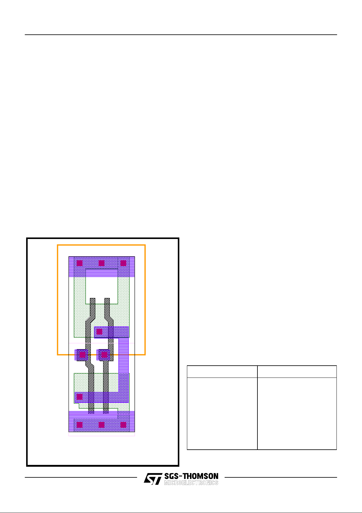
Figure 2. ND2 Core Cell
4/16
Table 1 Junction Temperature Multipliers
TemperatureoCK
T
-55 0.77
-40 0.83
25 1.00
70 1.13
85 1.17
125 1.27
CB45000 SERIES
Table 2 Voltage Multipliers
V
DD
K
V
2.7 1.20
3.0 1.11
3.3 1.00
3.6 0.94
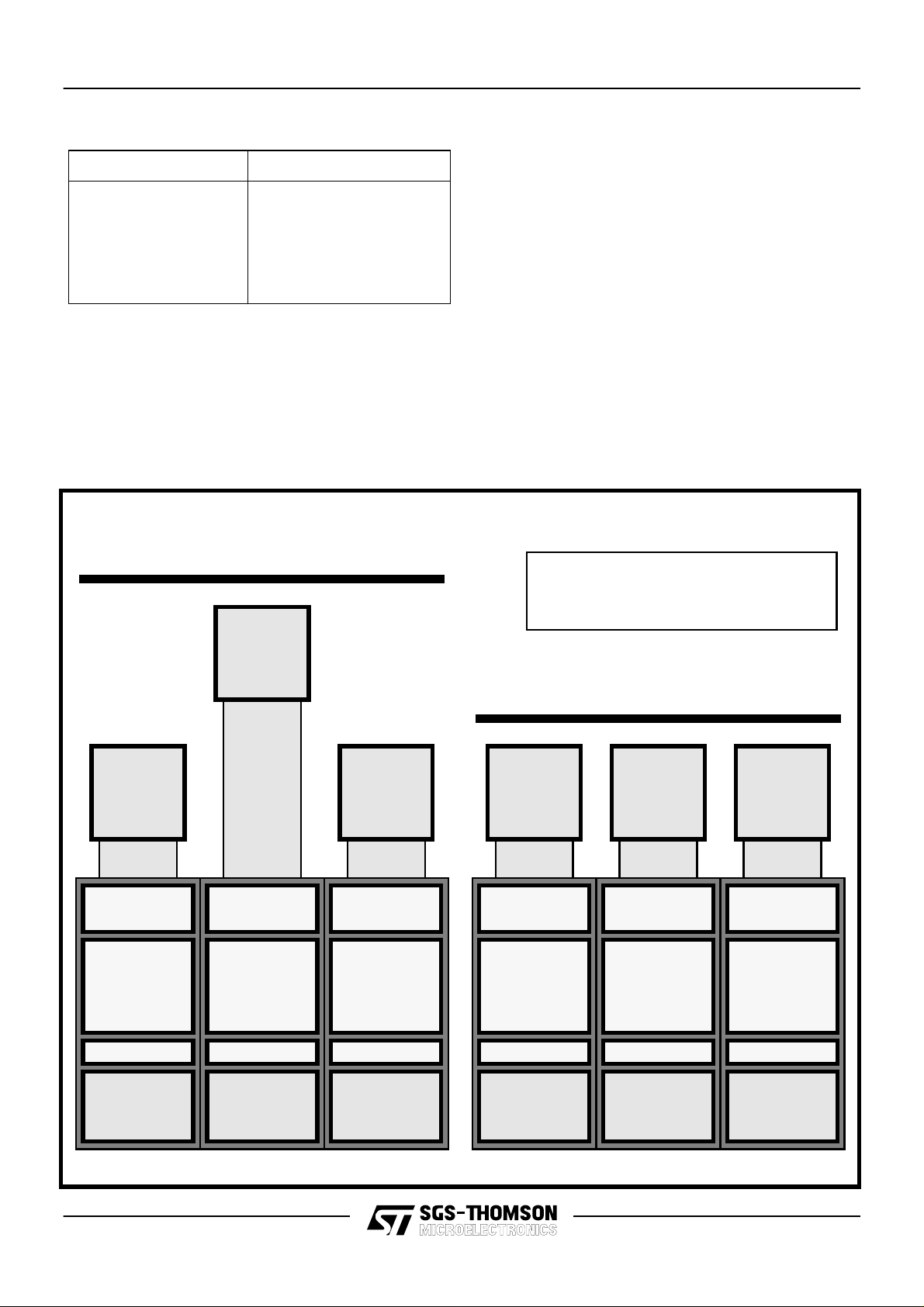
I/O BUFFER LIBRARY
The CB45000 does not use traditional I/O cell
design; SGS-THOMSON was one of the pioneers
of the emerging “Flexible I/O” approach and the
CB45000 features variable bonding and a flexible
output transistor scheme based on a predefined
Figure 3
Flexible IO Buffer Technology
EDGE OF DIE
GUARDRING
set of I/O transistor subcells.
These subcells can be quickly configured using
metallization layers to confor m to a variety of I/O
specifications whilst maintaining optimal ESD
protection levels and latch-up prevention
characteristics.
The I/O circuitry also includes subcells of
specialized transistors that are used to form the
slew rate control sections of each I/O line.
Current spike suppression logic ensures that
conducting transistors are turned off before the
opposing set are turned on.
The bond pad itself is variable in terms of pitch
and size and even supports staggered bonding
methodologies. This is becoming far more
Programmable pad locations allows
one IO cell library to be used for both
staggered and linear bonding.
ESD CLAMP
STRUCTURES
OUTPUT
DRIVE
TRANSISTORS
DIODES
LOGIC CIRCUITS
TEST INTERFACE
SLEW CONTROL
ESD CLAMP
STRUCTURES
OUTPUT
DRIVE
TRANSISTORS
DIODES
LOGIC CIRCUITS
TEST INTERFACE
SLEW CONTROL
ESD CLAMP
STRUCTURES
OUTPUT
DRIVE
TRANSISTORS
DIODES
LOGIC CIRCUITS
TEST INTERFACE
SLEW CONTROL
ESD CLAMP
STRUCTURES
OUTPUT
DRIVE
TRANSISTORS
DIODES
LOGIC CIRCUITS
TEST INTERFACE
SLEW CONTROL
EDGE OF DIE
GUARDRING
ESD CLAMP
STRUCTURES
OUTPUT
DRIVE
TRANSISTORS
DIODES
LOGIC CIRCUITS
TEST INTERFACE
SLEW CONTROL
ESD CLAMP
STRUCTURES
OUTPUT
DRIVE
TRANSISTORS
DIODES
LOGIC CIRCUITS
TEST INTERFACE
SLEW CONTROL
DIE CORE
DIE CORE
5/16

CB45000 SERIES
important as the packaging options become ever
broader.
The pad size and pitch are not determined until
the customers choice of packaging, signal
interface standards and I/O count is considered.
Wire bond pad spacings down to 65µ and 50µ
centres will released in the near future to support
large signal counts without die area loss.
All pads except the sixteen corner pads can be
configured as power or I/O pads. The configured
power pads are known as placeable pads and
have an associated current handling capability.
Their placement is dependent on the types of
output buffers used in the design. For rules
governing the placement of pads, please contact
your local SGS-THOMSON design centre.
Table 3 I/O Drive Capacity for LVCMOS and
LVTTL Slew Rate Buffers
Current Drive
(mA)
Maximum
Capacitance (pF)
2.0 50
4.0 100
8.0 200
I/O TEST INTERFACE
The IO cells have a dedicated test interface to
facilitate parametric and Iddq testing of devices.
This test interface connects standard core signals
or dedicated test signals to the IO cells allowing
all Output Buffers to be driven high, low or put
into tristate regardless of the state of the internal
logic.
This greatly simplifies parametric testing of the
part and also assisting customers who wish to
use this feature during board testing. Note that all
output buffers can be tristated by this function
including buffers that normally do not tristate.
This test function also turns off all pull up or down
devices and shuts down all differential receivers
and converts them into standard CMOS
receivers. This allows Iddq test methodologies to
be employed in a very efficient way, avoiding
unneeded circuit overhead.
Inside the IO cell is a section of specialized
transistors used to create the receiver functions.
A full set of standard receivers with pull up and
pull down devices is present in the library. The
technologies supported match the output buffer
capabilities and include, LVCMOS, LVTTL, GTL,
CTL, Differential, etc. and a five volt interface
capability.
12.0 300
16.0 400
Table 4 I/O Drive Capacity for LVCMOS and
LVTTL Non Slew Rate Buffers
Current Drive
(mA)
Maximum
Capacitance (pF)
2.0 50
4.0 100
8.0 200
12.0 300
16.0 400
6/16
MACROCELLS AND MACROFUNCTIONS
The CB45000 series has internal macrocells that
are robust in variety and performance. The cell
selection has been driven by the need of
Synthesis and HDL based design techniques.
This offering is rich in buffers, complex
combinatorial cells and multi power drive cells,
which allow the Synthesis tool to create a netlist
compatible with the requirements of Place and
Route tools.
Macrofunctions are a series of soft-macros
facilitating quick capture of large functional b loc ks
and are available for such functions as counters,
shift register and adders. Macrofunctions are
implemented at layout by utilizing macrocells and
interconnecting to create the logic function.

Table 5 Module Generator Library
Cell Description
SPRAM
DPRAM
ROM
MODULE GENERATORS
CB45000 SERIES
256K bits max
16K word max 128 bit max
Zero static current, Tristate outputs
256K bits max
16K word max 128 bit max
Zero static current, Tristate outputs
2M bits max
32K word max 64 bit max
Diffusion programmable, Tristate outputs
A series of module generators using compiled
cell generation techniques, are available to
support a range of megacells. These modules
enable the designer to choose individual
parameters in order to create a compiled cell,
which meets the specific application
requirements. These include single port RAM,
dual port RAM and ROM.
The compiled cell generators construct custom
cells, which are implemented using a special leaf
cell technique, ensuring predictable layout and
accurate module characteristics. In choosing
megacells the designer can consider the tradeoffs between speed and area to generate a fully
customized cell which meets their specific device
requirements.
MEGACELLS
These megacell generators are complemented
by a group of application specific embedded
megacells. These allow access to technologies
that have been hitherto the domain of standard
products. Examples include mixed mode cells for
graphics, DAC/ADC’s (4-9 bit), PLL applications,
and Digital Signal Processor functions for cellular
comms, fax and high-speed modems, which
initially consist of a Triple 8-bit DAC, Graphics
RAM, Clock Multiplier PLL and Frequency
Synthesis PLL.
100 Mbps serial transputer links coupled with
large and fast memory can be used for pipelining,
caching and synchro circuits in modern RISC
computing architectures. Viterbi and Reed
Solomon cores aim at the HDTV and satellite
transmission markets. To support telecom needs
for CCITT standard applications, ADPCM cells
supporting CT2 protocol have been developed.
DESIGN FOR TESTABILITY
The time and cost for ASIC testing increases
exponentially as the complexity and size of the
ASIC grows. Using a design for testability
methodology allows large, more complex ASICs
to be efficiently and economically tested.
CB45000 supports the JTAG boundary Scan and
both edge and level sensitive scan design
techniques by providing the necessary
macrocells. Scan testing aids device testability by
permitting access to internal nodes without
requiring a separate external connection for each
node accessed. Testability is assured at device
level with the close coupling of LSSD latch
elements, Automatic Test Pattern Generation
(ATPG) and high pattern depth tester
architecture. BIST options for memory generators
are also available.
At system level, SGS-THOMSON fully supports
IEEE 1149.1, and the I/O structure utilized in this
family is completely compatible. Several types of
core scan cells are provided in the CB45000
Series library. Examples include FDxS/FJKxS
cells which are edge sensitive and LSxx cells
7/16

CB45000 SERIES
which are true LSSD cells. Non-overlapping clock
generator macros are also available.
For parametric and Iddq testing, the I/O cells
contain a dedicated test interface as described
previously (See “I/O TEST INTERFACE” on
page 6.)
Figure 5
Evaluation Device Cross Section
EVALUATION DEVICE
An evaluation device is used to demonstrate the
performance of the CB45000 series as well as
verify the effectiv eness of the design system. The
device has path delays, latches and a set of
macrocells and memory functions which were
used to verify the simulated characteristics that
are supplied in the data book. Characterization of
the path delays including interconnect shows
typical delays of 160 ps for a 2 input NAND with
receivers/drivers operating at frequencies of 200
MHz. The evaluation device is available in a 208
pin plastic quad flat pack.
8/16

CB45000 SERIES
PACKAGE AVAILABILITY
The CB45000 Series is designed to be
compatible with QFP, BGA and SBC package
types, in addition to the more traditional types
found.
The options include Plastic Leaded Chip Carriers
(PLCC) up to 84 pins, while the Metric Quad Flat
Pack (xQFP) offering ranges up to 208 pins. Both
high performance and high power variants are
available as well as the TQFP thin types.
Figure 6
Packaging Capability
NUMBER
OF LEADS
PQFP TQFP BGA PLCC POWER PQFP
(Pins)
20
28
44
64
❍❍
❍❍
68
80
❍❍
84
100
120
128
144
160
176
❍❍
❍❍
❍❍
❍❍ ❍
❍❍
❍
180
208
❍❍
224
225
256
257
304
352
400
480
Ball Grid Array (BGA) packages are available
from 160 to 500 pins with further developments
planned in the near future. SBC types allow the
pin count to reach the area of 1000 pins.
The diversity in pin count and package style giv es
the designer the opportunity to find the best
compromise for system size, cost and
performance requirements.
PACKAGE NAME
Slug/Spreader
❍
❍
❍
❍
❍
❍
✮
✮
✮
❍ Packages in Production
✮ Packages in Development
9/16

CB45000 SERIES
DESIGN ENVIRONMENT
Several interface levels are possible between
SGS-THOMSON and the customer in the
undertaking of an ASIC design. The four levels of
interface are shown in Figure 7. Level 1 is
characterized by SGS-THOMSON receiving the
system specification and taking the design
through to validation and fabrication. At level 2
interface the designer supplies a complete logic
design implemented in a standard generic logic
family. SGS-THOMSON then takes the design
through to layout, validation and fabrication.
Level 3 is the most common and preferred
interface level. Logic capture and pre-layout
simulation are performed by the designer using
an SGS-THOMSON supported design kit. The
design is then taken through layout, validation
and fabrication by SGS-THOMSON.
The SGS-THOMSON design system validates all
designs before fabrication. Design kits are
provided that allow schematic capture entry via
Mentor Graphics and Cadence products.
Simulation is supported for Cadence and Mentor
Graphics. Full support is also provided for
Cadence Verilog, Synopsys VSS and System
Hilo simulators. Figure 8 shows the SGSTHOMSON Design Flow.
Test vector development uses TSSI software
from Summit and Currentest from CrossCheck.
Figure 7
Customer / SGS-THOMSON Interface Levels
SYSTEM SYSTEM
SPECIFICATION
CUSTOMER
LEVEL 1
CUSTOMER
LEVEL 2
LEVEL 3
INTERFACE LEVELS
LEVEL 4
LOGIC
DESIGN
SCHEMATIC
CAPTURE
CUSTOMER
DESIGN
VERIFICATION
CUSTOMER
PRE-LAYOUT
SIMULATION
SGS-THOMSON
SGS-THOMSON
LAYOUT POST-LAYOUT
SIMULATION
SGS-THOMSON
CUSTOMER SGS-THOMSON
MANUFACTURE
AND TEST
SGS-THOMSON
10/16
ECR1 ECR2

Figure 8
SGS-THOMSON Layout Driven Design Flow
CB45000 SERIES
HARDWARE DESCRIPTION
LANGUAGE
VHDL / VERILOG
LOGIC SYNTHESIS
SCAN INSERTION
GATE LEVEL SIMULATION
VERILOG / MENTOR
TIMING ANALYSIS
FORMAL PROOF
ACCELERATION
HW / SW EMULATION
FAULT ANALYSIS
TSSI / IDDQ
FUNCTIONAL
SIMULATION
VHDL / VERILOG
SCHEMATIC CAPTURE
CADENCE
MENTOR
DELAY EVALUATION
RC BACK-ANNOTATION
IPO / ECO
POWER ESTIMATION
POWER ANALYSIS
FLOORPLANNING
CLOCK TREE SYNTHESIS
LAYOUT
SILICON
11/16

CB45000 SERIES
Table 6 Absolute Maximum Ratings (note1)
Supply Voltage, Vdd -0.5 V to + 4.6 V
Input or Output Voltage
5 Volt Tolerant Input or Output Voltage
-0.5 V to (Vdd + 0.5V)
-0.5 V to +6.0 V
DC Forward Bias Current, Input or Output -24mA source, +24mA sink
Storage Temperature Ceramic -65 to 150 degrees Centigrade
Storage Temperature Plastic -40 to 125 degrees Centigrade
ote 1. Referenced to Vss. Stresses above those listed under “absolute Maximum Ratings” may cause permanent damage to the
Note 2. A dedicated 5V extra power supply is needed in case of PCI b uffer usage in order to clip the incoming signal on PCI pads to the
device. This is a stress rating only and functional operation of the device at these or any other conditions above those indicated
in the operation sections of this specification is not implied. Exposure to absolute maximum rating conditions for extended periods may affect the device reliability.
5 Volt tolerant specified Absolute Maximum Rating (5V + Vbe value)R.
Table 7 Recommended DC Operating Conditions
Normal Operating Supply Voltage Vdd (note 1) 3.3 V +/- 10% (3.0 V to 3.6 V)
Extended Operating Supply Voltage Vdd (notes 1,2) 3.3 V + 0.3V/-0.6V (2.7V to 3.6V)
Operating Ambient Temperature
Commercial (note 3)
Industrial (note 3)
Military (note 4)
0 to 70 degrees Centigrade
-40 to +85 degrees Centigrade
-55 to +125 degrees Centigrade
Note 1. Commercial, Industrial, and Military Conditions
Note 2. Low Voltage TTL Circuits are NOT functional to specifications below 3.0 Volts
Note 3. All circuits will operate to full specifications with a Vdd of 3.0V to 3.6V and a junction temperature of -40 to +125 degrees centi-
Note 4. All circuits will be functional from -55 to +150 degrees centigrade junction temperature (military Ambient Temperature Range)
grade. These junction temperatures are compatible with the Commercial and Industrial Temperature Ranges.
but will not necessary operate to published specifications. Only circuits specified as operational to extended temperature range
may be used when operating to Military temperature conditions.
Table 8 General Interface DC Electrical Characteristics (Note 1)
Symbol Parameter Conditions Min Typ Max Unit Notes
Iil Low Level Input Current Vi =Vss +/-10 uA 2
Iih High Level Input Current Vi = Vdd +/-10 uA 2
Ioz Tri-State Output Leakage Vo=0V or Vdd +/-10 uA 2
Cin Input Capacitance Freq=1MHz 2.5 4.0 pF 3,4
Co Output Capacitance Freq=1MHz 4.0 5.5 pF 3,4
Cio Bidi, I/O Capacitance Freq=1MHz 5..0 6.5 pF 3,4
Iklu I/O Latch Up Current V<Vss, V>Vdd 200 500 mA
Vesd Electrostatic Protection HBM 2000 V 5
Note 1. These are extended voltage and temperature specifications
Note 2. Adherence to rules in Power Pin / Pad Specifications Required
Note 3. Excluding Package
Note 4. At 0.0 Volts
Note 5. Human Body Model
Vdd from 2.7 V to 3.6 V ; Temperature Ambient from -55 to 125 degrees Centigrade
12/16

CB45000 SERIES
Table 9 LVTTL Interface DC Electrical Characteristics (Note 1)
Symbol Parameter Conditions Min Typ Max Unit Notes
Vil Low Level Input Voltage 0.8 Volts 2,3
Vih High Level Input Voltage 2.0 Volts 2,3
Vol Low Level Output Voltage Iol = Rated Buffer
0.2 0.4 Volts 2,3,4
Current
Voh High Level Output Voltage Ioh = Rated Buffer
2.4 3.0 Volts 2,3,4
Current
Vt + Schmitt Trigger +Ve
1.7 1.9 Volts 2,3
Threshold
Vt - Schmitt Trigger -Ve
0.9 1.1 Volts 2,3
Threshold
Note 1. These are normal Voltage and extended temperature specifications
Note 2. Adherence to rules in Power Pin / Pad Specifications Required
Note 3. Refer to the CB45000 Standard Cell Specification for full Testing Levels and Conditions
Note 4. Buffers offered in 2, 4, 8 mA TTL options (12, 16 and 24 mA available on request)
Vdd from 3.0 V to 3.6 V
Temperature Ambient from -55 to 125 degrees Centigrade
Table 10 LVCMOS Interface DC Electrical Characteristics (Note 1)
Symbol Parameter Conditions Min Typ Max Unit Notes
Vil Low Level Input Voltage 0.2xVdd Volts 2,3,4
Vih High Level Input Voltage 0.8 x
Vdd
Volts 2,3,4
Vol Low Level Output Voltage Iol = Rated
0.2 0.4 Volts 2,3,4,5,6
Buffer
Current
Voh High Level Output Voltage Ioh = Rated
Buffer
Current
Vt + Schmitt Trigger +Ve
0.85
x
Vdd
0.9
Volts 2,3,4,5,6
x
Vdd
1.7 1.9 Volts 2,3
Threshold
Vt - Schmitt Trigger -Ve
0.9 1.1 Volts 2,3
Threshold
Note 1. These are extended voltage and temperature specifications
Note 2. Adherence to rules in Power Pin / Pad Specifications Required
Note 3. Refer to the CB45000 Standard Cell Specification for full Testing Levels and Conditions
Note 4. Buffers offered in 2, 4, and 8 mA CMOS options
Note 5. Note only one CMOS buffer may sink or source DC current when parametric measurements are taken due to the reason that
Note 6. If no buffers are sinking or sourcing current and all internal pull up or pull down resistors in bidi buffers have been disabled by
Vdd from 2.7 V to 3.6 V
Temperature Ambient from -55 to 125 degrees Centigrade
the power supply specifications for CMOS product are not written to support DC current. If more than one buffer is active voltage drops in the supply may cause false failure readings.
having the T2 Test Pin positive Vol (max) = 0.05 Volts and Voh (min)=Vdd-0.05 Volts
13/16

CB45000 SERIES
Table 11 Five Volt Tolerant Interface DC Electrical Characteristics (Note 1,2)
Symbol Parameter Conditions Min Typ Max Unit Notes
Vil Low Level Input Voltage 0.8 Volts 3,4
Vih High Level Input Voltage 2.0 Volts 3,4
Vol Low Level Output Voltage Iol = Rated Buffer
0.2 0.4 Volts 3,4,5
Current
Voh High Level Output Voltage Ioh = Rated Buffer
2.4 3.0 Volts 3,4,5
Current
Vt + Schmitt Trigger +Ve
1.7 1.9 Volts 3,4
Threshold
Vt - Schmitt Trigger -Ve
0.9 1.1 Volts 3,4
Threshold
Note 1. Five Volt Tolerant Inputs: receivers allowed to receive a 5V signal while being supplied at 3.3V
Note 2. These are normal Voltage and extended temperature specifications
Note 3. Adherence to rules in Power Pin / Pad Specifications Required
Note 4. Refer to the CB45000 Standard Cell Specification for full Testing Levels and Conditions
Note 5. Buffers offered in 3, 4, 6, 8 mA TTL options
Five Volt Tolerant Output: drivers allo w ed to driv e external loads between 0V and 3.3V while being supplied at 3.3V having the
ability to sustain 5V signals when tristated.
TTL specification only; Vdd from 3.0 V to 3.6 V
Temperature Ambient from -55 to 125 degrees Centigrade
14/16

CB45000 SERIES
15/16

DESIGN CENTRES
USA
Carrollton, TX 75006-5039
1310 Electronics Drive
MS 2337
Tel.: (1) 972/466-8844
Lincoln, MA 01773
55 Old Bedford Rd.
Tel.: (1) 617/258-0300
San Jose, CA 95110
2055 Gateway Place
Suite 300
Tel.: (1) 408/452-8585
EUROPE
FRANCE
94253 Gentilly Cedex
7, avenue Gallieni - BP 93
Tel.: (33-1) 47407575
GERMANY
8011 Grasbrunn
Bretonischer Ring 4
Neukeferloh Technopark
Tel.: (49-89) 460060
ITALY
20090 Assago (MI)
Viale Milanofiori
Strade 4 - Palazzo A/4/A
Tel.: (39-2) 89213215
40033 Casalecchio di Reno (BO)
Via R. Fucini, 12
Tel.: (39-51) 591914
SWEDEN
S-16421 Kista
Borgarfjordsgatan, 13
Box 1094
Tel.: (46-8) 7939220
ASIA/PACIFIC
HONG KONG
Wanchai
22nd Floor
Hopewell Centre
183 Queen’s Road East
Tel.: (852-5) 8615788
KOREA
Seoul 121
8th floor Shinwon Building
823-14, Kuksman-Dong
Kang-Nam-Gu
Tel.: (82-2) 553-0399
SINGAPORE
Singapore 2056
28 Ang Mo Kio
Industrial Park 2
Tel.: (65) 482-1411
UNITED KINGDOM and EIRE
Marlow, Bucks SL7 1YL
Planar House, Parkway
Globe Park
Tel.: (44-1628) 890800
Information furnished is believed to be accurate and reliable. However, SGS-THOMSON Microelectronics assumes no
responsibility for the consequences of use of such information nor for any infringements of patents or other rights of third
parties which may result from its use. No license is granted by implication or otherwise under any patent or patent rights
of SGS-THOMSON Microelectronics. Specifications mentioned in this publication are subject to change without notice.
This publication supersedes and replaces all information previously supplied. SGS-THOMSON Microelectronics products are not authorized for use as critical components in life support devices or systems without express written approval
of SGS-THOMSON Microelectronics.
1996 SGS-THOMSON Microelectronics - All rights reserved
SGS-THOMSON Microelectronics GROUP OF COMPANIES
Australia - Brazil - France - Germany - Hong Kong - Italy - Japan - Korea - Malaysia - Malta - Morocco - The Netherlands
- Singapore - Spain - Sweden - Switzerland - Taiwan - United Kingdom - U.S.A.
 Loading...