

HIGH CURR ENT NPN SILICON TRANSISTOR
■ SGS-THOMS O N PREF ERRE D SA LES TYP E
■ NPN TRANSISTOR
■ HIGH CURRENT CAPABILITY
■ FAST SWITCHING SPEED
APPLICATIONS
■ MOTOR CONTROL
■ LINEAR AND SWITCHING INDUSTRIAL
EQUIPMENT
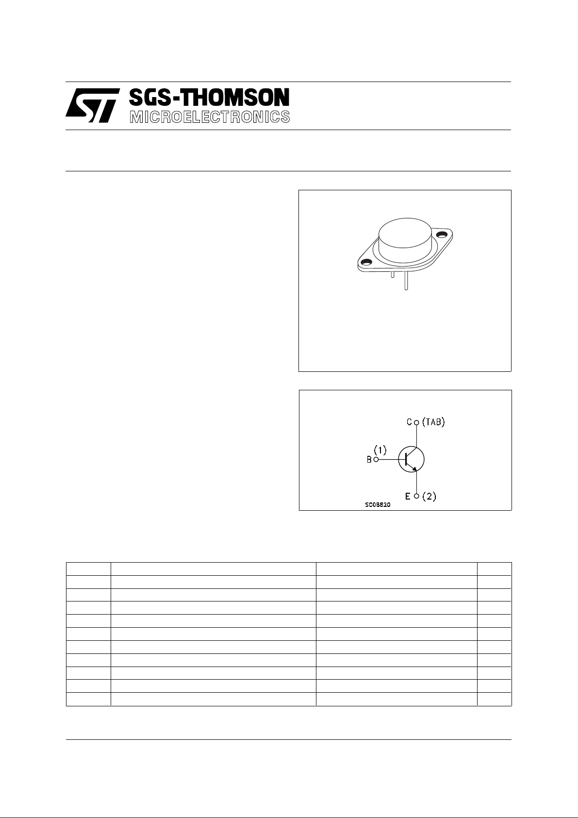
■ HIGH POWER TO-3 PACKAGE
BUX22
1
2
DESCRIPTION
The BUX22 is a silicon multiepitaxial planar NPN
transistor in modified Jedec TO-3 metal case,
TO-3
(version P)
intended for use in switching and linear
applications in military and industrial equipment.
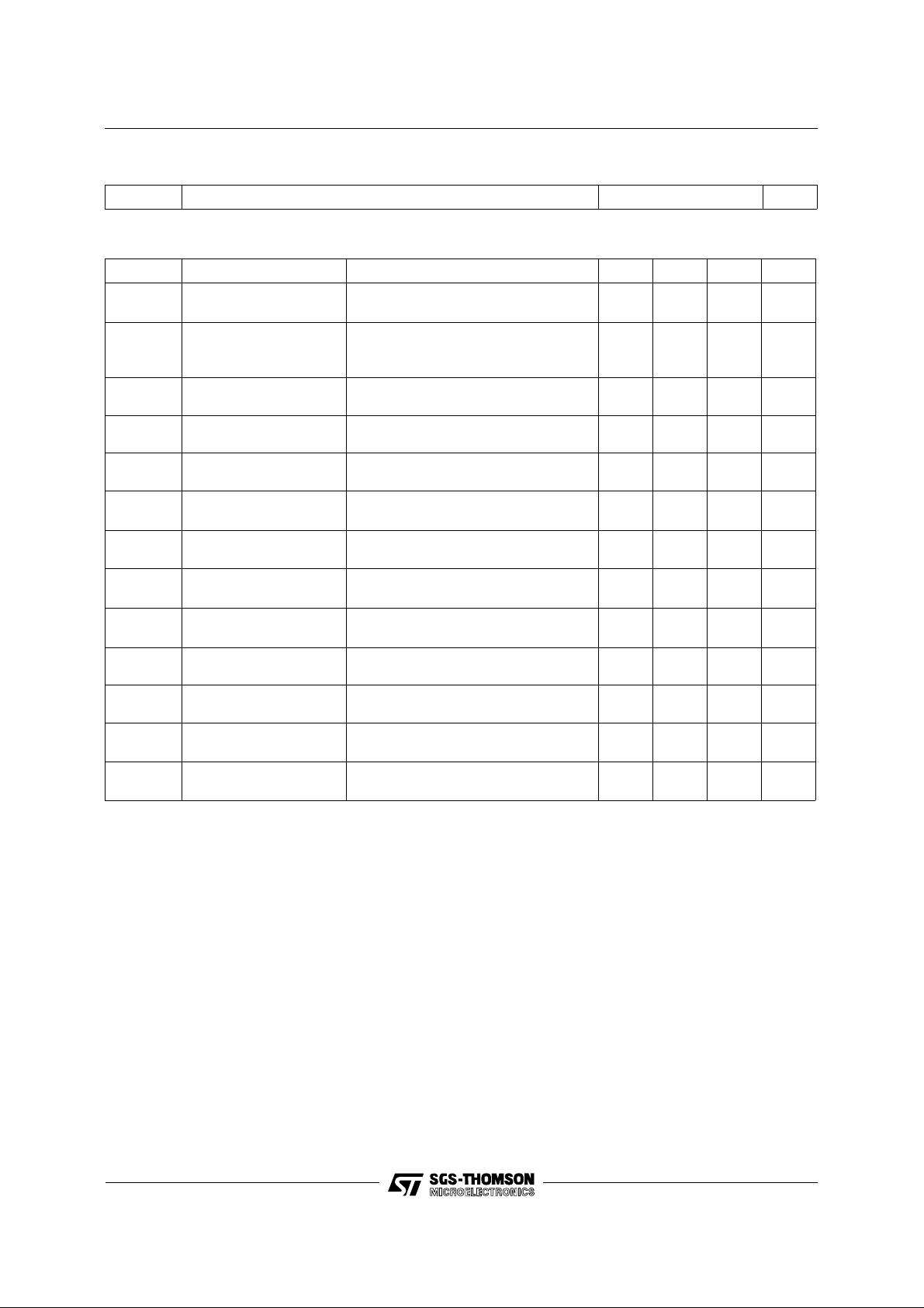
INTERNAL SCHEMATIC DIAGRAM
ABSOL UT E MAXIMU M RATINGS
Symbol Parameter Value Unit
V
V
V
V
I
P
T
Collector-base Voltage (IE = 0) 300 V
CBO
Collector-emitter Voltage (VBE = - 1.5V) 300 V
CEX
Collector-emitter Voltage (IB = 0) 250 V
CEO
Emitter-base Voltage (Ic = 0) 7 V
EBO
Collector Current 40 A
I
C
Collector Peak Current (tp = 10 ms) 50 A
CM
Base Current 8 A
I
B
Total Power Dissipation at T
tot
Storage Temperature -65 to 200
stg
Max Operating Junction Temperature 200
T
j
≤ 25 oC 350 W
case
o
C
o
C
June 1997
1/4
BUX22
THERMAL DATA
R
thj-case
Thermal Resistance Junction-case Max 0.5
o
C/W
ELECTRICAL CHARACTERISTICS (T
= 25 oC unless otherwise specified)
case
Symbol Parameter Test Conditions Min. Typ. Max. Unit
I
CEO
I
CEX
I
EBO
V
CEO(sus)
Collector Cut-off
Current (I
= 0)
B
Collector Cut-off
Current
Emitter Cut-off Current
(I
= 0)
C
∗ Collector-Emitter
= 200 V 3 mA
V
CE
VCE = 300 V VBE = -1.5V
T
= 125 oC
case
V
= 300 V VBE = -1.5V
CE
= 5 V 1 mA
V
EB
3
12
IC = 200 mA 250 V
Sustaining Voltage
V
V
CE(sat)
V
BE(sat)
EBO
Emitter-Base Voltage
(I
= 0)
C
∗ Collector-Emitter
Saturation Voltage
∗ Base-Emitter
= 50 mA 7 V
I
E
IC = 10 A IB = 1 A
I
= 20 A IB = 2.5 A
C
0.2
0.3211.5
IC = 20 A IB = 2.5 A 1.1 1.5 V
Saturation Voltage
h
∗ DC Current Gain IC = 10 A VCE = 4 V
FE
I
S/b
Second Breakdown
Collector Current
f
Transistor Frequency VCE = 15 V IC = 2 A
T
I
= 20 A VCE = 4 V
C
VCE = 140 V t = 1 s
V
= 20 V t = 1 s
CE
20
60
10
0.15
17.5
10 MHz
f = 10 MHz
t
t
∗ Pulsed: Pulse duration = 300µs, duty cycle ≤ 2 %
Turn-on Time IC = 20 A IB1 = 2.5 A
on
Storage Time
s
Fall Time
t
f
Clamped E
Collector Current
s/b
V
= 100 V
CC
IC = 20 A IB1 = 2.5 A
I
= - 2.5 A VCC = 100V
B2
= 250 V
V
clamp
L = 500 µH
0.22 1.3 µs
1.5
0.1720.5
25 A
mA
mA
V
V
A
A
µs
µs
2/4

TO-3 MECHANICAL DATA
BUX22
DIM.
MIN. TYP. MAX. MIN. TYP. MAX.
A 11.00 13.10 0.433 0.516
B 0.97 1.15 0.038 0.045
C 1.50 1.65 0.059 0.065
D 8.32 8.92 0.327 0.351
E 19.00 20.00 0.748 0.787
G 10.70 11.10 0.421 0.437
N 16.50 17.20 0.649 0.677
P 25.00 26.00 0.984 1.023
R 4.00 4.09 0.157 0.161
U 38.50 39.30 1.515 1.547
V 30.00 30.30 1.187 1.193
mm inch
P
A
G
U
V
N
O
B
D
C
E
R
P003F
3/4

BUX22
Information furnished is believed to be accurate and reliable. However, SGS-THOMSON Microelectronics assumes no responsability for the
consequences of use of such information nor for any infringement of patents or other rights of third parties which may results from its use. No
license is granted by implication or ot h erwise under any patent or patent rights of SGS-THOMSON Microelectronics. Specifi cations mentioned
in this publication are subject to change without notice. This publication sup ersedes and replaces all information previously supplied.
SGS-THOMSON Microelectronics products are not authorized for use as critical components in life support devices or systems without express
written approval of SGS-THOMSON Microelectonics.
© 1997 SGS-THOMSON Microelectronics - Printed in Italy - All Rights Reserved
Australia - Brazil - Canada - China - France - Germany - Hong Kong - Italy - Japan - Korea - Malaysia - Malta - Morocco - The Netherlands -
Singapore - Spain - Sweden - Switzerland - Taiwan - Thailand - United Kingdom - U.S.A
SGS-THOMSON Microelectronics GROUP OF COMPANIES
. . .
4/4
 Loading...