

®
HIGH VOLTAGE FAST-SWITCHING
■
STMicroelectronics PREFERRED
SALESTYPE
■
HIGH VOLTAGE CA PA BILIT Y (> 1500 V)
■
VERY HIGH SWITCHING SPEED
APPLICATIONS:
■
HORIZONTAL DEFLECTION FOR HIGH-END
COLOUR TV AND 21" MONITORS
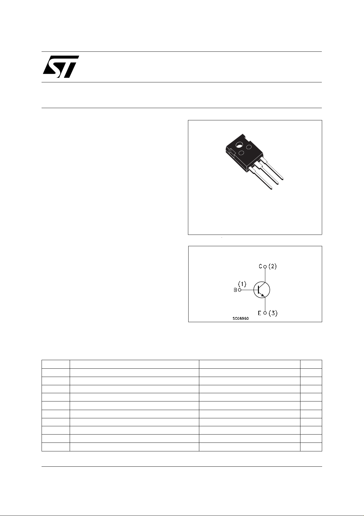
DESCRIPTION
The BUW1215 is manufactured using
Multiepitaxial Mesa technology for cost-effective
high performance and uses a Hollow Emitter
structure to enhance switching speeds.
BUW1215
NPN POWER TRANSISTOR
3
2
1
TO-247
INTERNAL SCHEMATIC DIAGRA M
ABSOLUTE MAXIMUM RATINGS
Symbol Parameter Value Unit
V
V
V
I
I
P
T
Collector-Base Voltage (IE = 0) 1500 V
CBO
Collector-Emitter Voltage (IB = 0) 700 V
CEO
Emitter-Base Voltage (IC = 0) 10 V
EBO
Collector Current 16 A
I
C
Collector Peak Current (tp < 5 ms) 22 A
CM
Base Current 9 A
I
B
Base Peak Current (tp < 5 ms) 12 A
BM
Total Dissipation at Tc = 25 oC200W
tot
Storage Temperature -65 to 150
stg
Max. Operating Junction Temperature 150
T
j
o
C
o
C
February 2002
1/7

BUW1215
THERMAL DATA
R
thj-case
Thermal Resistance Junction-case Max 0.63
o
C/W
ELECTRICAL CHARACT ER ISTI CS
= 25 oC unless otherwise specified)
(T
case
Symbol Parameter Test Conditions Min. Typ. Max. Unit
I
CES
I
EBO
V
CEO(sus)
Collector Cut-off
Current (V
BE
= 0)
Emitter Cut-off Current
(I
= 0)
C
∗ Collector-Emitter
= 1500 V
V
CE
V
= 1500 V Tj = 125 oC
CE
= 5 V 100 µA
V
EB
I
= 100 mA 700 V
C
0.2
2
Sustaining Voltage
(I
= 0)
B
V
EBO
Emitter-Base Voltage
(I
V
∗ Collector-Emitter
CE(sat)
= 0)
C
= 10 mA 10 V
I
E
= 12 A IB = 2.4 A 1.5 V
I
C
Saturation Voltage
V
∗ Base-Emitter
BE(sat)
= 12 A IB = 2.4 A 1.5 V
I
C
Saturation Voltage
h
∗ DC Current Gain I
FE
RESISTIVE LOAD
s
t
f
Storage Time
Fall Time
t
INDUCTIVE LOAD
t
s
t
f
Storage Time
Fall Time
= 12 A VCE = 5 V
C
I
= 12 A VCE = 5 V Tj = 100 oC
C
V
= 400 V IC = 12 A
CC
I
= 2 A I
B1
I
= 12 A f = 31250 Hz
C
I
= 2 A I
B1
V
ceflyback
= 1050 sin
= -6 A 1.5
B2
= -1.5 A
B2
π
6
10
t V
5
7
10 14
5
110
4
220
mA
mA
µs
ns
µs
ns
INDUCTIVE LOAD
s
t
f
Storage Time
Fall Time
t
IC = 6 A f = 64 KHz
I
= 1 A V
B1
V
ceflyback
= 1200 sin
BE(off)
π
5
= -2 A
10
6
t V
* Pulsed: Pulse duration = 300 µs, duty cycle 1.5 %
Safe Operating Area Thermal Impedance
2/7
3.5
180
µs
ns
BUW1215
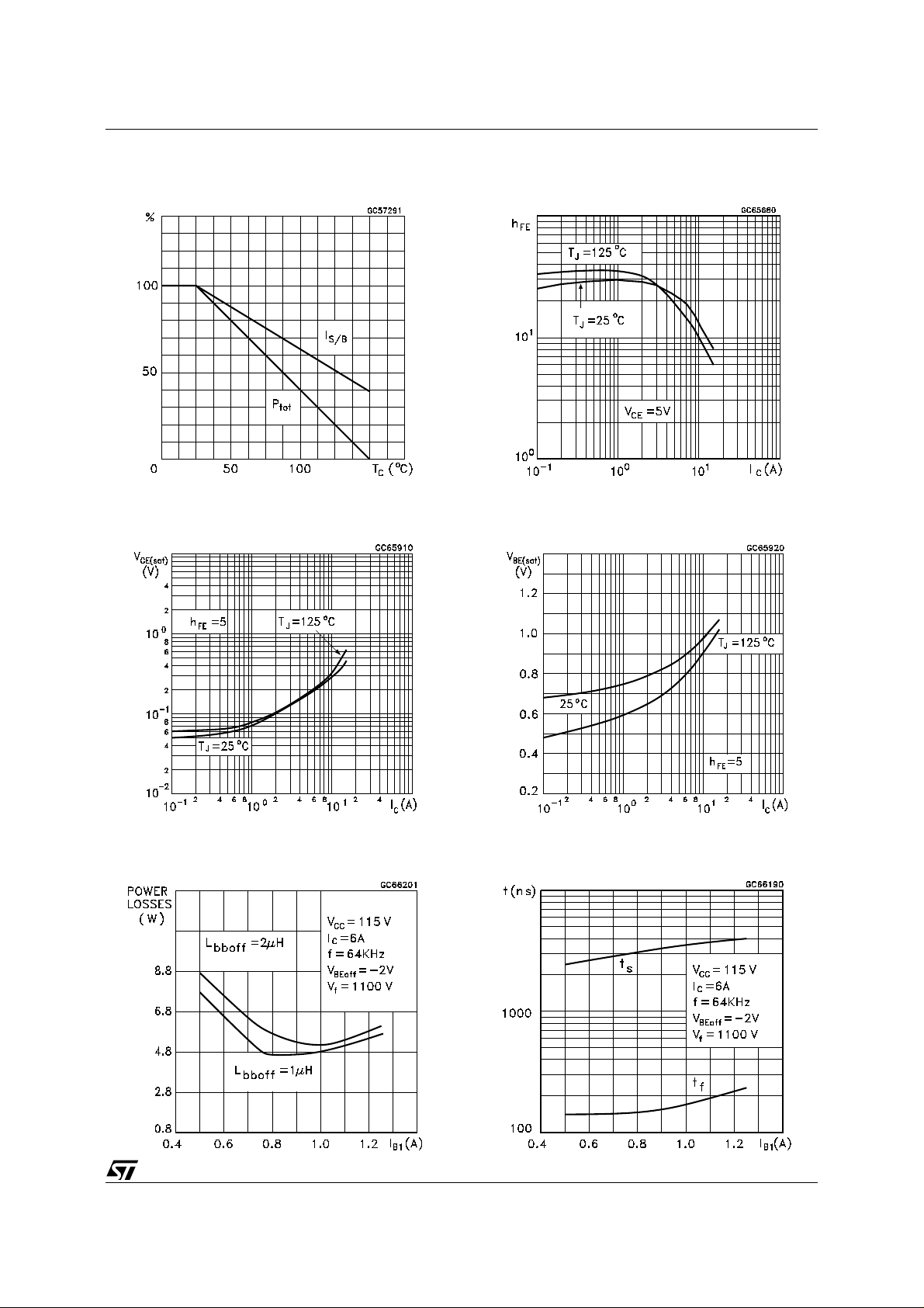
Derating Curve
Collector Emitter Saturation Voltage
DC Current Gain
Base Emitter Saturation Voltage
Power Losses at 64 KHz
Switching Time Inductive Load at 64 KHz
(see figure 2)
3/7
 Loading...