

SGS Thomson Microelectronics BUW1015 Datasheet
®
HIGH VOLTAGE FAST-SWITCHING
■
STMicroelectronics PREFERRED
SALESTYPE
■
HIGH VOLTAGE CA PA BILIT Y (> 1500 V)
■
VERY HIGH SWITCHING SPEED
APPLICATIONS:
■
HORIZONTAL DEFLECTION FOR HIGH-END
COLOUR TV AND 19" MONITORS
DESCRIPTION
The BUW1015 is manufactured using
Multiepitaxial Mesa technology for cost-effective
high performance and uses a Hollow Emitter
structure to enhance switching speeds.
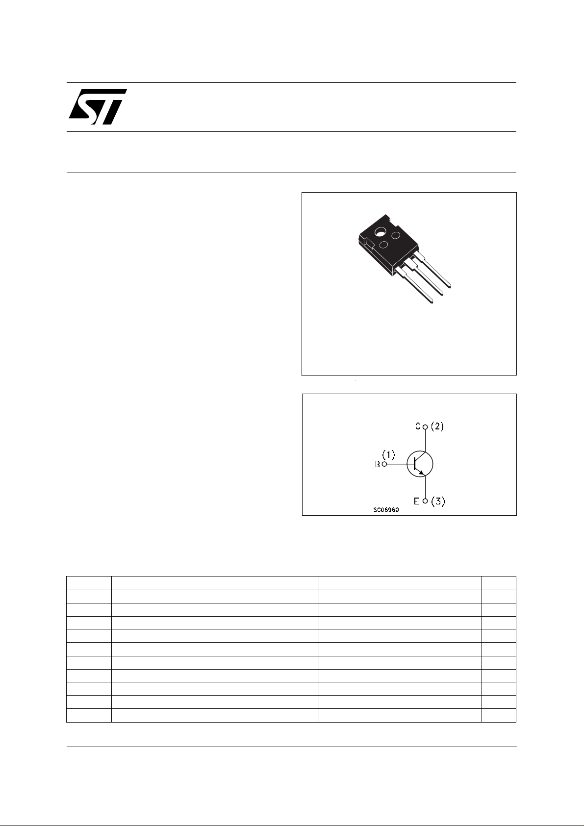
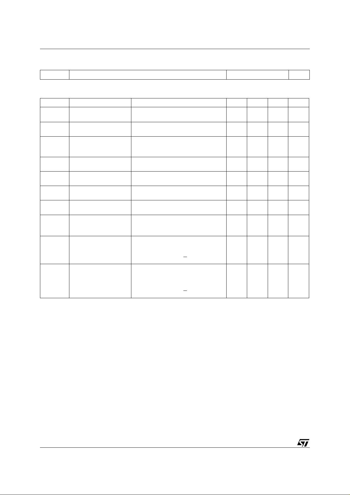
BUW1015
NPN POWER TRANSISTOR
3
2
1
TO-247
INTERNAL SCHEMATIC DIAGRA M
ABSOLUTE MAXIMUM RATINGS
Symbol Parameter Value Unit
V
V
V
I
I
P
T
Collector-Base Voltage (IE = 0) 1500 V
CBO
Collector-Emitter Voltage (IB = 0) 700 V
CEO
Emitter-Base Voltage (IC = 0) 10 V
EBO
Collector Current 14 A
I
C
Collector Peak Current (tp < 5 ms) 18 A
CM
Base Current 8 A
I
B
Base Peak Current (tp < 5 ms) 11 A
BM
Total Dissipation at Tc = 25 oC 160 W
tot
Storage Temperature -65 to 150
stg
Max. Operating Junction Temperature 150
T
j
o
C
o
C
February 2002
1/7
BUW1015
THERMAL DATA
R
thj-case
Thermal Resistance Junction-case Max 0.78
o
C/W
ELECTRICAL CHARACT ER ISTI CS
= 25 oC unless otherwise specified)
(T
case
Symbol Parameter Test Conditions Min. Typ. Max. Unit
I
CES
I
EBO
V
CEO(sus)
Collector Cut-off
Current (V
BE
= 0)
Emitter Cut-off Current
(I
= 0)
C
∗ Collector-Emitter
= 1500 V
V
CE
V
= 1500 V Tj = 125 oC
CE
= 5 V 100 µA
V
EB
I
= 100 mA 700 V
C
0.2
2
Sustaining Voltage
(I
= 0)
B
V
EBO
Emitter-Base Voltage
(I
V
∗ Collector-Emitter
CE(sat)
= 0)
C
= 10 mA 10 V
I
E
= 10 A IB = 2 A 1.5 V
I
C
Saturation Voltage
V
∗ Base-Emitter
BE(sat)
= 10 A IB = 2 A 1.5 V
I
C
Saturation Voltage
h
∗ DC Current Gain I
FE
RESISTIVE LOAD
s
t
f
Storage Time
Fall Time
t
INDUCTIVE LOAD
t
s
t
f
Storage Time
Fall Time
INDUCTIVE LOAD
s
t
f
Storage Time
Fall Time
t
∗
Pulsed: Pulse duration = 300 µs, duty cycle 1.5 %
= 10 A VCE = 5 V
C
I
= 10 A VCE = 5 V Tj = 100 oC
C
V
= 400 V IC = 10 A
CC
I
= 2 A IB2= -6 A 1.5
B1
I
= 10 A f = 31250 Hz
C
I
= 2 A I
B1
V
I
C
I
B1
V
V
= 1200 sin
ceflyback
= 6 A f = 64 KHz
= 1 A
= - 2 V
beoff
= 1100 sin
ceflyback
B2
= -6 A
π
10
5
π
10
5
6
6
t V
t V
7
5
10 14
110
4
220
3.7
200
mA
mA
µs
ns
µs
ns
µs
ns
2/7
BUW1015
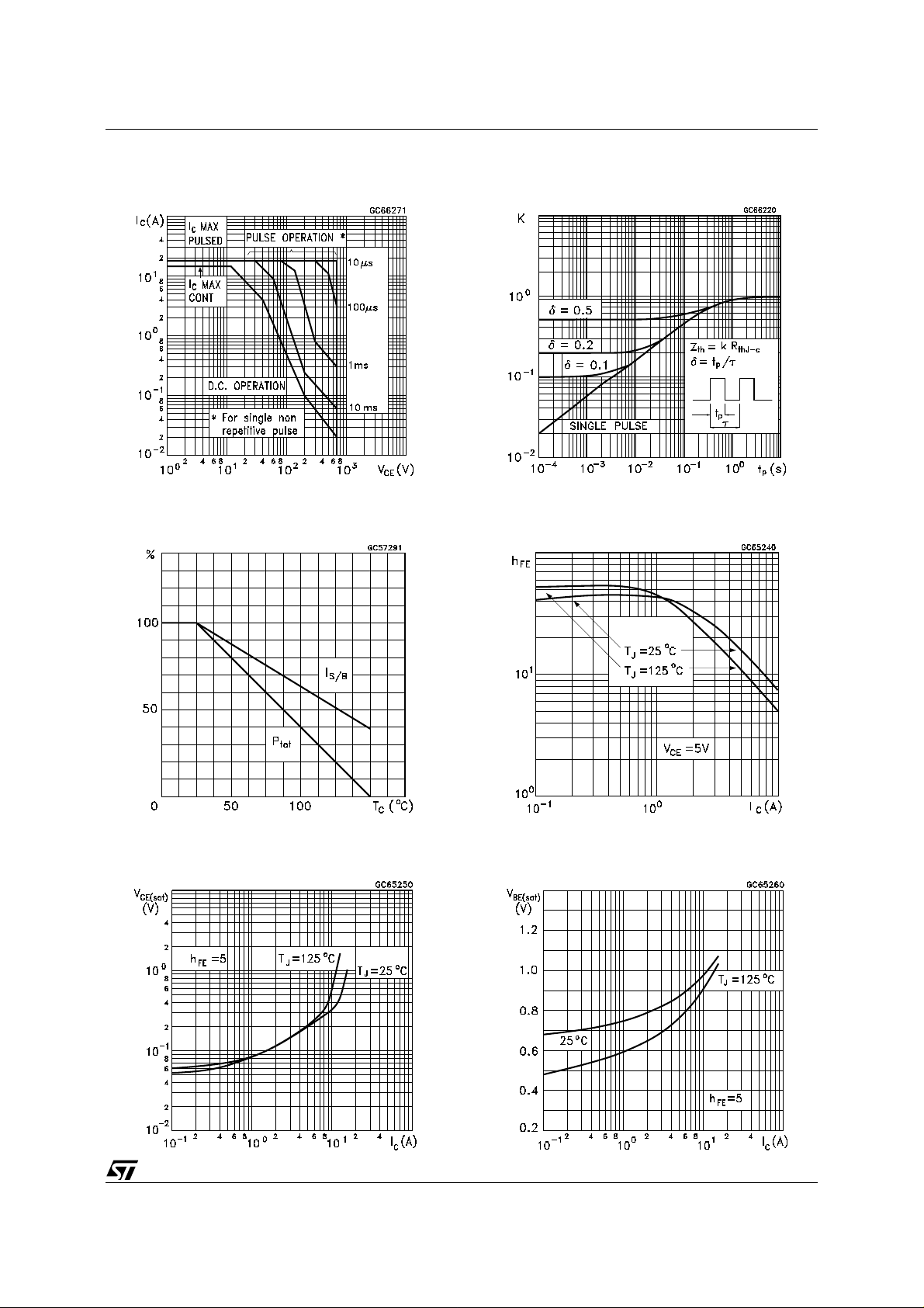
Safe Operating Area
Derating Curve
Thermal Impedance
DC Current Gain
Collector Emitter Saturation Voltage
Base Emitter Saturation Voltage
3/7
 Loading...