

®
■
STMicroelectronics PREFERRED
SALESTYPE
■
NPN TRANSISTOR
■
HIGH CURRENT CAPABILITY
■
FAST SWITCHING SPE ED
■
VERY LOW SATURATION VOLTAGE AND
HIGH GAIN
BUT70W
HIGH POWER NPN TRANSISTOR
APPLICATION
■
SWITCHING REGULATORS
■
MOTOR CONTROL
■
HIGH FREQUENCY AND EFFICENCY
CONVERTERS
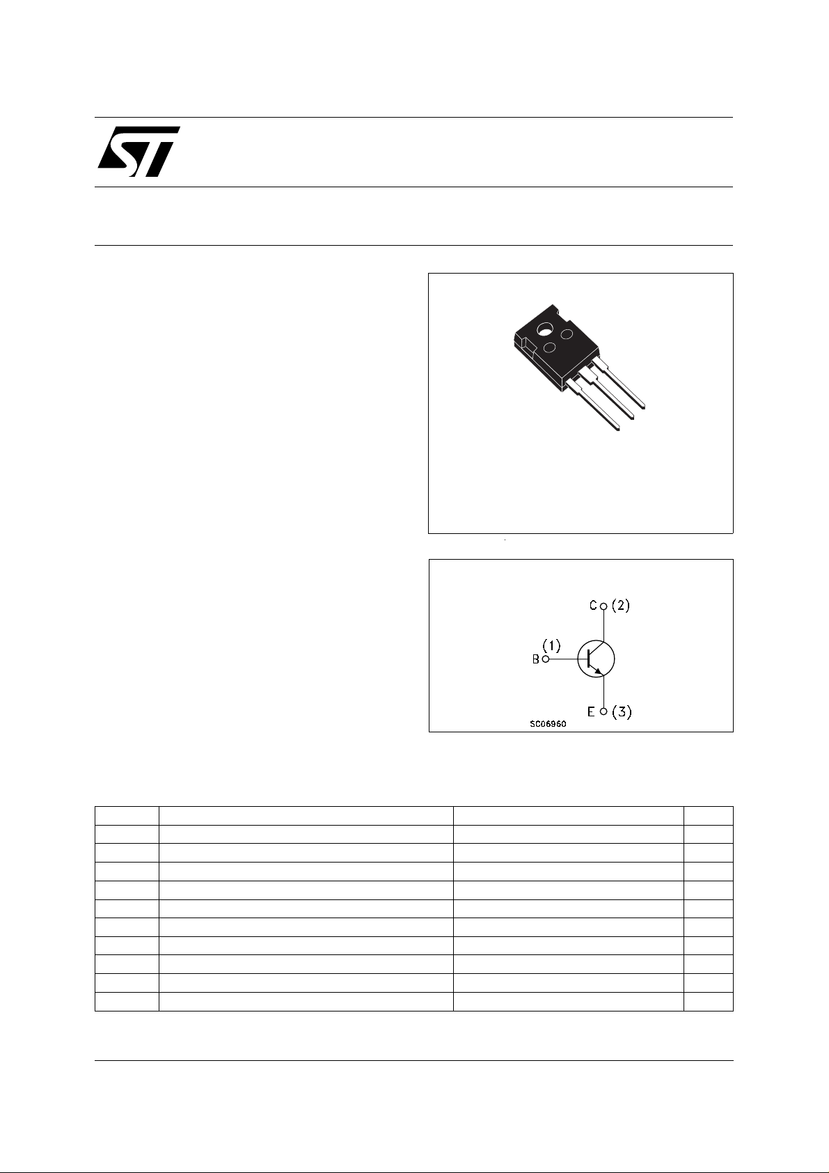
TO-247
3
2
1
DESCRIPTION
The BUT70W is a Multiepitaxial planar NPN
transistor in TO-247 plastic package.
It’s intented for use in high frequency and
efficiency converters such us motor controllers
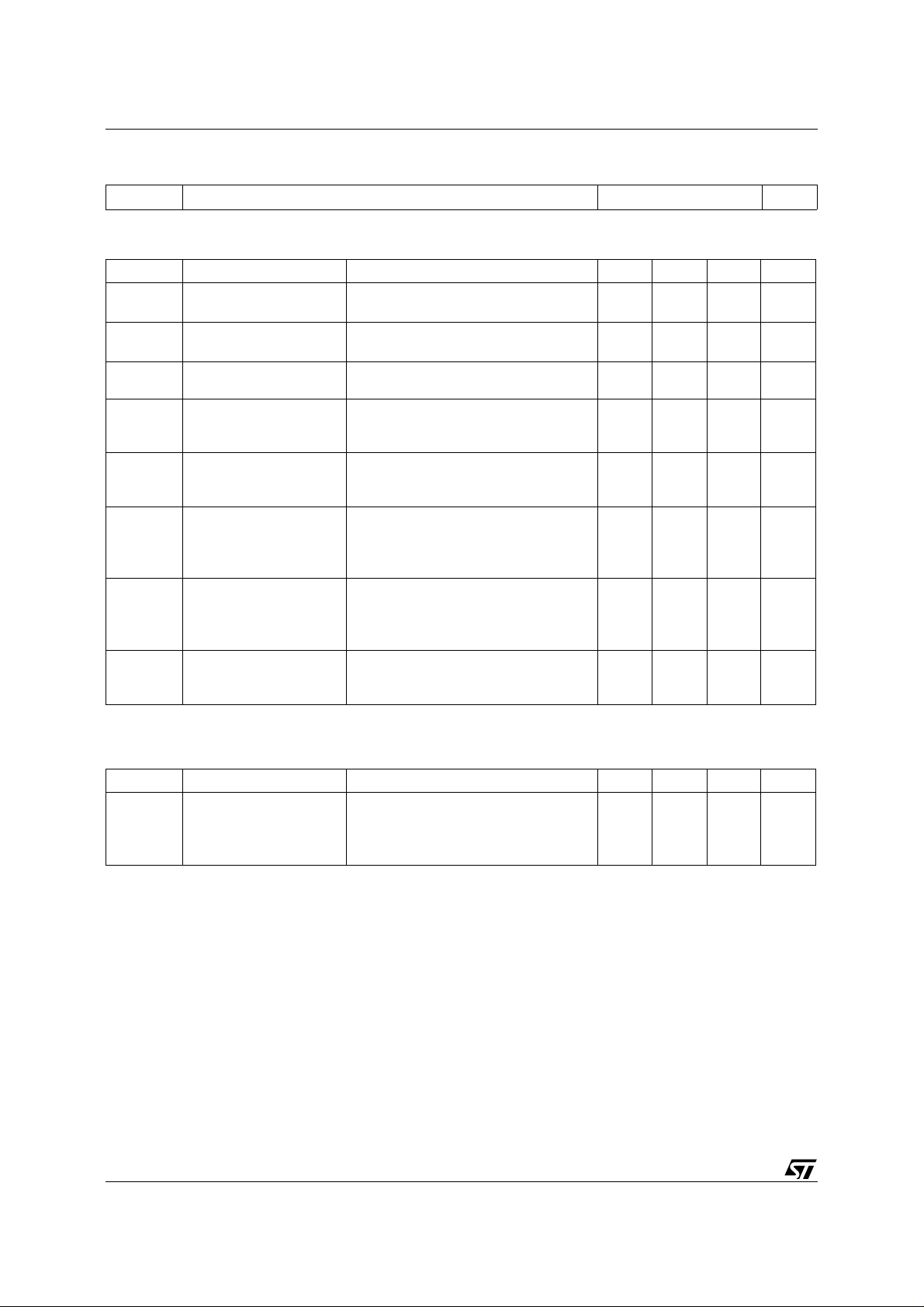
INTERNAL SCHEMATIC DIAGRAM
and industrial equipment.
ABSOLUTE MAXIMUM RATINGS
Symbol Parameter Value Unit
V
V
V
I
E(RMS)
I
I
P
T
Collector-emitter Voltage (VBE = -1.5V) 200 V
CEV
Collector-emitter Voltage (IB = 0) 125 V
CEO
Emitter-Base Voltage (IC = 0) 7 V
EBO
Emitter Current 40 A
Emitter Peak Current 120 A
EM
Base Current 8 A
I
B
Base Peak Current 24 A
BM
Total Power Dissipation at T
tot
Storage Temperature -65 to 150
stg
Max Operating Junction Temperature 150
T
j
case
< 25 oC
200 W
o
C
o
C
February 2002
1/4
BUT70W
THERMAL DATA
R
thj-case
Thermal Resistance Junction-case Max 0.63
o
C/W
ELECTRICAL CHARACTERISTICS
= 25 oC unless otherwise specified)
(T
case
Symbol Parameter Test Conditions Min. Typ. Max. Unit
I
CER
I
CEV
I
EBO
V
CEO(sus)
Collector Cut-off
Current (R
= 5Ω)
BE
Collector Cut-off
Current (V
= -1.5V)
BE
Emitter Cut-off
Current (I
= 0)
C
∗ Collector-Emitter
V
= 200 V
CE
V
= 200 V TC = 100oC
CE
= 200 V
V
CE
V
= 200 V TC = 100oC
CE
= 5 V 1 mA
V
EB
I
= 0.2 A L = 25 mH 125 V
C
1
5
1
4
Sustaining Voltage
(I
= 0)
B
V
(BR)EBO
Emitter-Base
I
= 50 mA 7 V
E
Breakdown Voltage
(I
= 0)
C
V
∗ Collector-Emitter
CE(sat)
Saturation Voltage
V
∗ Base-Emitter
BE(sat)
Saturation Voltage
di
∗ Rated of Rise of
c/dt
on-state Collector
= 70 A IB = 7 A
I
C
I
= 70 A IB = 7 A TC = 100oC
C
I
= 35 A IB = 1.75 A
C
I
= 35 A IB = 1.75 A TC = 100oC
C
= 70 A IB = 7 A
I
C
I
= 70 A IB = 7 A TC = 100oC
C
I
= 35 A IB = 1.75 A
C
I
= 35 A IB = 1.75 A TC = 100oC
C
V
= 100 V RC = 0 IB1 = 3.5 A
CC
= 3 µs TC = 100oC
t
p
140 A/µs
0.9
1.5
0.9
1.2
1.8
1.9
1.4
1.4
Current
∗
Pulsed: Pulse duration = 300 µs, duty cycle < 2 %
mA
mA
mA
mA
V
V
V
V
V
V
V
V
INDUCTIVE LOAD
Symbol Parameter Test Conditions Min. Typ. Max. Unit
1.8
0.2
0.35
2/4
t
t
Storage Time
s
Fall Time
t
f
Cross Over Time
c
IC = 35 A VCC = 90 V
= -5 V RB2 = 1.4 Ω
V
BB
= 1.75 A LC = 0.15 mH
Ι
B1
V
= 125V TC = 100oC
CLAMP
µs
µs
µs
 Loading...