


HIGH VOLTAGE FAST-SWITCHING
■ INTEGRATED ANTIPARALLEL
COLLECTOR- EMITTER DIODE
■ HIGH VOLTAGECAPABILITY
■ LOW SPREADOFDYNAMIC PARAMETERS
■ MINIMUMLOT-TO-LOT SPREADFOR
RELIABLEOPERATION
■ VERYHIGH SWITCHINGSPEED
APPLICATIONS:
■ ELECTRONICBALLASTSFOR
FLUORESCENTLIGHTING
■ FLYBACKAND FORWARDSINGLE
TRANSISTOR LOWPOWER CONVERTERS
DESCRIPTION
The device is manufactured using high voltage
Multi Epitaxial Planar technology for high
switchingspeeds andmediumvoltage capability.
It uses a Cellular Emitter structure with planar
edge termination to enhance switching speeds
while maintainingthe wide RBSOA.
The device is designed for use in lighting
applications and low cost switch-mode power
supplies.
BULD118D-1
NPN POWER TRANSISTOR
3
2
1
IPAK
(TO-251)
INTERNAL SCHEMATIC DIAGRAM
ABSOLUTE MAXIMUM RATINGS
Symb o l Parame t er Val u e Uni t
V
V
V
I
I
P
T
June 1998
Collector-Emitter V oltage (VBE= 0) 700 V
CES
Collector-Emitter V oltage (IB= 0) 400 V
CEO
Emitter-Base V oltage (IC=0) 9 V
EBO
Collect or Current 2 A
I
C
Collect or Peak Cu rr ent (tp<5ms) 4 A
CM
Base Current 1 A
I
B
Base Peak Current (tp<5ms) 2 A
BM
Total Dis sipation at Tc=25oC20W
tot
Stora ge Temperat u re -65 t o 150
stg
Max. O perating Junc t i on Temperat u r e 150
T
j
o
C
o
C
1/7

BULD118D-1
THERMAL DATA
R
thj-case
R
thj-amb
Ther mal Res istance Junctio n-Cas e Max
Thermal Resistance Junction-Ambient Max
6.25
100
o
C/W
o
C/W
ELECTRICAL CHARACTERISTICS (T
=25oC unless otherwise specified)
case
Symbol Parameter Test Cond itions Min. Typ. Max. Unit
I
CES
V
EBO
V
CEO(sus)
Collector C ut-off
Current (V
BE
=0)
=700V
V
CE
V
=700V Tj=125oC
CE
100
500
µA
µA
Emitt er-Base Voltage IE=10mA 9 V
Collector-Emit t er
IC= 100 mA L = 25 mH 400 V
Sust aining Volt ag e
I
CEO
Collector-Emit t er
VCE=400V 250 µA
Leakage Current
V
∗ Collector-Emit t er
CE(sat)
Saturation Voltage
V
∗ Base-Emitt er
BE(sat)
Saturation Voltage
h
∗ DC Cur rent Gain IC=10mA VCE=5V
FE
IC=0.5A IB=0.1A
=1A IB=0.2A
I
C
=2A IB=0.4A
I
C
IC=0.5A IB=0.1A
=1A IB=0.2A
I
C
I
=2A IB=0.4A
C
=0.5A VCE=5V
I
C
=2A VCE=5V
I
C
10
10
0.5
1
1.5
1.0
1.2
1.3
50
8
V
V
V
V
V
V
RESI STIVE LO AD
t
Rise Time
r
t
Fall Time
f
t
s
St orage Time
group A
group B
INDUCTIVE LOAD
t
V
∗
Pulsed: Pulse duration = 300 µs, duty cycle 1.5 %
Note : Productis pre-selected in storage time(GROUP A and GROUP B).SGS-THOMSON reserves the right to ship either groups
according to production availability. Please contact your nearest SGS THOMSON MICROELECTRONICS sales office for delivery details.
St orage Time
s
t
Fall Time
f
Diode Forward Volt age IC = 1 A 2.5 V
F
VCC = 125 V I
=0.4A IB2=-0.2A
I
B1
=30µs
t
p
=2A
C
IC=1A IB1=0.2A
=-5V L=50mH
V
BE
V
clamp
= 300 V
1.4
2
0.7
0.3 0.5
2.1
2.75
0.8
0.10
µs
µs
µs
µs
µs
µs
2/7
BULD118D-1
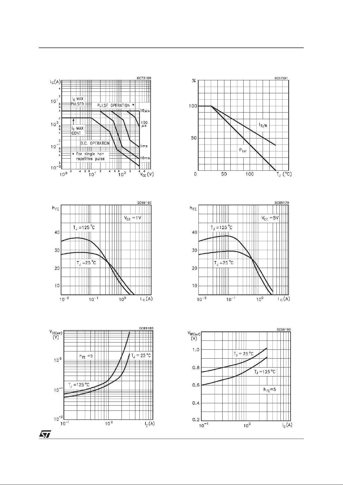
Safe OperatingAreas
DCCurrent Gain
DeratingCurve
DC Current Gain
CollectorEmitter Saturation Voltage
BaseEmitter Saturation Voltage
3/7
 Loading...