

HIGH VOLTAGE FAST-SWITCHING
■ INTEGRATED ANTISATURATIONAND
PROTECTIONNETWORK
■ INTEGRATED ANTIPARALLEL COLLECTOR
EMITTER DIODE
■ HIGH VOLTAGE CAPABILITY
■ LOW SPREADOF DYNAMIC PARAMETERS
■ MINIMUMLOT-TO-LOT SPREAD FOR
RELIABLEOPERATION
■ VERYHIGH SWITCHING SPEED
■ ARCINGTEST SELFPROTECTED
BUL903ED
NPN POWER TRANSISTOR
3
2
1
APPLICATIONS
■ LAMPELECTRONICBALLASTFOR
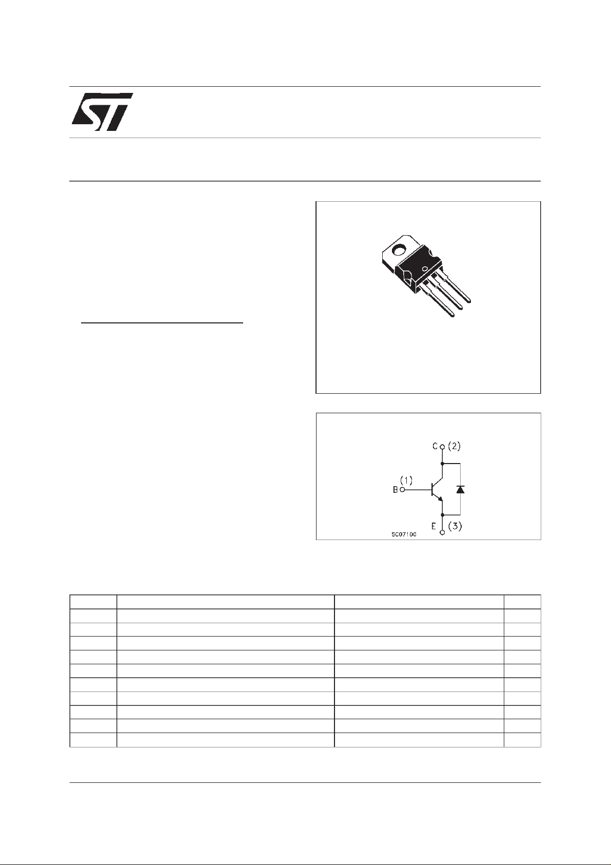
TO-220
FLUORESCENT LIGHTINGUSING 277V
HALF BRIDGECURRENT-FED
CONFIGURATION
DESCRIPTION
The BUL903ED is manufactured using high
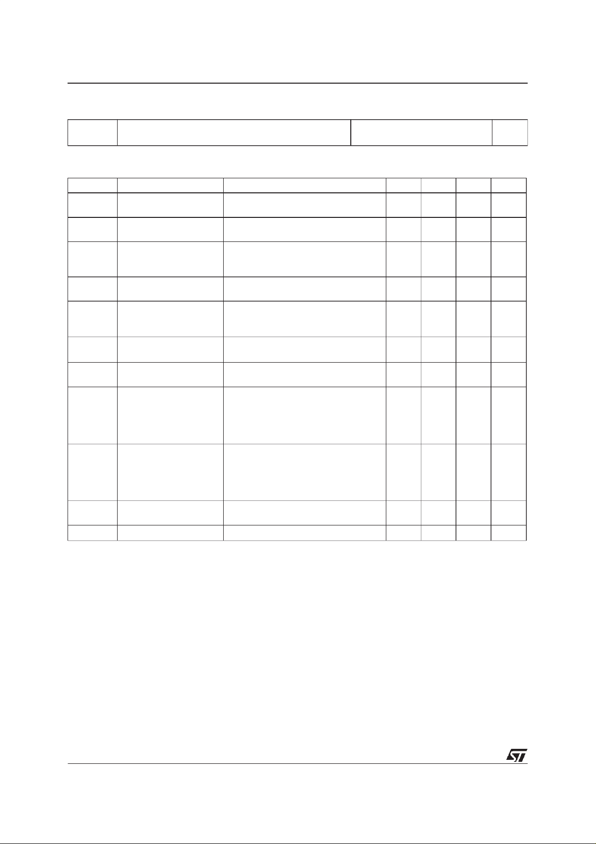
INTERNAL SCHEMATIC DIAGRAM
voltage Multi Epitaxial Planar technologyfor high
switchingspeeds and high voltage capability.
The device has been designed in order to
operate without baker clamp and transil
protection. This enables saving from 2 up to 10
components in the application.
ABSOLUTE MAXIMUM RATINGS
Symb o l Parameter Val u e Uni t
V
V
V
I
I
P
T
Collector-Emitter Voltage (VBE= 0) 900 V
CES
Collect or- E m itter Volta ge (IB = 0) 400 V
CEO
Emitter-Base Voltage ( IC = 0) 7 V
EBO
Collect or Current 5 A
I
C
Collect or Peak Current ( tp<5 ms) 8 A
CM
Base Current 2 A
I
B
Base Peak Current ( tp<5 ms) 4 A
BM
Tot al Dissipa t ion at Tc = 25oC70W
tot
Storage Temperature -65 to 150
stg
Max. Oper ating Junct i on T emperatu re 150
T
j
o
C
o
C
June 1998
1/6
BUL903ED
THERMAL DATA
R
thj-case
R
thj- amb
Ther mal Resistan ce Junct io n- Case Max
Thermal Resistance Junction-Ambient Max
1.8
62.5
o
C/W
o
C/W
ELECTRICAL CHARACTERISTICS (T
=25oC unlessotherwise specified)
case
Symbol Parameter Test Condition s Min. Typ. Max. Unit
I
I
CES
EBO
Collector C ut-off
Current (V
BE
=0)
Base- Emitter Leakage
=900V 1 mA
V
CE
VEB=7V 100 µA
Current
V
CEO(sus)
Collector-Emitt er
I
=10mA L=25mH 400 V
C
Sust aining Volt ag e
=0)
(I
B
V
∗ Collector-Emitt er
CE(sat)
IC=1A IB=0.15A 1.0 V
Saturation Voltage
V
∗ Base-Emitt er
BE(sat )
Saturation Voltage
h
∗ DC Current G ain IC=5mA VCE=10V
FE
V
Parallel Diode Forw ard
F
IC=0.1A IB=0.05A
=0.5A IB=0.1A
I
C
=2.0A IB=0.4A
I
C
=0.5A VCE=3V
I
C
IF=3A 1.2 V
8
20
1.0
1.1
1.2
Volt age
RESI STIVE LOAD
t
t
d
t
r
s
t
f
Delay Time
Rise Tim e
St orage Time
Fall T ime
RESI STIVE LOAD
t
t
T
t
t
d
r
s
f
RR
Delay Time
Rise Tim e
St orage Time
Fall T ime
Diode Rev ers e
Recov ery Tim e
E
∗
Pulsed: Pulse duration = 300 µs, duty cycle 1.5 %
Avalanche E nergy L = 2 mH 6 mJ
sb
VCC=125V IC=0.7A
=0.05A IB2=0.4A
I
B1
=300µs
t
p
VCC=125V IC=0.5A
= 0 . 045 A IB2=0.5A
I
B1
t
=300µs
p
IF=1A di/dt=100A/µs
=30V
V
DD
0.2
1.0
0.8
0.25
0.2
0.5
0.8
0.5
300 ns
V
V
V
µs
µs
µs
µs
µs
µs
µs
µs
2/6

BUL903ED
Safe Operating Areas
DCCurrent Gain
DeratingCurve
DC Current Gain
CollectorEmitter Saturation Voltage
BaseEmitter Saturation Voltage
3/6

BUL903ED
ReverseBiasedSOA
ResistiveLoadSwitching TestCircuit
EnergyRatingTest Circuit
4/6
Vin
Tp
L=2mH
Rg
Vcc
C
T1
TUT
Vbb
+
SC12620

TO-220 MECHANICAL DATA
BUL903ED
DIM.
MIN. TYP. MAX. MIN. TYP. MAX.
A 4.40 4.60 0.173 0.181
C 1.23 1.32 0.048 0.051
D 2.40 2.72 0.094 0.107
D1 1.27 0.050
E 0.49 0.70 0.019 0.027
F 0.61 0.88 0.024 0.034
F1 1.14 1.70 0.044 0.067
F2 1.14 1.70 0.044 0.067
G 4.95 5.15 0.194 0.203
G1 2.4 2.7 0.094 0.106
H2 10.0 10.40 0.393 0.409
L2 16.4 0.645
L4 13.0 14.0 0.511 0.551
L5 2.65 2.95 0.104 0.116
L6 15.25 15.75 0.600 0.620
L7 6.2 6.6 0.244 0.260
L9 3.5 3.93 0.137 0.154
DIA. 3.75 3.85 0.147 0.151
mm inch
P011C
5/6

BUL903ED
Information furnished is believed tobe accurate and reliable. However,STMicroelectronicsassumes no responsibility for theconsequences
of use of such information nor for any infringement of patents or other rights of third parties which may result from its use. No license is
granted by implication orotherwise under any patent or patent rights of STMicroelectronics. Specification mentioned in this publication are
subject tochange withoutnotice. This publication supersedes andreplaces all information previously supplied.STMicroelectronics products
are not authorized for use as critical componentsin life support devices orsystems withoutexpress written approval of STMicroelectronics.
Australia -Brazil - Canada- China - France- Germany - Italy - Japan- Korea- Malaysia -Malta- Mexico - Morocco - TheNetherlands -
Singapore- Spain- Sweden- Switzerland- Taiwan -Thailand - United Kingdom- U.S.A.
The ST logo isa trademarkof STMicroelectronics
1998 STMicroelectronics– Printed in Italy– AllRights Reserved
STMicroelectronicsGROUP OF COMPANIES
.
6/6
 Loading...