


®
MED IUM VOLTAGE FAST -SWITCHING
■
INTEGRATED ANTIPARALL EL
COLLECTOR-EMITTER DIODE
■
LOW SPREAD OF DYNAMIC PARAMETERS
■
MINIMUM LOT-TO-LOT SPREAD FOR
RELIABLE OPERATION
■
VERY HIGH SW ITCHING SPEED
■
HIGH RUGGEDNESS
BUL85D
NPN POWER TRANSISTOR
APPLICATIONS
■
110V AC ELECTRONIC TRANSFO RMERS
FOR HALOGEN LAMPS UP TO 100 W
■
SWITCH MODE POWER SUPPLIES
3
2
1
TO-220
DESCRIPTION
The BUL85D is manufactured using Multi
Epitaxial Planar technology for high switching
speeds and medium voltage capability.
The BUL85D is designed for use in 110V AC
electronic transformers for halogen lamps.
INTERNAL SCHEMATIC DIAGRAM
ABSOLUTE MAXIMUM RATINGS
Symbol Parameter Value Unit
V
V
V
I
I
P
T
Collector-Emitter Voltage (VBE = 0) 500 V
CES
Collector-Emitter Voltage (IB = 0) 250 V
CEO
Emitter-Base Voltage
EBO
I
C
CM
I
B
BM
tot
stg
T
j
= 0, IB < 2.5 A, tp < 10µs, TJ < 150 oC)
(I
C
Collector Current 8 A
Collector Peak Current (tp < 5 ms) 15 A
Base Current 4 A
Base Peak Current (tp < 5 ms) 8 A
Total Dissipation at Tc = 25 oC80W
Storage Temperature -65 to 150
Max. Operating Junction Temperature 150
V
(BR)EBO
V
o
C
o
C
January 2002
1/7
BUL85D
THERMAL DATA
R
thj-case
R
thj-amb
Thermal Resistance Junction-Case Max
Thermal Resistance Junction-Ambient Max
1.56
62.5
o
C/W
o
C/W
ELECTRICAL CHARACTERISTICS
= 25 oC unless otherwise specified)
(T
case
Symbol Parameter Test Conditions Min. Typ. Max. Unit
I
CES
I
EBO
V
(BR)EBO
Collector Cut-off
Current (V
BE
= 0)
Emitter Cut-off Current
(I
= 0)
C
Emitter-Base
= 500 V
V
CE
V
= 500 V Tj = 125 oC
CE
= 9 V 100 µA
V
EB
I
= 10mA 10 18 V
E
100
500
Breakdown Voltage
(I
= 0)
C
V
CEO(sus)
∗ Collector-Emitter
I
= 10 mA L = 25 mH 250 V
C
Sustaining Voltage
(I
= 0)
B
V
∗ Collector-Emitter
CE(sat)
Saturation Voltage
V
∗ Base-Emitter
BE(sat)
Saturation Voltage
h
∗ DC Current Gain I
FE
RESISTIVE LOAD
s
t
f
Storage Time
Fall Time
t
INDUCTIVE LOAD
s
t
f
Storage Time
Fall Time
t
= 2 A IB = 0.4 A
I
C
I
= 4 A IB = 0.8 A
C
I
= 8 A IB = 1.6 A
C
= 2 A IB = 0.4 A
I
C
I
= 8 A IB = 1.6 A
C
= 10 mA VCE = 5 V
C
I
= 0.5 A VCE = 5 V
C
I
= 14 A VCE = 10 V
C
I
= 4 A VCC = 150 V
C
I
= -I
B(on)
≥ 30 µs (see figure 2)
t
p
I
= 4 A V
C
I
= 0.8 A V
B
= 0 Ω tp ≥ 30µs
R
BB
B(off)
= 0.8 A
CL
BE(off)
= 200 V
= -3 V
10
4
1.2 1.8 2.4
0.1 0.3
0.6
1.2
1.1
1.5
60
10
250
0.7
50
(see figure 1)
V
∗
Pulsed: Pulse duration = 300 µs, duty cycle 1.5 %
Diode Forward Voltage IC = 5 A 1.5 V
f
µA
µA
V
V
V
V
V
µs
ns
µs
ns
2/7
BUL85D
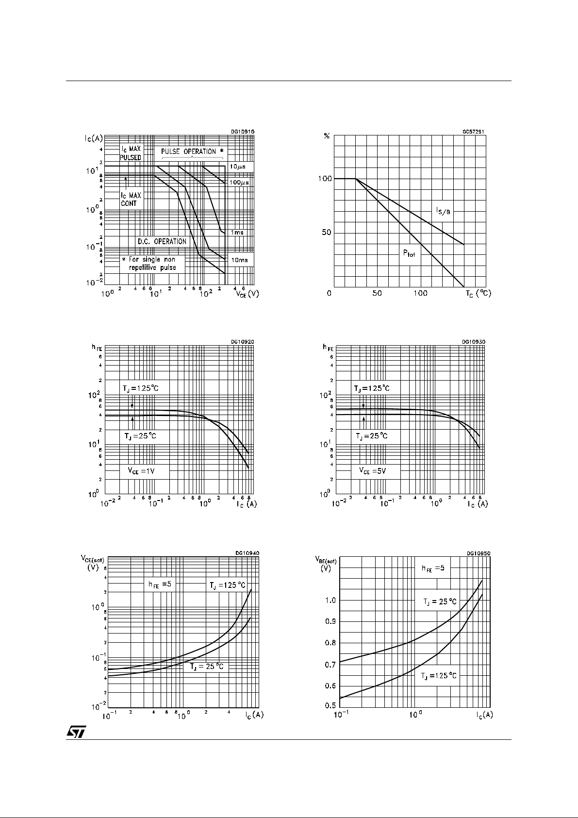
Safe Operating Area
DC Current Gain
Derating Curve
DC Current Gain
Collector Emitter Saturation Voltage
Base Emitter Saturation Voltage
3/7

BUL85D
Switching Time Resistive Load
Diode Forward Voltage
Switching Time Inductive Load
Reverse Biased SOA
4/7

BUL85D
Figure 1:
1) Fast electronic switch
2) Non-inductive Resistor
3) Fast recovery rectifier
Figure 2:
Inductive Load Switching Test Circuit.
Resistive Load Switching Test Circuit.
1) Fast electronic switch
2) Non-inductive Resistor
5/7

BUL85D
TO-220 MECHANICAL DATA
DIM.
A 4.40 4.60 0.173 0.181
C 1.23 1.32 0.048 0.052
D 2.40 2.72 0.094 0.107
E 0.49 0.70 0.019 0.027
F 0.61 0.88 0.024 0.034
F1 1.14 1.70 0.044 0.067
F2 1.14 1.70 0.044 0.067
G 4.95 5.15 0.194 0.202
G1 2.40 2.70 0.094 0.106
H2 10.00 10.40 0.394 0.409
L2 16.40 0.645
L4 13.00 14.00 0.511 0.551
L5 2.65 2.95 0.104 0.116
L6 15.25 15.75 0.600 0.620
L7 6.20 6.60 0.244 0.260
L9 3.50 3.93 0.137 0.154
M 2.60 0.102
DIA. 3.75 3.85 0.147 0.151
MIN. TYP. MAX. MIN. TYP. MAX.
mm inch
6/7
P011CI

BUL85D
Information furnished is believed to be accurate and reliable. However, STMicroelectronics assumes no responsibility for the consequences
of use of such inform ation nor for any in fringe ment o f patents or other rig hts of third par ties wh ich may result from its u se. N o li cen se is
granted by implication or otherwise un der any patent or patent rights of STMicroelectronics. Specification mentioned in this publication are
subject to change without notice. This publication supersedes and replaces all information previously supplied. STMicroelectronics products
are not authorized f or use as critical components in life support devices or systems without express written approval of STMicroelectronics.
The ST logo is a trademark of STMicroelectronics
© 2002 STMicroelectro nics – Printed in Italy – All Rights Reserved
STMicroelectronics GROUP OF COMPANIES
Australia - Brazil - Canada - China - Finland - France - Germany - Hong Kong - India - Israel - Italy - Japan - Malaysia - Malta - Morocco -
Singapore - Spain - Sweden - Switzerland - United Kingdom - United States.
http://www.st.com
7/7
 Loading...