

®
HIGH VOLTAGE FAST-SWITCHING
■ HIGH VOLTAGE CAPABILITY
■ LOW SPREAD OF DYNAMIC PARAMETERS
■ MINIMUM LOT-TO-LO T SPREAD FOR
RELIAB LE OP ERA T ION
■ VERY HIGH SWITCHING SPEED
■ LARGE RBSO A
BUL742
NPN POW ER TRANSISTOR
APPLICATIONS
■ ELECTRONIC BA LLAS T FOR
FLUORESCE NT LIG HT I NG
■ SWITCH MODE PO W E R S UPP LIES
DESCRIPTION
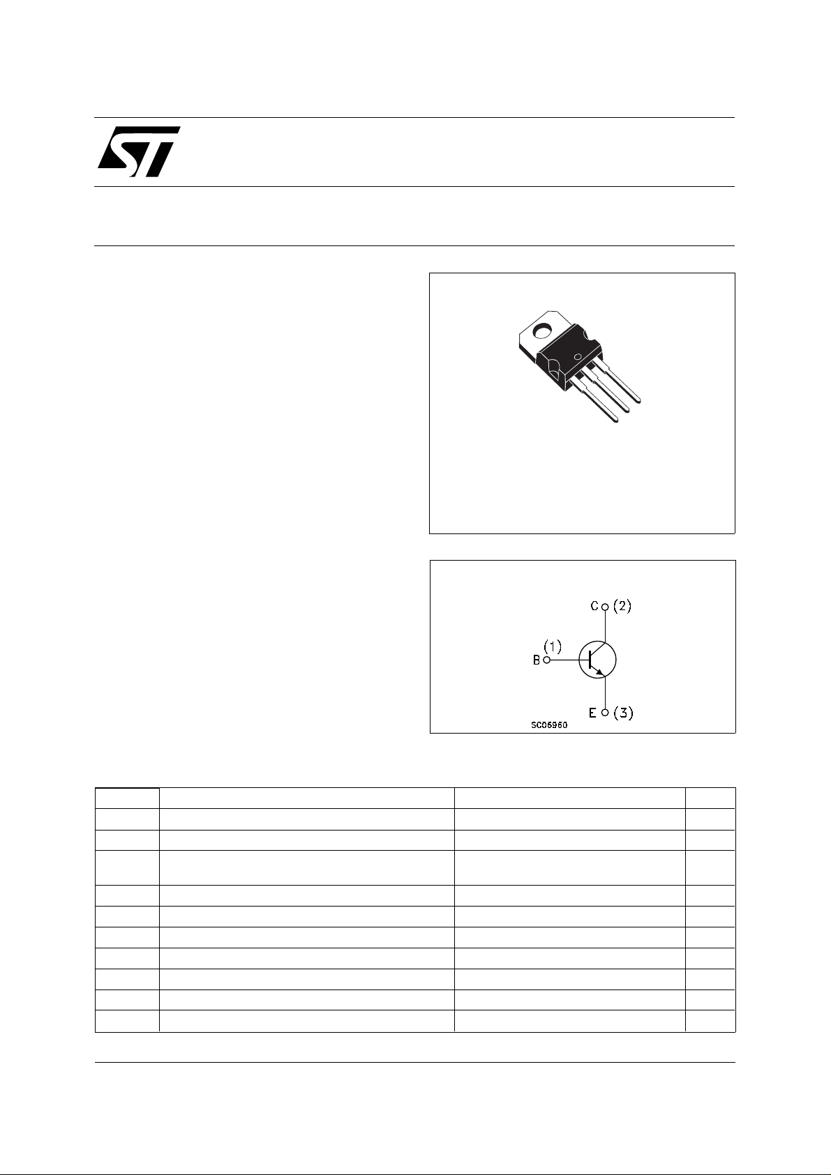
TO-220
3
2
1
The BUL742 is manufactured using high voltage
Multi Epitaxial Planar technology for high
switching speeds and high voltage capability.
It uses a Cellular Emitter structure with planar
edge termination to enhance switching speeds
while maintening the wide RBSOA.
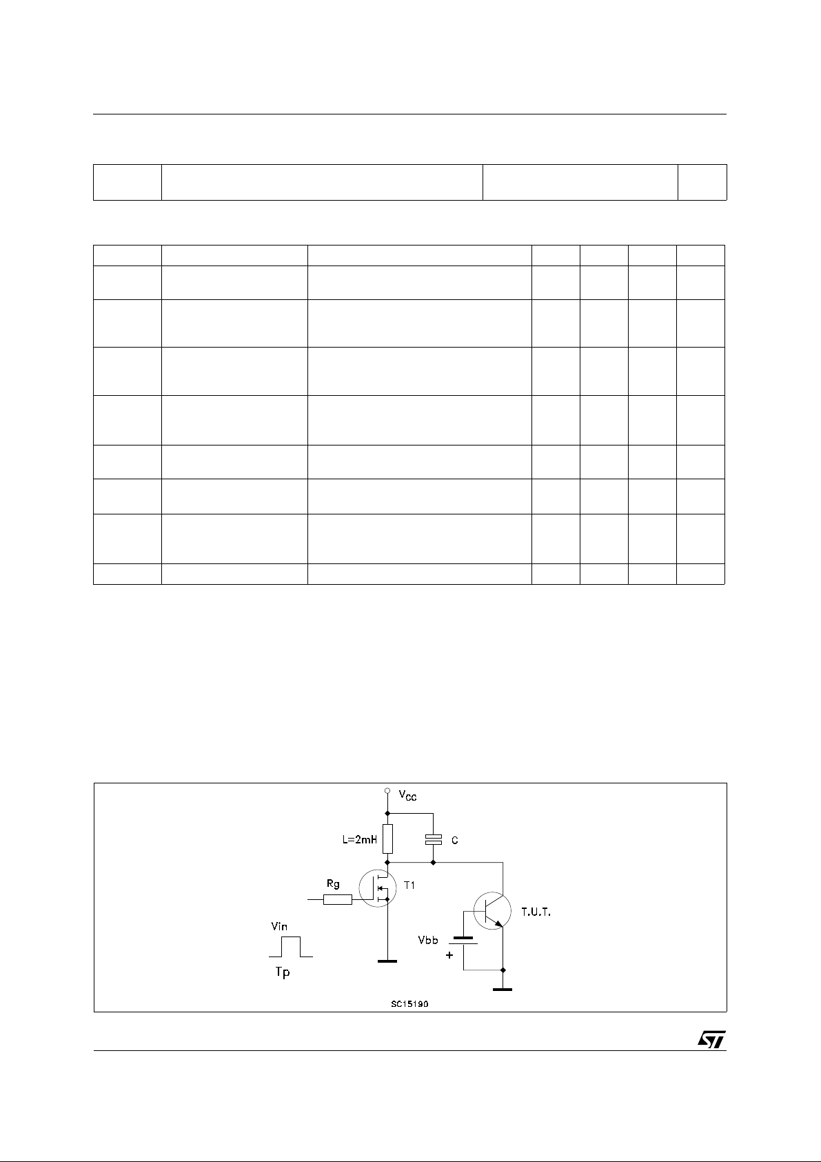
INTERNAL SCHEMAT I C DIAGRAM
Thanks to an increased intermediate layer, it has
an intrinsic ruggedness which enables the
transistor to withstand an high collector current
level during breakdown condition, without using
the transil protection usually necessary in typical
converters for lamp ballast .
ABSOLUTE MA XIMU M RAT INGS
Symbol Parameter Value Unit
V
V
V
I
I
P
T
Collector-Emitter Voltage (VBE = 0) 900 V
CES
Collector-Emitter Voltage (IB = 0) 400 V
CEO
Emitter-Base Voltage
EBO
= 0, IB = 0.75 A, tp < 10µs, Tj < 150oC)
(I
C
Collector Current 4 A
I
C
Collector Peak Current (tp <5 ms) 8 A
CM
I
Base Current 2 A
B
Base Peak Current (tp <5 ms) 4 A
BM
Total Dissipation at Tc = 25 oC70W
tot
Storage Temperature -65 to 150
stg
T
Max. Operating Junction Temperature 150
j
BV
EBO
V
o
C
o
C
June 2001
1/5
BUL742
THERMAL DATA
R
thj-case
R
thj-amb
Thermal Resistance Junction-Case Max
Thermal Resistance Junction-Ambient Max
1.78
62.5
o
C/W
o
C/W
ELECTRICAL CHARACTERISTICS (T
= 25 oC unless otherwise specif ied)
case
Symbol Parameter Test Conditions Min. Typ. Max. Unit
I
CES
V
CEO(sus)
Collector Cut-off
Current (V
BE
= 0)
∗ Collector-Emitter
= 900 V 100 µA
V
CE
= 100 mA L = 25 mH 400 V
I
C
Sustaining Voltage
(I
= 0)
B
BV
EBO
Emitter-Base
= 1 mA 12 V
I
E
Breakdown Voltage
(I
= 0)
C
V
CE(sat)
V
BE(sat)
∗ Collector-Emitter
Saturation Voltage
∗ Base-Emitter
IC = 1 A IB = 0.2 A
I
= 2 A IB = 0.4 A
C
I
= 4 A IB = 0.8 A
C
IC = 2 A IB = 0.4 A 1.5 V
0.5
1.0
1.5
Saturation Voltage
∗ DC Current Gain IC = 250 mA VCE = 5 V
h
FE
RESISTIVE LOAD
t
E
∗ Pulsed: Pulse duration = 300 µs, duty cycle 1.5 %
Storage Time
s
Fall Time
t
f
Avalanche Energy L = 2 mH 6 mJ
sb
I
= 2 A VCE = 5 V
C
V
= 125 V IC = 0.5 A
CC
I
= 45 mA IB2 = -45 mA
B1
= 300 µs
t
p
35
10
70
35
11
250
V
V
V
µs
ns
Energy Rating Test Circuit
2/5

Safe Operating A reas Derating Curve
Reverse Biased SOA
BUL742
3/5

BUL742
TO-220 MECHANICAL DATA
DIM.
A 4.40 4.60 0.173 0.181
C 1.23 1.32 0.048 0.052
D 2.40 2.72 0.094 0.107
E 0.49 0.70 0.019 0.027
F 0.61 0.88 0.024 0.034
F1 1.14 1.70 0.044 0.067
F2 1.14 1.70 0.044 0.067
G 4.95 5.15 0.194 0.202
G1 2.40 2.70 0.094 0.106
H2 10.00 10.40 0.394 0.409
L2 16.40 0.645
L4 13.00 14.00 0.511 0.551
L5 2.65 2.95 0.104 0.116
L6 15.25 15.75 0.600 0.620
L7 6.20 6.60 0.244 0.260
L9 3.50 3.93 0.137 0.154
M 2.60 0.102
DIA. 3.75 3.85 0.147 0.151
MIN. TYP. MAX. MIN. TYP. MAX.
mm inch
4/5
P011CI

BUL742
Information furnished is believed to be accurate and reliable. However, STMicroelectronics assumes no responsibility for the consequences
of use of such inform ation nor for any infringe ment o f patents or other rig hts o f third par ties which ma y resul t from i ts use. N o li cen se is
granted by implicatio n or otherwise under any patent or patent rights of STMicroelectronics. Specification mentioned in this publication are
subject to change without notice. This publication supersedes and replaces all information previously supplied. STMicroelectronics products
are not authorized for use as critical compo nents in life support devices or systems without express written approval of STMicroelectronics.
The ST logo is a trademark of STMicroelectronics
© 2001 STMicroelectro nics – Printed in Italy – All Rights Reserved
STMicroelectronics GROUP OF COMPANIES
Australia - Brazil - China - Finland - France - Germany - Hong Kong - India - Italy - Japan - Malaysia - Malta - Morocco -
Singapore - Spain - Sweden - Switzerland - United Kingdom - U.S.A.
http://www.st.com
5/5
 Loading...