

HIGH VOLTAGE FAST-SWITCHING
■ NPNTRANSISTOR
■ HIGH VOLTAGECAPABILITY
■ MINIMUMLOT-TO-LOT SPREADFOR
RELIABLEOPERATION
■ VERYHIGH SWITCHINGSPEED
■ HIGH RUGGEDNESS
APPLICATIONS
■ ELECTRONICTRANSFORMERS FOR
HALOGENLAMPS
■ SWITCHMODE POWER SUPPLIES
BUL59
NPN POWER TRANSISTOR
3
2
1
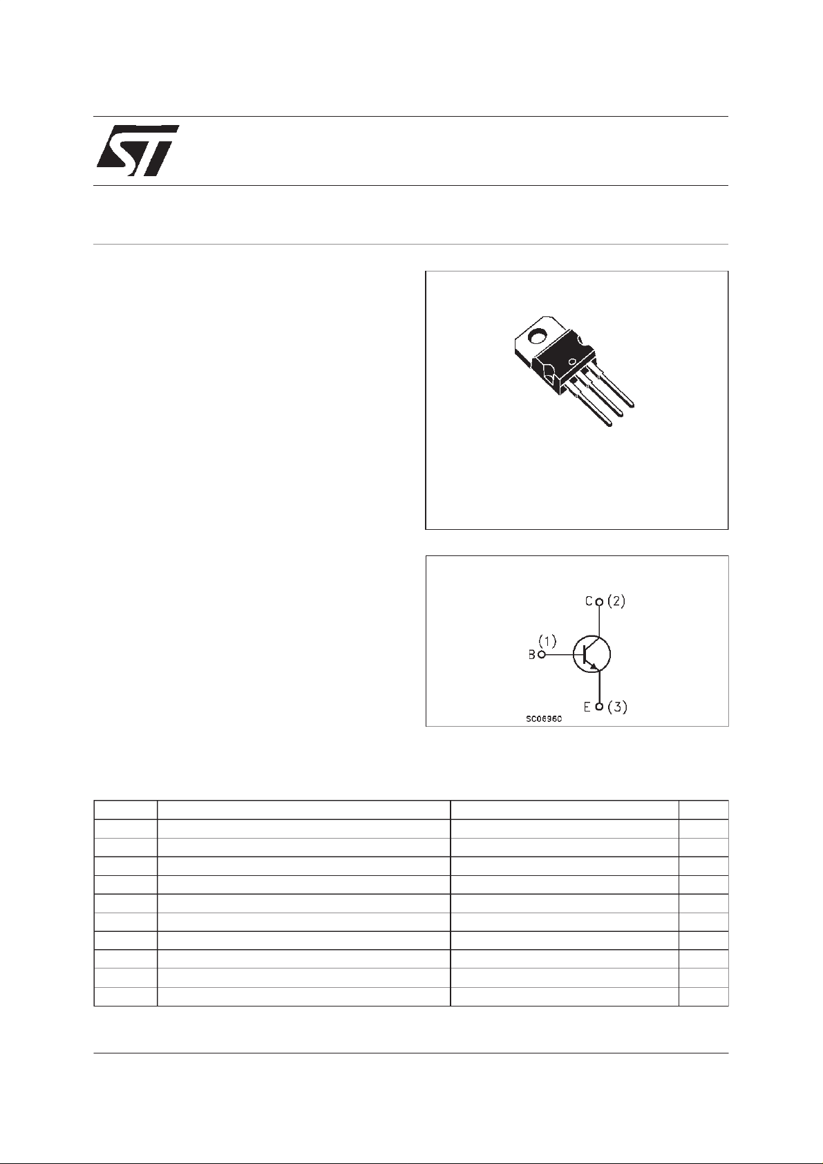
DESCRIPTION
TO-220
The BUL59 is manufactured using high voltage
Multi Epitaxial Mesa technology to enhance
switchingspeeds while maintaining wide RBSOA.
The BUL series is designed for use in lighting
applications and low cost switch-mode power
supplies.
INTERNAL SCHEMATIC DIAGRAM
ABSOLUTE MAXIMUM RATINGS
Symb o l Para meter Val u e Uni t
V
V
V
I
I
P
T
Collector-Emitter Voltage (VBE= 0) 850 V
CES
Collector-E m it ter Vo lt a ge ( I B = 0) 400 V
CEO
Emitter-Base Voltage (IC = 0) 9 V
EBO
Collector Cur rent 8 A
I
C
Collector Pe ak C urrent (tp<5 ms) 16 A
CM
Base Cu rrent 4 A
I
B
Base Pe ak Current ( tp<5 ms) 8 A
BM
Tot al Dis sipation at T c = 25oC90W
tot
Sto rage Temper ature -65 t o 150
stg
Max. O peratin g Junctio n Te mperatu re 150
T
j
o
C
o
C
June 1999
1/6
BUL59
THERMAL DATA
R
thj-case
R
thj-amb
Ther mal Resis t an c e Junct io n- C as e Max
Ther mal Resis t an c e Junct io n- Am b ient Max
1.39
62.5
o
C/W
o
C/W
ELECTRICAL CHARACTERISTICS (T
=25oC unlessotherwisespecified)
case
Symbol Parameter Test Cond itions Min. Typ. Max. Un it
I
CES
I
EBO
V
CEO(sus)
Collec t or Cut -off
Current (V
BE
=0)
Emitt er Cut -off Current
=0)
(I
C
Collec t or -Emit t er
V
=ratedV
CE
VCE=ratedV
V
=9V 100 µA
EB
I
=10mA L=25mH 400 V
C
CES
CES
Tj=125oC
200
500
Sust aining Voltage
=0)
(I
B
V
∗ Collec t or -Emit t er
CE(sat)
Saturation Voltage
V
∗ Base-Emi tter
BE(sat)
Saturation Voltage
V
CEW
Maximum Co llector
Emitt er Voltag e
Wit hout Snub ber
∗ DC C ur r ent Gain IC=2A VCE=5V
h
FE
INDUCTIVE LOAD
t
∗
Pulsed: Pulse duration = 300 µs, duty cycle 1.5 %
s
t
f
Storage Ti me
Fall Time
IC=2A IB=0.4A
I
=5A IB=1A
C
IC=2A IB=0.4A
=5A IB=1A
I
C
=15A RBB=0Ω
I
C
= - 2. 5 V L = 50 µ H
V
BB
=10µs
t
p
=5A VCE=5V
I
C
I
=8A VCE=10V
C
IC=2A I
V
V
=-5V RBB=0Ω
BE(off)
=250V L=200µH
CC
Bon
=0.4A
0.18 0.5
1.5
1.2
1.6
450 V
8
6
40
30
4
0.8
0.15
µA
µA
V
V
V
V
µs
µs
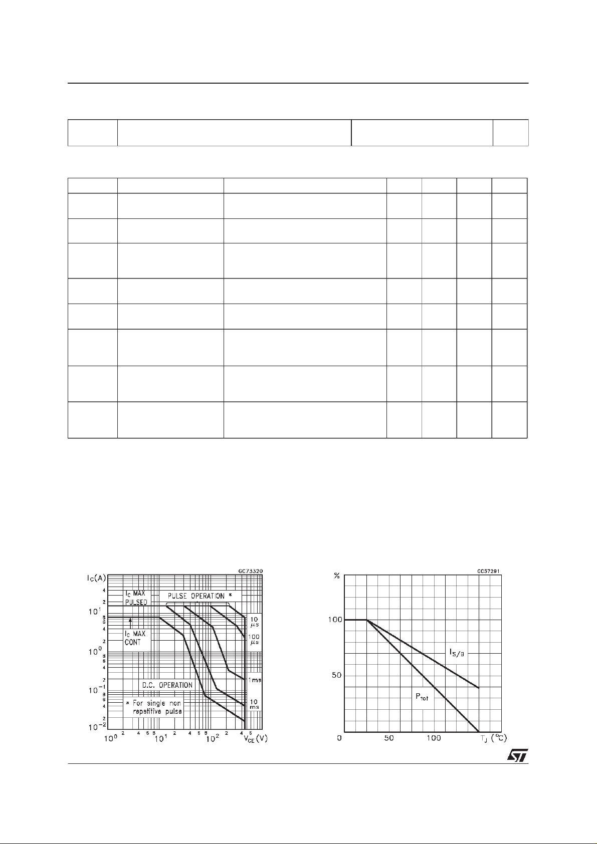
Safe Operating Areas DeratingCurve
2/6

BUL59
DCCurrent Gain
CollectorEmitterSaturationVoltage
DC Current Gain
BaseEmitterSaturationVoltage
InductiveFall Time
InductiveStorage Time
3/6

BUL59
ReverseBiasedSOA RBSOAand Inductive Load SwitchingTest
Circuit
(1) Fast electronic switch
(2) Non-inductive Resistor
(3) Fast recovery rectifier
4/6

TO-220 MECHANICAL DATA
BUL59
DIM.
MIN. TYP. MAX. MIN. TYP. MAX.
A 4.40 4.60 0.173 0.181
C 1.23 1.32 0.048 0.051
D 2.40 2.72 0.094 0.107
D1 1.27 0.050
E 0.49 0.70 0.019 0.027
F 0.61 0.88 0.024 0.034
F1 1.14 1.70 0.044 0.067
F2 1.14 1.70 0.044 0.067
G 4.95 5.15 0.194 0.203
G1 2.4 2.7 0.094 0.106
H2 10.0 10.40 0.393 0.409
L2 16.4 0.645
L4 13.0 14.0 0.511 0.551
L5 2.65 2.95 0.104 0.116
L6 15.25 15.75 0.600 0.620
L7 6.2 6.6 0.244 0.260
L9 3.5 3.93 0.137 0.154
DIA. 3.75 3.85 0.147 0.151
mm inch
P011C
5/6

BUL59
Information furnished isbelieved to beaccurate and reliable. However, STMicroelectronics assumes no responsibility for the consequences
of use of such information nor for any infringement of patents or other rights of third parties which may result from its use. No license is
granted by implication or otherwise under any patent or patent rights of STMicroelectronics. Specification mentioned in this publication are
subject to change without notice. This publication supersedes and replaces all information previously supplied. STMicroelectronics products
are not authorized for use as critical components in life support devices or systems without express written approval of STMicroelectronics.
The ST logo is a trademark of STMicroelectronics
1999 STMicroelectronics – Printed in Italy – AllRights Reserved
STMicroelectronicsGROUP OF COMPANIES
Australia - Brazil - Canada - China -France - Germany - Italy -Japan - Korea - Malaysia - Malta - Mexico - Morocco - The Netherlands-
Singapore - Spain - Sweden -Switzerland - Taiwan - Thailand - United Kingdom - U.S.A.
http://www.st.com
.
6/6
 Loading...