

HIGH VOLTAGE FAST-SWITCHING
■ NPNTRANSISTOR
■ HIGH VOLTAGECAPABILITY
■ LOW SPREADOF DYNAMIC PARAMETERS
■ MINIMUMLOT-TO-LOT SPREADFOR
RELIABLEOPERATION
■ VERYHIGH SWITCHINGSPEED
■ HIGH RUGGEDNESS
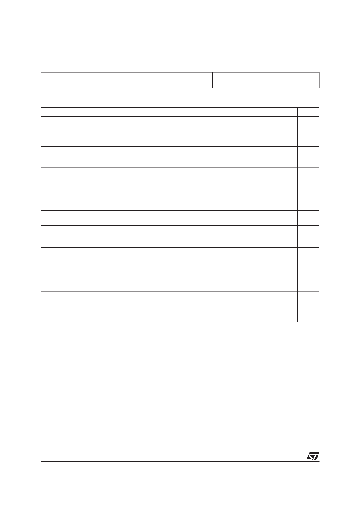
BUL49D
NPN POWER TRANSISTOR
APPLICATIONS
■ ELECTRONICTRANSFORMERS FOR
HALOGENLAMPS
■ FLYBACKANDFORWARD SINGLE
TRANSISTOR LOW POWER CONVERTERS
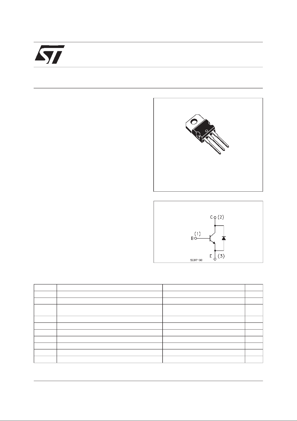
TO-220
3
2
1
DESCRIPTION
The BUL49D is manufactured using high voltage
Multi Epitaxial Planar technology for high
switchingspeeds and medium voltage capability.
The BUL49D is designed for use in electronic
INTERNAL SCHEMATIC DIAGRAM
transformersfor halogen lamps.
ABSOLUTE MAXIMUM RATINGS
Symb o l Parameter Val u e Uni t
V
V
V
I
I
P
T
Collector-Emitter Voltage ( VBE= 0) 850 V
CES
Collector-Emitter Voltage ( IB= 0) 450 V
CEO
Emitter-Base Voltage
EBO
=0, IB<2.5A, tp<10µs, TJ<150oC)
(I
C
Collect or Current 5 A
I
C
Collect or Peak Current ( tp<5ms) 10 A
CM
Base Current 2 A
I
B
Base Peak Current (tp<5ms) 4 A
BM
Tot al Di s sipation at T c = 25oC80W
tot
Storage Temperature -65 to 150
stg
Max. O perating Junct ion Tem per at u re 150
T
j
BV
EBO
V
o
C
o
C
June 2000
1/6
BUL49D
THERMAL DATA
R
thj-case
R
thj- amb
Ther mal Resistance Junct ion-Case Max
Thermal Resistance Junction-Ambient Max
1.56
62.5
o
C/W
o
C/W
ELECTRICAL CHARACTERISTICS (T
=25oC unlessotherwisespecified)
case
Symbol Parameter Test C ondition s Min. Typ. Max. Unit
BV
I
I
CES
EBO
EBO
Collector C ut -off
Current (V
BE
=0)
Emit ter Cut -o f f C urr ent
(I
=0)
C
Emitt er-Base
V
=850V
CE
=850V Tj=125oC
V
CE
=9V 100 µA
V
EB
I
=10mA 10 18 V
E
100
500
Break dow n Volt age
=0)
(I
C
V
CEO(sus)
∗ Co llec tor-Emitt er
I
=10mA L=25mH 450 V
C
Sust aining Volt age
=0)
(I
B
V
∗ Collector-E mitter
CE(sat)
Saturation Voltage
V
∗ Base-Emitt er
BE(sat )
Saturation Voltage
h
∗ DC C urr ent Gain IC=10mA VCE=5V
FE
V
CEW
Maximum Collector
Emit ter Voltage
Wit hout Snubber
RESI STIVE LO AD
s
t
f
St orage Time
Fall T ime
t
INDUCTIVE LO A D
t
V
∗
Pulsed: Pulse duration = 300 µs, duty cycle 1.5 %
St orage Time
s
t
Fall T ime
f
Diode Forward Voltage IC=3A 1.5 V
f
IC=1A IB=0.2A
=2A IB=0.4A
I
C
=4A IB=0.8A
I
C
IC=1A IB=0.2A
=4A IB=0.8A
I
C
=0.5A VCE=5V
I
C
=7A VCE=10V
I
C
=8A RBB=0Ω
I
C
=-2.5V L=50µH
V
BB
=10µs
t
p
IC=2A VCC= 250 V
I
B(on)=IB(off)
IC=4A I
V
V
=-5V RBB=0Ω
BE(of f )
= 300 V L = 1 mH
CL
10
4
450 V
=0.4A 2 3
=0.8A
B(on)
0.1 0.3
0.6
1.2
1.0
1.3
60
10
0.8
0.6
50
1.3
100
µA
µA
V
V
V
V
V
µs
µs
µs
ns
2/6

BUL49D
Safe Operating Areas
DCCurrent Gain
DeratingCurve
DC Current Gain
CollectorEmitterSaturationVoltage
BaseEmitterSaturationVoltage
3/6

BUL49D
InductiveFall Time
ReverseBiasedSOA
InductiveStorageTime
4/6

TO-220 MECHANICAL DATA
BUL49D
DIM.
MIN. TYP. MAX. MIN. TYP. MAX.
A 4.40 4.60 0.173 0.181
C 1.23 1.32 0.048 0.051
D 2.40 2.72 0.094 0.107
D1 1.27 0.050
E 0.49 0.70 0.019 0.027
F 0.61 0.88 0.024 0.034
F1 1.14 1.70 0.044 0.067
F2 1.14 1.70 0.044 0.067
G 4.95 5.15 0.194 0.203
G1 2.4 2.7 0.094 0.106
H2 10.0 10.40 0.393 0.409
L2 16.4 0.645
L4 13.0 14.0 0.511 0.551
L5 2.65 2.95 0.104 0.116
L6 15.25 15.75 0.600 0.620
L7 6.2 6.6 0.244 0.260
L9 3.5 3.93 0.137 0.154
DIA. 3.75 3.85 0.147 0.151
mm inch
P011C
5/6

BUL49D
Information furnished isbelieved to beaccurate and reliable. However, STMicroelectronics assumes no responsibility for the consequences
of use of such information nor for any infringement of patents or other rights of third parties which may result from its use. No license is
granted by implication or otherwise under any patent or patent rights of STMicroelectronics. Specification mentioned in thispublication are
subject to change without notice. This publication supersedes and replaces all information previously supplied. STMicroelectronics products
are not authorized for use as critical components in life support devices or systems without express written approval of STMicroelectronics.
The ST logo is a trademark of STMicroelectronics
2000 STMicroelectronics – Printedin Italy – All Rights Reserved
STMicroelectronicsGROUP OF COMPANIES
Australia - Brazil - China - Finland- France- Germany- HongKong - India- Italy- Japan -Malaysia - Malta -Morocco -
Singapore-Spain - Sweden - Switzerland -United Kingdom - U.S.A.
http://www.st.com
6/6
 Loading...