SGS Thomson Microelectronics BUL38D Datasheet

HIGH VOLTAGE FAST-SWITCHING
■ STMicroelectronics PREFERRED
SALESTYPE
■ HIGH VOLTAGECAPABILITY
■ LOW SPREAD OF DYNAMICPARAMETERS
■ MINIMUMLOT-TO-LOT SPREAD FOR
RELIABLEOPERATION
■ LOW BASE-DRIVEREQUIREMENTS
■ VERYHIGH SWITCHINGSPEED
■ FULLYCHARACTERISED AT 125
■ HIGH RUGGEDNESS
■ INTEGRATED ANTIPARALLEL
COLLECTOR-EMITTERDIODE
APPLICATIONS
■ ELECTRONICTRANSFORMERS FOR
HALOGENLAMPS
■ SWITCHMODEPOWER SUPPLIES
o
C
BUL38D
NPN POWER TRANSISTOR
3
2
1
TO-220
DESCRIPTION
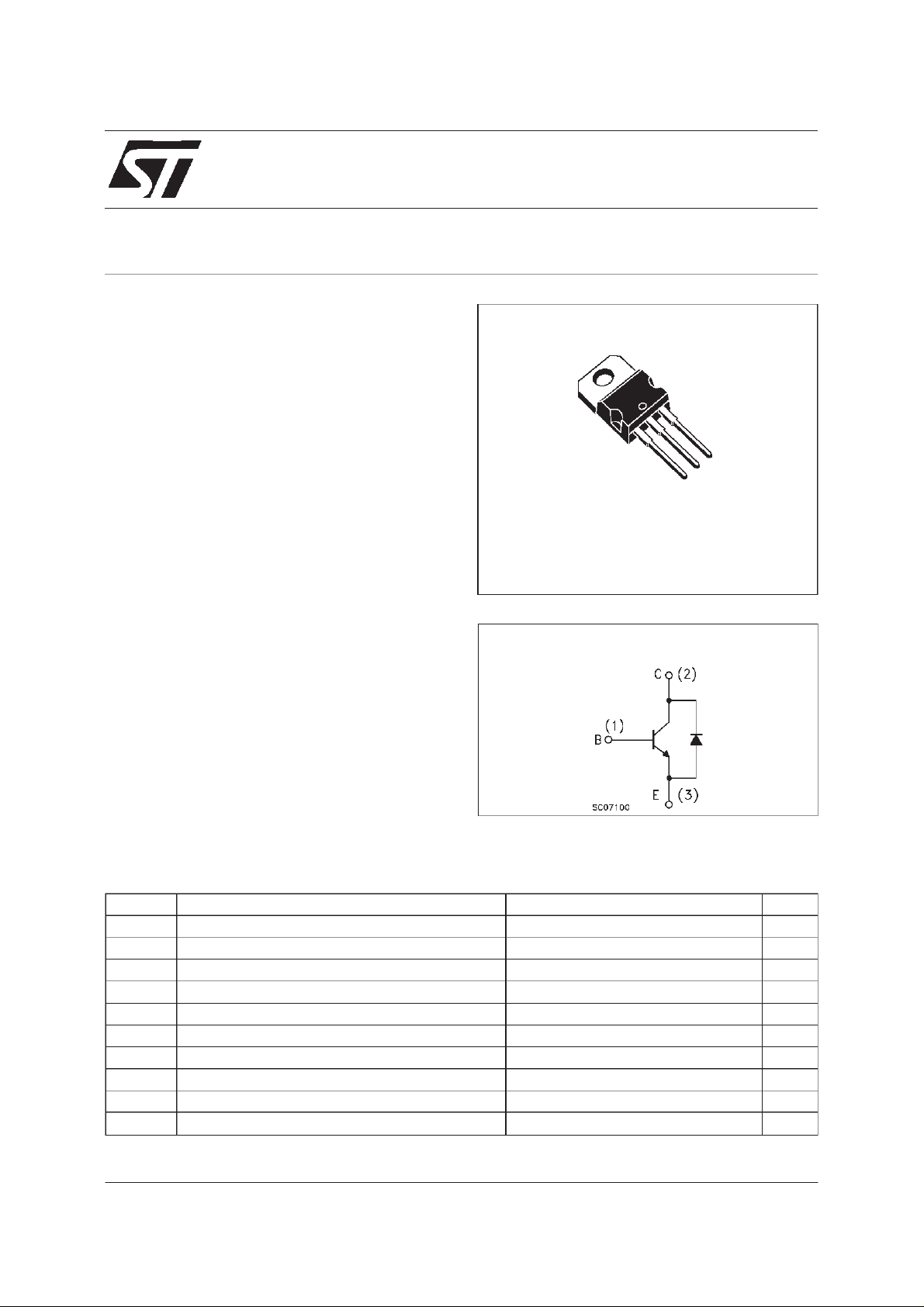
INTERNAL SCHEMATIC DIAGRAM
The BUL38D is manufacturedusing high voltage
Multi Epitaxial Planar technology for high
switching speeds and high voltage withstand
capability.
The BUL series is designed for use in lighting
applications and low cost switch-mode power
supplies.
ABSOLUTE MAXIMUM RATINGS
Symb o l Para meter Val u e Uni t
V
V
V
I
I
P
T
Collector-Emitter Voltage (VBE= 0 ) 800 V
CES
Collector-Emitter Voltage (IB= 0 ) 450 V
CEO
Emitter-Base Voltage (IC=0) 9 V
EBO
I
Collector Current 5 V
C
Collector Peak Current (tp<5 ms) 1 0 A
CM
I
Base Current 2 A
B
Base Peak Curre nt (tp<5 ms) 4 A
BM
Tot al Diss ip at i on at Tc = 25oC80W
tot
Sto rage T emperat ure -65 to 150
stg
Max. Oper at in g Junct ion Te mperatu re 150
T
j
o
C
o
C
June 2000
1/6

BUL38D
THERMAL DATA
R
thj-case
R
thj-amb
Ther mal Resistan ce Junct ion-Case Max
Ther mal Resistan ce Junct ion-Am bie nt Max
1.56
62.5
o
C/W
o
C/W
ELECTRICAL CHARACTERISTICS (T
=25oC unlessotherwise specified)
case
Symbol Parameter Test Cond ition s Min. Typ. Max. Un it
I
CES
I
CEO
V
CEO(sus)
Collec t or Cut -off
Current (V
BE
=0)
Collec t or Cut -off
Current (I
B
=0)
∗ Collec tor -Emit t er
V
=800V
CE
=800V Tj=125oC
V
CE
V
= 450 V 250 µA
CE
I
= 10 0 mA L = 25 mH 450 V
C
100
500
Sust aining Voltage
=0)
(I
B
V
EBO
V
CE(sat)
V
BE(sat)
h
FE
t
t
t
V
∗
Pulsed: Pulse duration = 300 µs, duty cycle1.5 %.
The product is pre-selected in DC current gain (Group A and Group B). STMicroelectronics reserves the right to ship either groups
according to production availability. Please contact your nearest STMicrolectronics salesoffice for deliverydatails.
Emitter-Base Voltage
(I
=0)
C
∗ Collector-Emit t er
Saturation Voltage
∗ Base-Emitt er
Saturation Voltage
∗ DC Current Ga in IC=10mA VCE=5V
RESI STIVE LOAD
Storage Time
s
t
Fall Time
f
INDUCTIVE LO AD
Storage Time
s
t
Fall Time
f
INDUCTIVE LO AD
Storage Time
s
t
Fall Time
f
Diode Forward V oltage IC=2A 1.5 V
f
=10mA 9 V
I
E
IC=1A IB=0.2A
=2A IB=0.4A
I
C
=3A IB=0.75A
I
C
IC=1A IB=0.2A
=2A IB=0.4A
I
C
10
=0.5A VCE=5V
I
C
=2A VCE=5V
I
C
Gr oup A
Gr oup B
13
22
IC=2.5A VCC=150V
=-IB2=0.5A tp=30µs
I
B1
1.0 2.2
IC=2A IB1=0.4A
V
V
=-5V RBB=0Ω
BE(off)
= 2 50 V L = 200 µH
CL
1
55
IC=2A IB1=0.4A
V
V
T
=-5V RBB=0Ω
BE(off)
= 2 50 V L = 200 µH
CL
=125oC
j
1.3
100
0.5
0.7
1.1
1.1
1.2
60
23
32
0.8
1.8
100
µA
µA
V
V
V
V
V
µs
µs
µs
ns
µs
ns
2/6
 Loading...