

HIGH VOLTAGE FAST-SWITCHING
Ordering Code Marking Shipment
BUL312FH BUL312FH Tube
HIGH VOLTAGE CAPABILITY
LOW SPREAD OF DYNAMIC PARAM ETE R S
MINIMUM LOT-TO-LOT SPREAD FOR
RELIABLE OPERATION
VERY HIGH SWITCHING SPEED
FULLY CHARACTERIZED AT 125 °C
LARGE R.B.S.O.A.
FULLY INSULATED PAC KAG E ( U .L .
COMPLIANT) FOR EASY MOUNTING
APPLICATIONS:
HORIZONTAL DEFLECTION FOR COLOR TV
SWITCH MODE POWER SUPPLI ES
ELECTRONIC BALLASTS FOR
FLUORE S C ENT LIGHTIN G
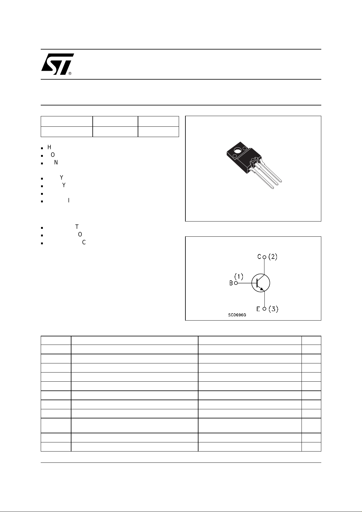
BUL312FH
NPN POWER TRANSISTOR
TO-220FH
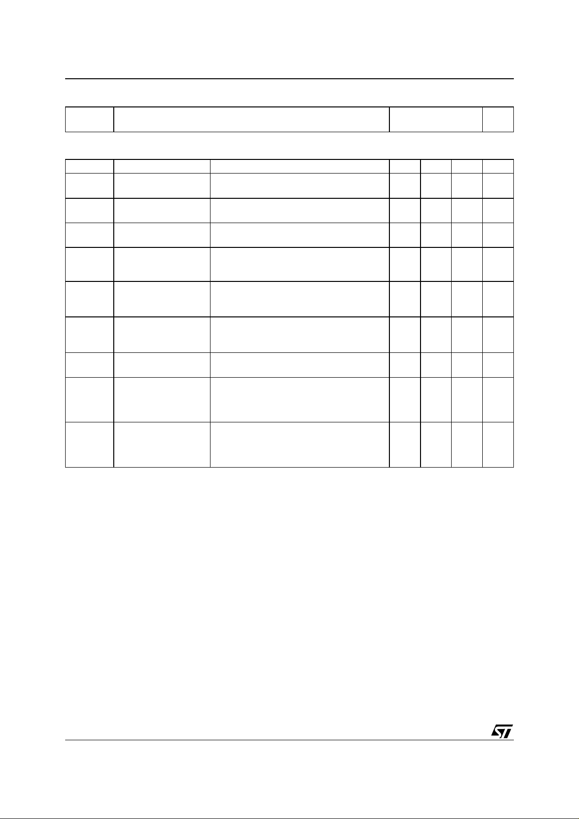
INTERNAL SCHEMATIC DIAGRAM
DESC RI PTIO N
The device is manufactured us ing High Voltage
Multi Epitaxial Planar technology for h igh switching
speeds and high voltage capability.
It uses a Cellular Emitter structure with planar edge
termination to enhance switching speeds while
maintaining a wide R.B.S.O.A.
ABSOLUTE MAXIMUM RATINGS
Symbol Parameter Value Unit
V
CES
V
CEO
V
EBO
I
I
CM
I
I
BM
P
V
isol
T
stg
T
Collector-Emitter Voltage (VBE = 0)
Collector-Emitter Voltage (IB = 0)
Emitter-Base Voltage (IC = 0)
Collector Current 5 A
C
Collector Peak Current (tp < 5 ms)
Base Current 3 A
B
Base Peak Current (tp < 5 ms)
Total Dissipation at Tc = 25 °C
tot
Insulation Withstand Voltage (RMS) from All Three
Leads to External Heatsink
Storage Temperature –65 to 150 °C
Max. Operating Junction Temperature 150 °C
j
1150 V
500 V
9V
10 A
4A
36 W
2500 V
1/6August 2002
BUL312FH
THERMA L D ATA
R
thj-case
R
thj-amb
Thermal Resistance Junction-c ase
Thermal Resistance Junction-a mbie nt
Max
Max
3.47
62.5
°C/W
°C/W
ELECTRICAL CHARACTERISTICS (T
= 25 °C unless otherwise specified)
j
Symbol Parameter Test Conditions Min. Typ. Max. Unit
I
CES
I
CEO
V
EBO
V
CEO(sus)
Collector Cut-off
Current (V
BE
= 0)
Collector Cut-off
Current (I
= 0)
B
Emitter-Base Voltage
= 0)
(I
C
* Collector-Emitter
= 1150 V
V
CE
V
= 1150 V
CE
V
= 500 V 250 µA
CE
I
= 10 mA 9 V
E
I
= 100 mA 500 V
C
= 125 °C
T
j
1
2
Sustaining Voltage
= 0)
(I
B
V
* Collector-Emitter
CE(sat)
Saturation Voltage
* Base-Emitter
V
BE(sat)
Saturation Voltage
* DC Current Gain IC = 10 mA
h
FE
INDUCTIVE LOAD
t
t
Storage Time
s
Fall Time
f
IC = 1 A
I
= 2 A
C
I
= 3 A
C
IC = 1 A
I
= 2 A
C
I
= 3 A
C
I
= 3 A
C
IC = 2 A
I
= 400 mA
B1
L = 200 µH
= 200 mA
I
B
I
= 400 mA
B
I
= 600 mA
B
= 200 mA
I
B
I
= 400 mA
B
I
= 600 mA
B
= 5 V
V
CE
V
= 2.5 V
CE
= 250 V
V
clamp
V
BE(off)
R
= 0
BB
= -5 V
0.5
0.7
1.1
1
1.1
1.2
8
816
1.2
80
1.9
160µsns
(See Figure 1)
INDUCTIVE LOAD
s
f
Storage Time
Fall Time
t
t
* Pulsed: Pu lse duration = 300 µs, dut y c ycle = 1.5 %.
IC = 2 A
I
= 400 mA
B1
L = 200 µH
T
= 125 °C
j
= 250 V
V
clamp
V
= -5 V
BE(off)
R
= 0
BB
(See Figure 1)
1.8
150
mA
mA
V
V
V
V
V
V
µs
ns
2/6

Safe Operating Area Derating Curve
Base-Emitter Saturation VoltageCollector-Emitter Saturation Voltage
BUL312FH
DC Current GainDC Current Gain
3/6

BUL312FH
Inductive Load Storage Time
Reverse Biased Safe Operating Area
Inductive Load Fall Time
Figure 1: Inductive Load Switching T est Circuit
1) Fast Electronic Switch
2) Non-Inductive Resistor
3) Fast Recovery Rectifier
4/6

TO-220FH (Fully plastic High voltage) MECHANICAL DATA
BUL312FH
DIM.
A 4.4 4.6 0.173 0.181
B 2.5 2.7 0.098 0.106
D 2.5 2.75 0.098 0.108
E 0.45 0.7 0.017 0.027
F 0.75 1 0.030 0.039
F1 1.3 1.8 0.051 0.070
F2 1.3 1.8 0.051 0.070
G 4.95 5.2 0.195 0.204
G1 2.4 2.7 0.094 0.106
H 10 10.4 0.393 0.409
L2 16 0.630
L3 28.6 30.6 1.126 1.204
L4 9.8 10.6 0.385 0.417
L5 3.4 0.134
L6 15.9 16.4 0.626 0.645
L7 9 9.3 0.354 0.366
L8 14.5 15 0.570 0.590
L9 2.4 0.094
MIN. TYP. MAX. MIN. TYP. MAX.
mm inch
P011W
5/6

BUL312FH
Information furnished is believed to be accurate and reliable. However, STMicroelectronics assumes no responsibility f or t he
consequences of use of su ch in formation nor for any infri ngement of p atents or other rights of third parties w hich may result from
its use. No license is granted by implication or otherwise under any patent or patent rights of STMicroelectronics. Specifications
mentioned in this publication are subject to change without notice. This publication supersedes and replaces all information
previously suppli ed. STMi croelect ronics products are not author ized for use as c ritical component s in li fe suppo rt dev ices or
systems without express written approval of STMicroelectronics.
Australia - Brazil - Canada - China - Finland - France - Germany - Hong Kong - India - Israel - Italy - Japan - Malaysia - Malta - Morocco
© The ST logo is a registered trademark of STMicroelectronics
© 2002 STMicroelectronics - Printed in Italy - All Rights Reserved
Singapore - Spain - Sweden - Switzerland - United Kingdom - United States.
STMicroelectronics GROUP OF COMPANIES
© http://www.st.com
6/6
 Loading...