


HIGH VOLTAGE FAST-SWITCHING
■ SGS-THOMSONPREFERRED SALESTYPES
■ NPNTRANSISTOR
■ HIGH VOLTAGECAPABILITY
■ LOW SPREADOF DYNAMICPARAMETERS
■ MINIMUMLOT-TO-LOT SPREADFOR
RELIABLEOPERATION
■ VERYHIGH SWITCHINGSPEED
■ FULLYCHARACTERISEDAT 125
■ LARGERBSOA
■ U.L.RECOGNISED ISOWATT220PACKAGE
(U.L. FILE # E81734(N)):
ISOLATIONVOLTAGE1500V
APPLICATIONS
■ ELECTRONICBALLASTSFOR
FLUORESCENT LIGHTING
■ FLYBACKAND FORWARD SINGLE
TRANSISTOR LOW POWER CONVERTERS
DESCRIPTION
The BUL310 and BUL310PI are manufactured
using high voltage Multi Epitaxial Planar
technology for high switching speeds and high
voltage capability. They use a Cellular Emitter
structurewith planar edge terminationto enhance
switching speeds while maintaining a wide
RBSOA.
The BUL series is designed for use in lighting
applications and low cost switch-mode power
supplies.
RMS
o
C
BUL310
BUL310PI
NPN POWER TRANSISTORS
3
2
1
TO-220 ISOWATT220
INTERNAL SCHEMATIC DIAGRAM
3
2
1
ABSOLUTE MAXIMUM RATINGS
Symb o l Parameter Val u e Uni t
BUL310 BUL310PI
V
V
V
I
I
P
T
September 1997
Collector-Emitter Voltage ( VBE= 0) 1000 V
CES
Collector-Emitter Voltage ( IB= 0) 500 V
CEO
Emitter-Base Voltage ( IC=0) 9 V
EBO
Collect or Current 5 V
I
C
Collect or Peak Current (tp<5 ms) 10 A
CM
Base Current 3 A
I
B
Base Peak Curr ent (tp<5 ms) 4 A
BM
Tot al Dissipation at T c = 25oC7535W
tot
Storage Temperature -65 to 1 50
stg
Max. O per ating Junct ion T emperature 150
T
j
o
C
o
C
1/7

BUL310/PI
THERMAL DATA
R
thj-case
R
thj-amb
Ther mal Resistance Ju nc t io n-Cas e Max
Thermal Resistance Junction-Ambient Max
TO - 220 IS O WATT220
1.65
62.5
3.58
62.5
o
C/W
o
C/W
ELECTRICAL CHARACTERISTICS (T
=25oC unless otherwise specified)
case
Symbol Parameter Test Cond ition s Min. Typ. Max. Unit
I
CES
I
CEO
V
CEO(sus)
Collector C ut -off
Current (V
BE
=0)
Collector C ut -off
Current (I
B
=0)
Collector-Emit t er
V
=1000V
CE
=1000V Tj= 125oC
V
CE
=400V 250 µA
V
EC
100
500
IC= 100 mA L= 25 mH 500 V
Sust aining V olt ag e
V
V
CE(sat)
EBO
Emitt er-Base V oltage
=0)
(I
C
∗ Co llector-Em itt er
Saturation Voltage
V
∗ Base-Emitt er
BE(sat)
Saturation Voltage
h
∗ DC C urr ent Gain IC=10mA VCE=5V
FE
INDUCTIVE LOAD
t
s
t
f
St orage Time
Fall T ime
INDUCTIVE LOAD
t
∗
Pulsed: Pulse duration = 300 µs, duty cycle 1.5 %
s
t
f
St orage Time
Fall T ime
I
=10mA 9 V
E
IC=1A IB=0.2A
=2A IB=0.4A
I
C
I
=3A IB=0.6A
C
IC=1A IB=0.2A
=2A IB=0.4A
I
C
=3A IB=0.6A
I
C
0.5
0.7
1.1
1
1.1
1.2
10
I
=3A VCE=2.5V
C
10
IC=2A IB1=0.4A
V
V
=-5V RBB=0Ω
BE(off)
= 250 V L = 200 µ H
CL
1.2
80
1.9
160
IC=2A IB1=0.4A
V
V
T
=-5V RBB=0Ω
BE(off)
= 250 V L = 2 00 µ H
CL
= 125oC
j
1.8
150
µA
µA
V
V
V
V
V
V
µs
ns
µs
ns
Safe Operating Areas DeratingCurve
2/7

BUL310/PI
DCCurrent Gain
CollectorEmitter SaturationVoltage
DC Current Gain
BaseEmitter Saturation Voltage
InductiveFall Time
InductiveStorage Time
3/7

BUL310/PI
ReverseBiased SOA RBSOAand InductiveLoad SwitchingTest
Circuit
(1) Fast electronic switch
(2) Non-inductive Resistor
(3) Fast recovery rectifier
4/7

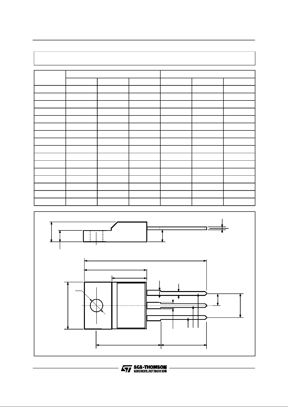
TO-220 MECHANICALDATA
BUL310/PI
DIM.
MIN. TYP. MAX. MIN. TYP. MAX.
A 4.40 4.60 0.173 0.181
C 1.23 1.32 0.048 0.051
D 2.40 2.72 0.094 0.107
D1 1.27 0.050
E 0.49 0.70 0.019 0.027
F 0.61 0.88 0.024 0.034
F1 1.14 1.70 0.044 0.067
F2 1.14 1.70 0.044 0.067
G 4.95 5.15 0.194 0.203
G1 2.4 2.7 0.094 0.106
H2 10.0 10.40 0.393 0.409
L2 16.4 0.645
L4 13.0 14.0 0.511 0.551
L5 2.65 2.95 0.104 0.116
L6 15.25 15.75 0.600 0.620
L7 6.2 6.6 0.244 0.260
L9 3.5 3.93 0.137 0.154
DIA. 3.75 3.85 0.147 0.151
mm inch
P011C
5/7
BUL310/PI
ISOWATT220MECHANICAL DATA
DIM.
MIN. TYP. MAX. MIN. TYP. MAX.
A 4.4 4.6 0.173 0.181
B 2.5 2.7 0.098 0.106
D 2.5 2.75 0.098 0.108
E 0.4 0.7 0.015 0.027
F 0.75 1 0.030 0.039
F1 1.15 1.7 0.045 0.067
F2 1.15 1.7 0.045 0.067
G 4.95 5.2 0.195 0.204
G1 2.4 2.7 0.094 0.106
H 10 10.4 0.393 0.409
L2 16 0.630
L3 28.6 30.6 1.126 1.204
L4 9.8 10.6 0.385 0.417
L6 15.9 16.4 0.626 0.645
L7 9 9.3 0.354 0.366
Ø 3 3.2 0.118 0.126
mm inch
E
A
D
B
L3
L6
L7
¯
F1
F
G1
H
G
F2
123
L2
L4
P011G
6/7

BUL310/PI
Informationfurnished is believed to be accurate and reliable.However, SGS-THOMSON Microelectronics assumes no responsability for the
consequencesof use of such information nor for any infringementof patents or other rights of third parties which may results fromits use.No
license is granted byimplicationor otherwiseunder anypatentor patentrights ofSGS-THOMSONMicroelectronics.Specificationsmentioned
in thispublication are subject to change without notice. This publicationsupersedesand replaces all informationpreviously supplied.
SGS-THOMSON Microelectronicsproducts are notauthorizedfor use ascritical componentsin lifesupportdevices or systemswithout express
written approvalof SGS-THOMSONMicroelectonics.
1997 SGS-THOMSON Microelectronics - Printed in Italy - All Rights Reserved
Australia- Brazil - Canada- China- France- Germany- Hong Kong - Italy - Japan- Korea -Malaysia - Malta - Morocco - The Netherlands -
Singapore - Spain - Sweden - Switzerland - Taiwan - Thailand - United Kingdom- U.S.A
SGS-THOMSON MicroelectronicsGROUP OF COMPANIES
...
7/7
 Loading...