

SGS Thomson Microelectronics BUL128FP Datasheet
HIGH VOLTAGE FAST-SWITCHING
■ SGS-THOMSONPREFERRED SALESTYPE
■ NPNTRANSISTOR
■ HIGH VOLTAGECAPABILITY
■ LOW SPREADOF DYNAMICPARAMETERS
■ MINIMUMLOT-TO-LOT SPREADFOR
RELIABLEOPERATION
■ VERYHIGH SWITCHINGSPEED
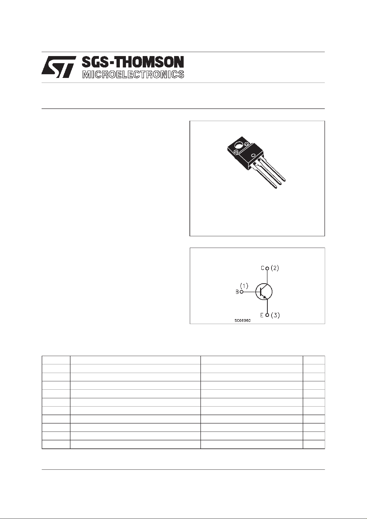
BUL128FP
NPN POWER TRANSISTOR
APPLICATIONS:
■ ELECTRONICBALLASTSFOR
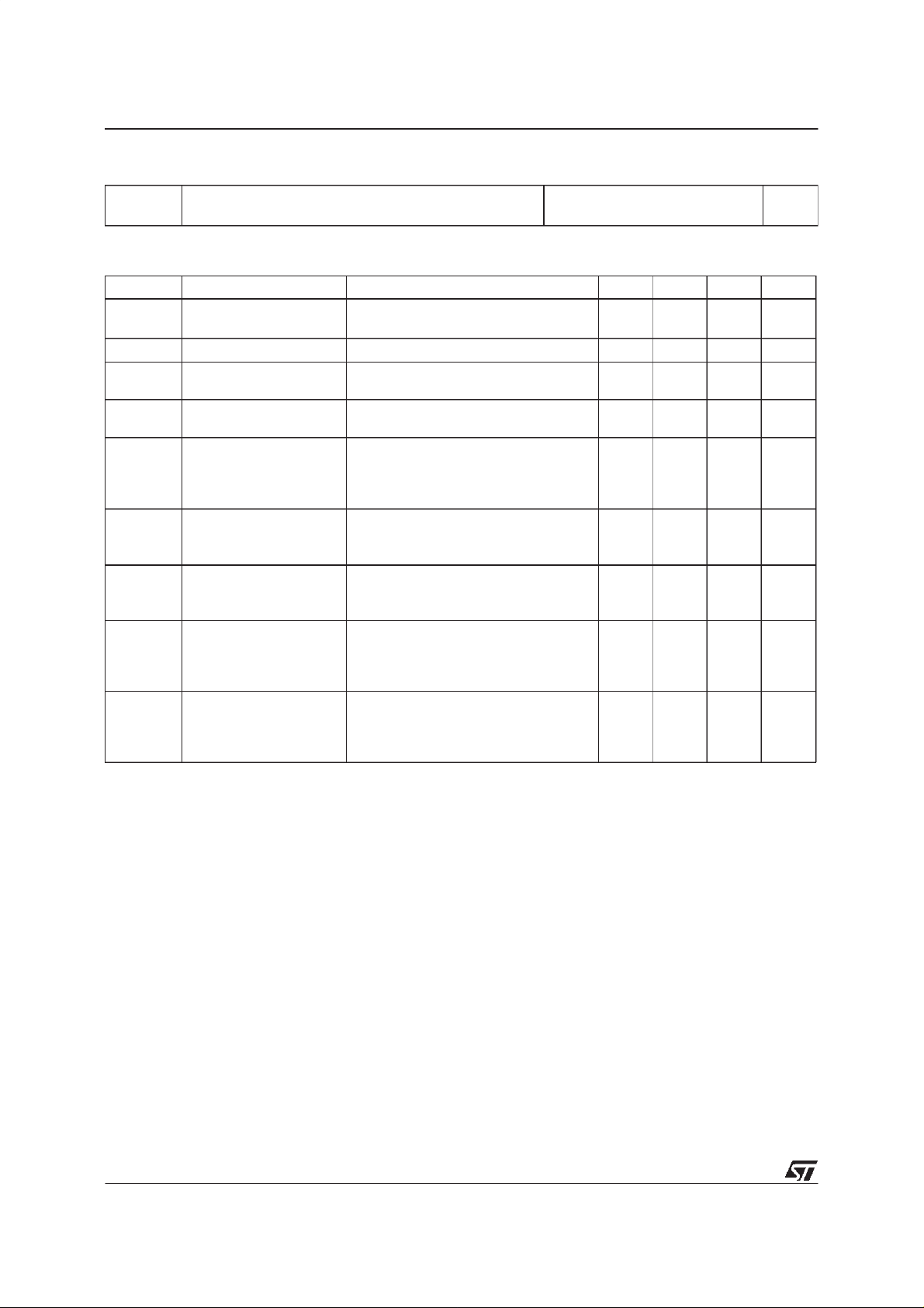
3
2
1
FLUORESCENT LIGHTING
DESCRIPTION
TO-220FP
The device is manufactured using high voltage
Multi Epitaxial Planar technology for high
switchingspeeds and medium voltage capability.
It uses a Cellular Emitter structure with planar
edge termination to enhance switching speeds
while maintainingthe wide RBSOA.
INTERNAL SCHEMATIC DIAGRAM
The device is designed for use in lighting
applications and low cost switch-mode power
supplies.
ABSOLUTE MAXIMUM RATINGS
Symb o l Parame t er Val u e Uni t
V
V
V
I
I
P
T
Collector-Emitter Voltage (VBE= 0) 700 V
CES
Collector-Emitter Voltage (IB= 0) 400 V
CEO
Emitter-Base Voltage (IC=0) 9 V
EBO
Collect or Current 4 A
I
C
Collect or Peak Current ( tp<5ms) 8 A
CM
Base Current 2 A
I
B
Base Peak Current (tp<5ms) 4 A
BM
Total Dissipat ion at Tc=25oC31W
tot
Stora ge T emperature -65 to 150
stg
Max. Oper at i ng Junct i on T emperat u re 150
T
j
o
C
o
C
April 1998
1/7
BUL128FP
THERMAL DATA
R
thj-case
R
thj- amb
Ther mal Resistance Junc tion-Case Max
Thermal Resistance Junction-Ambient Max
4.1
62.5
o
C/W
o
C/W
ELECTRICAL CHARACTERISTICS (T
=25oC unlessotherwise specified)
case
Symbol Parameter Test Cond ition s Min. Typ. Max. Unit
I
CES
V
EBO
V
CEO(sus)
Collector C ut -off
Current (V
=-1.5V)
BE
=700V
V
CE
V
=700V Tj=125oC
CE
100
500
Emitt er-Base V oltage IE=10mA 9 V
Collector-E mitt er
IC= 100 mA L = 25 mH 400 V
Sust aining Volt age
I
V
CE(sat)
CEO
Collector C ut -Of f
Current (I
B
=0)
∗ Collector- Emitt er
Saturation Voltage
V
∗ Base-Emitt er
BE(sat )
Saturation Voltage
h
∗ DC C urr ent Gain IC=10mA VCE=5V
FE
RESI STIVE LO AD
t
s
t
f
St orage Time
Fall T ime
V
=400V 250 µA
CE
IC=0.5A IB=0.1A
=1A IB=0.2A
I
C
=2.5A IB=0.5A
I
C
=4A IB=1A 0.5
I
C
IC=0.5A IB=0.1A
I
=1A IB=0.2A
C
=2.5A IB=0.5A
I
C
0.7
1
1.5
1.1
1.2
1.3
10
=1A VCE=5V
I
C
=2A VCE=5V
I
C
15
14
45
40
VCC=125 V IC=2A
=0.4A IB2=-0.4A
I
B1
=30µs
T
p
1.9
0.2
2.9
0.4
(see f ig. 2)
INDUCTI V E LOA D
t
s
t
f
St orage Time
Fall T ime
IC=2A IB1=0.4A
=-5V RBB=0Ω
V
BEo f f
V
clamp
= 200 V
0.6
0.1
1
0.2
(see f ig. 1)
∗
Pulsed: Pulse duration = 300 µs, duty cycle 1.5 %
µA
µA
V
V
V
V
V
V
V
µs
µs
µs
µs
2/7
BUL128FP
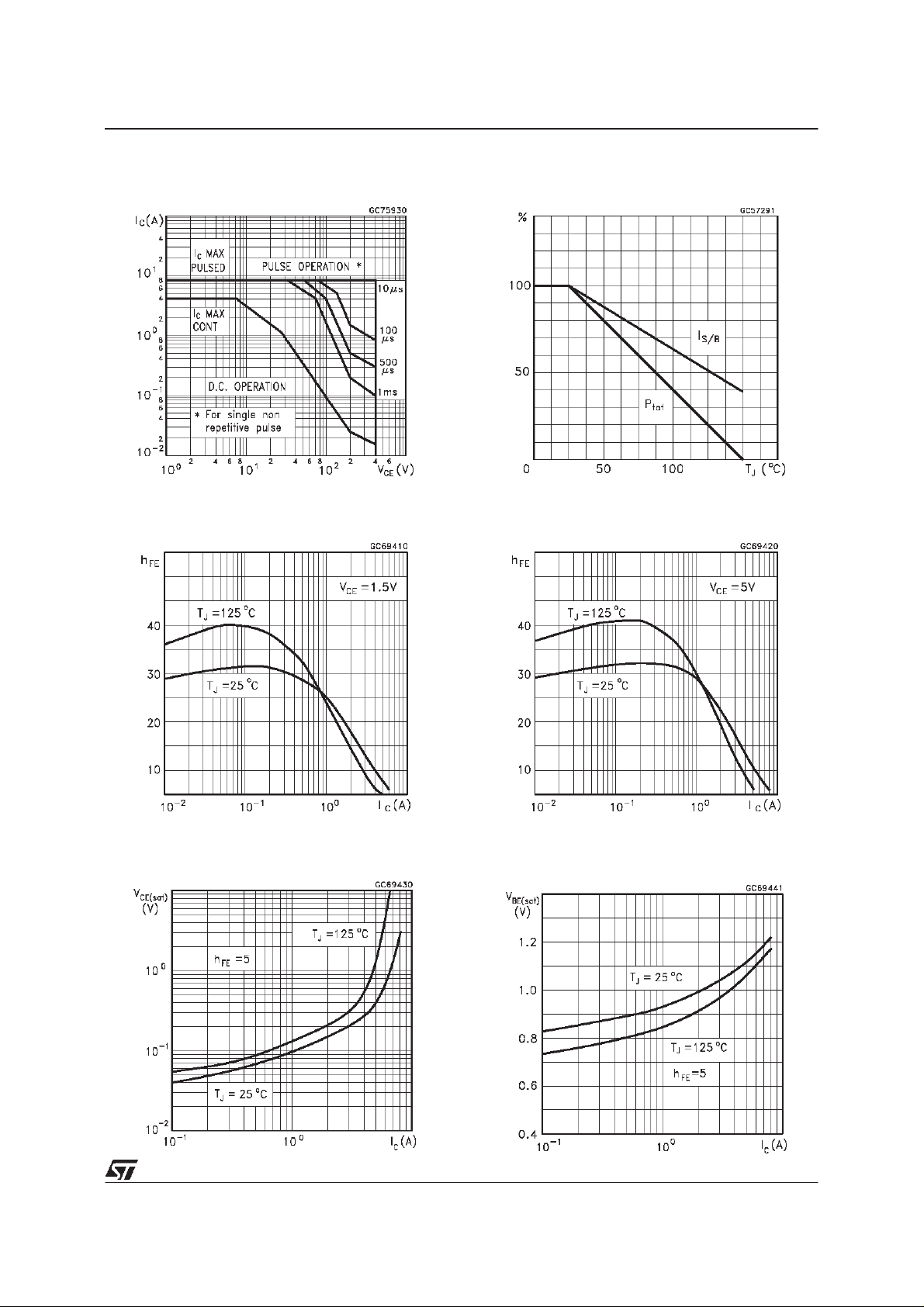
Safe Operating Areas
DCCurrent Gain
DeratingCurve
DC Current Gain
CollectorEmitter SaturationVoltage
BaseEmitter Saturation Voltage
3/7
 Loading...