

HIGH VOLTAGE FAST-SWITCHING
■ STMicroelectronicsPREFERRED
SALESTYPE
■ NPNTRANSISTOR
■ HIGH VOLTAGECAPABILITY
■ LOW SPREADOF DYNAMIC PARAMETERS
■ MINIMUMLOT-TO-LOT SPREAD FOR
RELIABLEOPERATION
■ VERYHIGH SWITCHINGSPEED
■ INTEGRATED ANTIPARALLEL
COLLECTOR-EMITTERDIODE
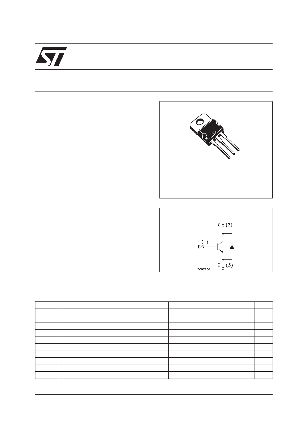
BUL128D-B
NPN POWER TRANSISTOR
3
2
1
APPLICATIONS:
■ ELECTRONICBALLASTSFOR
TO-220
FLUORESCENT LIGHTING
■ FLYBACKAND FORWARDSINGLE
TRANSISTOR LOW POWER CONVERTERS
DESCRIPTION
The device is manufactured using high voltage
INTERNAL SCHEMATIC DIAGRAM
Multi Epitaxial Planar technology for high
switchingspeeds and medium voltage capability.
It uses a Cellular Emitter structure with planar
edge termination to enhance switching speeds
while maintaining the wide RBSOA.
The device is designed for use in lighting
applications and low cost switch-mode power
supplies.
ABSOLUTE MAXIMUM RATINGS
Symbol Parameter Value Unit
V
V
V
I
I
P
T
Collect or-Emit t e r Voltage (VBE= 0) 700 V
CES
Collect or-Emit t e r Voltage (IB= 0) 400 V
CEO
Emitter-Base Voltage (IC=0) 9 V
EBO
Collect or Current 4 A
I
C
Collect or Peak Current (tp<5ms) 8 A
CM
Base Current 2 A
I
B
Base Pea k Curre nt (tp<5ms) 4 A
BM
Tot al Dissipation at Tc=25oC70W
tot
Storage Temperature -65 to 150
stg
Max. Ope r ating Junc tion Tem pe r ature 150
T
j
o
C
o
C
November 1998
1/7
BUL128D-B
THERMAL DATA
R
thj-case
R
thj-amb
Ther mal Resist an c e Junction-Case Max
Ther mal Resist an c e Junction-Ambient Max
1.78
62.5
o
C/W
o
C/W
ELECTRICAL CHARACTERISTICS (T
=25oC unlessotherwise specified)
case
Symbol Parameter Test Cond itions Min. Typ. Max. Unit
I
CES
I
CEO
V
EBO
V
CEO(sus)
Collec t or Cut -off
Current (V
=-1.5V)
BE
Collec t or Cut -off
Current (I
B
=0)
Emitter-Base Voltage IE=10mA 9 V
Collec t or -Emitt er
V
=700V
CE
=700V Tj= 125oC
V
CE
V
= 400 V 250 µA
CE
100
500
IC= 100 m A L = 25 mH 400 V
Sust aining V o lt age
∗ Collector-E mitter
V
CE(sat)
Saturation Voltage
V
∗ Base-Emitt er
BE(sat)
Saturation Voltage
h
∗ DC C ur r ent Gain IC=10mA VCE=5V
FE
V
For ward V o lt age Drop If=2 A 2.5 V
f
INDUCTIV E LOAD
t
s
t
f
Storage Ti me
Fall Time
IC=0.5A IB=0.1A
=1A IB=0.2A
I
C
=2.5A IB=0.5A
I
C
=4A IB=1A 0.5
I
C
IC=0.5A IB=0.1A
=1A IB=0.2A
I
C
=2.5A IB=0.5A
I
C
=2A VCE=5V
I
C
VCC=200 V IC=2A
I
=0.4A V
B1
=0Ω L=200 µH
R
BB
BE(off)
=-5V
10
840
0.6
0.1
0.7
1.0
1.5
1.1
1.2
1.3
(see fig.1)
RESI STIVE LO AD
t
∗
Pulsed: Pulse duration = 300 µs, duty cycle 1.5 %
s
t
f
Storage Ti me
Fall Time
VCC=250V IC=2A
=0.4A IB2=-0.4A
I
B1
=30µs(seefig.2)
T
p
2
0.2
2.9 µs
µA
µA
V
V
V
V
V
V
V
µs
µs
µs
2/7
BUL128D-B
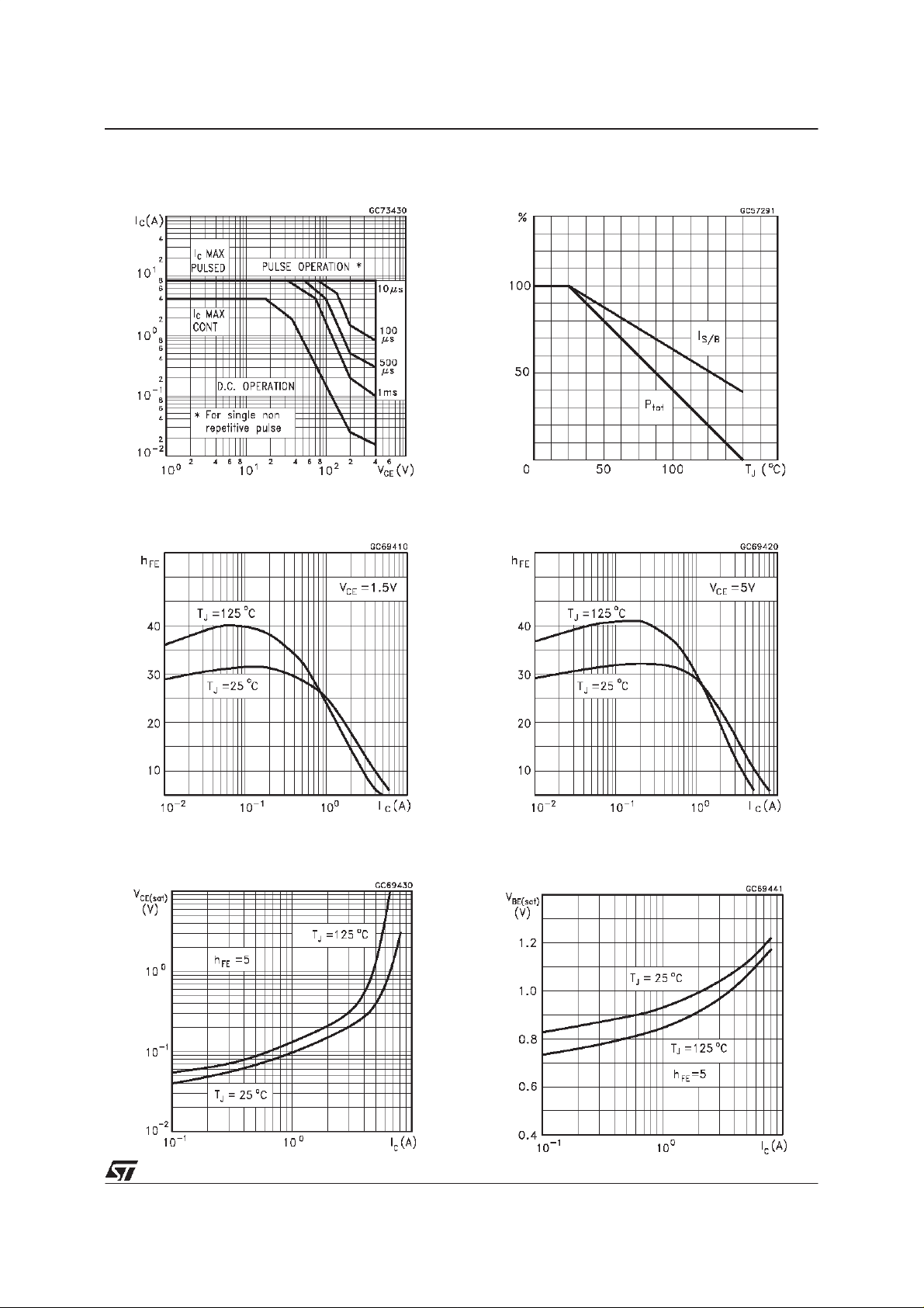
Safe Operating Areas
DCCurrent Gain
DeratingCurve
DC Current Gain
CollectorEmitterSaturationVoltage
BaseEmitterSaturation Voltage
3/7
 Loading...