

SGS Thomson Microelectronics BUL118 Datasheet
HIGH VOLTAGE FAST-SWITCHING
■ NPNTRANSISTOR
■ HIGH VOLTAGECAPABILITY
■ LOW SPREADOF DYNAMIC PARAMETERS
■ MINIMUMLOT-TO-LOT SPREADFOR
RELIABLEOPERATION
■ VERYHIGH SWITCHINGSPEED
APPLICATIONS:
■ ELECTRONICBALLASTSFOR
FLUORESCENT LIGHTING
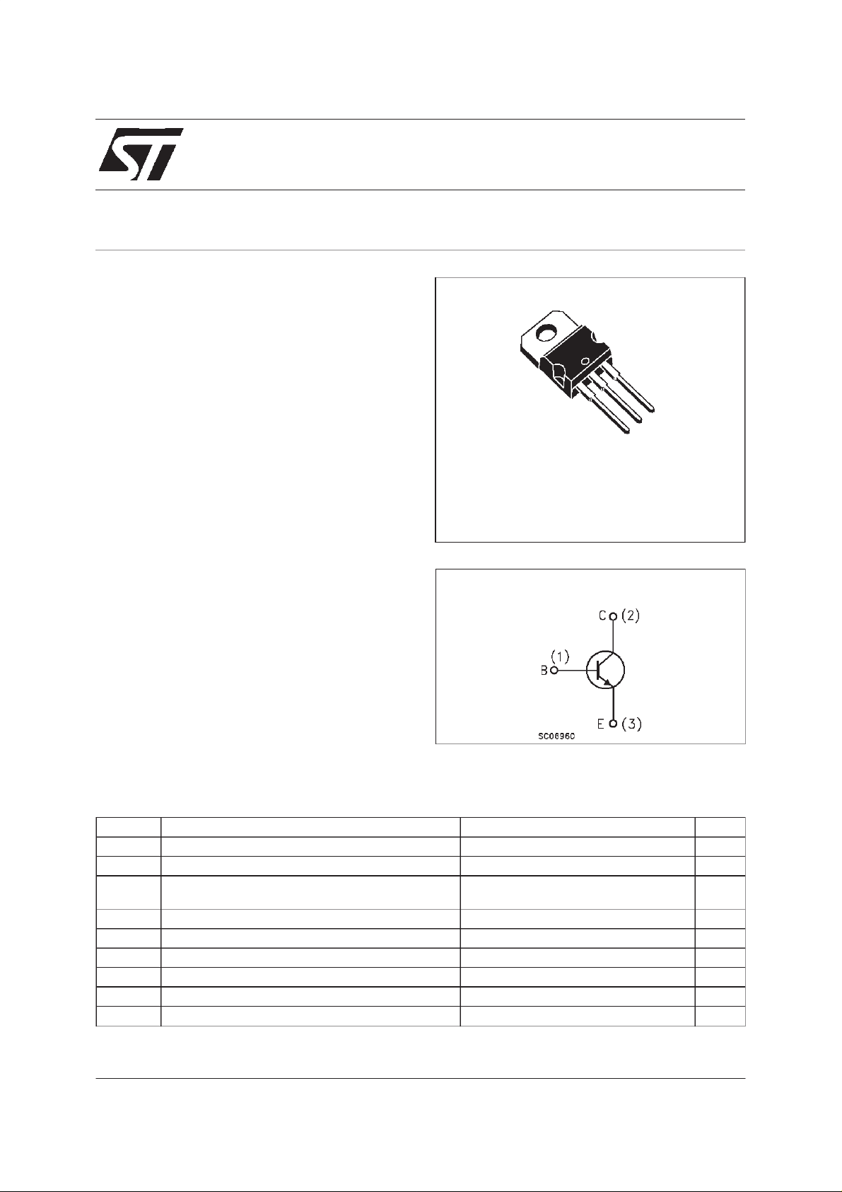
BUL118
NPN POWER TRANSISTOR
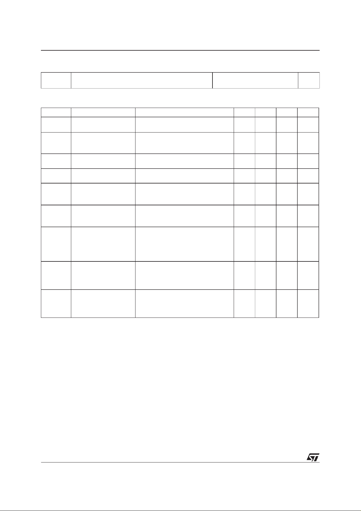
3
2
1
DESCRIPTION
The device is manufactured using high voltage
TO-220
Multi Epitaxial Planar technology for high
switchingspeeds and medium voltage capability.
It uses a Cellular Emitter structure with planar
edge termination to enhance switching speeds
while maintainingthe wide RBSOA.
The device is designed for use in lighting
INTERNAL SCHEMATIC DIAGRAM
applications and low cost switch-mode power
supplies.
ABSOLUTE MAXIMUM RATINGS
Symbol Parameter Value Unit
V
V
V
I
I
P
T
Collect or-Emit t e r Voltage (VBE= 0) 700 V
CES
Collect or-Emit t e r Voltage (IB= 0) 400 V
CEO
Emitter-Base Voltage
EBO
=0,IB<1.5A, tp<10µs , Tj < 150oC)
(I
C
Collect or Current 3 A
I
C
Collect or Peak Current (tp<5ms) 6 A
CM
Base Current 1.5 A
I
B
Base Peak Current (tp<5ms) 3 A
BM
Tot al Di ss ipa t io n at Tc=25oC60W
tot
Storage Temperature -65 to 150
stg
BV
EBO
V
o
C
May 1999
1/7
BUL118
THERMAL DATA
R
thj-case
R
thj-amb
Ther mal Resist an c e Junction-Case Max
Ther mal Resist an c e Junction-Ambient Max
2.08
62.5
o
C/W
o
C/W
ELECTRICAL CHARACTERISTICS (T
=25oC unlessotherwise specified)
case
Symbol Parameter Test Conditions Min. Typ. Max. Un it
BV
I
CES
EBO
Collec t or Cut -off
Current (V
=-1.5V)
BE
Emitt er-Base
V
=700V
CE
=700V Tj= 125oC
V
CE
I
=10mA 9 18 V
E
100
500
µA
µA
Breakdown Voltage
=0)
(I
C
V
CEO(sus)
Collec t or -Emitt er
IC= 100 m A L = 25 mH 400 V
Sust aining Voltage
I
V
CE(sat)
CEO
Collec t or Cut -O ff
Current (I
B
=0)
∗ Collector-E mitter
Saturation Voltage
V
∗ Base-Emitt er
BE(sat)
Saturation Voltage
h
∗ DC Current Ga in IC=10mA VCE=5V
FE
RESI STIVE LOAD
t
Resistive Time
r
t
s
t
f
Storage Time
Fall Time
INDUCTIV E LOAD
t
s
t
f
Storage Time
Fall Time
= 400 V 250 µA
V
CE
IC=0.5A IB=0.1A
=1A IB=0.2A
I
C
=2A IB=0.4A
I
C
IC=0.5A IB=0.1A
=1A IB=0.2A
I
C
=2A IB=0.4A
I
C
0.5
1.3
1.0
1.2
1.3
10
=0.5A VCE=5V
I
C
Gr oup A
Gr oup B
=2A VCE=5V
I
C
10
18
22
40
8
VCC=125 V IC=1A
=0.2A IB2=-0.2A
I
B1
=30µs(seefig.2)
T
p
0.4
3.2
0.25
0.7
4.5
0.4
IC=1A IB1=0.2A
=-5V RBB=0Ω
V
BEo f f
V
= 200 V L = 50mH
clamp
0.8
0.16
V
1
V
V
V
V
V
µs
µs
µs
µs
µs
(see fig.1)
∗
Pulsed: Pulse duration = 300 µs,duty cycle1.5 %
Note : Product is pre-selected inDC current gain (GROUP A and GROUP B).STMicroelectronics reserves the right to ship either groups
according to production availability. Please contact your nearest STMicroelectronics sales office for delivery details.
2/7

BUL118
Safe Operating Areas
DCCurrent Gain
DeratingCurve
DC Current Gain
CollectorEmitterSaturationVoltage
BaseEmitterSaturationVoltage
3/7
 Loading...